Tag: Semiconductors

  • AI Supercharges Semiconductor Spending: Jefferies Upgrades KLA Corporation Amidst Unprecedented Demand

    AI Supercharges Semiconductor Spending: Jefferies Upgrades KLA Corporation Amidst Unprecedented Demand

    In a significant move reflecting the accelerating influence of Artificial Intelligence on the global technology landscape, Jefferies has upgraded KLA Corporation (NASDAQ:KLAC) to a 'Buy' rating, raising its price target to an impressive $1,500 from $1,100. This upgrade, announced on Monday, December 15, 2025, highlights the profound and immediate impact of AI on semiconductor equipment spending, positioning KLA, a leader in process control solutions, at the forefront of this technological revolution. The firm's conviction stems from an anticipated surge in leading-edge semiconductor demand, driven by the insatiable requirements of AI servers and advanced chip manufacturing.

    The re-evaluation of KLA's prospects by Jefferies underscores a broader industry trend where AI is not just a consumer of advanced chips but a powerful catalyst for the entire semiconductor ecosystem. As AI applications demand increasingly sophisticated and powerful processors, the need for cutting-edge manufacturing equipment, particularly in areas like defect inspection and metrology—KLA's specialties—becomes paramount. This development signals a robust multi-year investment cycle in the semiconductor industry, with AI serving as the primary engine for growth and innovation.

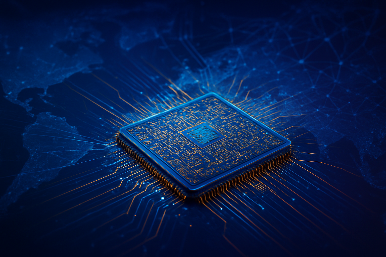
    The Technical Core: AI Revolutionizing Chip Manufacturing and KLA's Role

    AI advancements are profoundly transforming the semiconductor equipment industry, ushering in an era of unprecedented precision, automation, and efficiency in chip manufacturing. KLA Corporation, a leader in process control and yield management solutions, is at the forefront of this transformation, leveraging artificial intelligence across its defect inspection, metrology, and advanced packaging solutions to overcome the escalating complexities of modern chip fabrication.

    The integration of AI into semiconductor equipment significantly enhances several critical aspects of manufacturing. AI-powered systems can process vast datasets from sensors, production logs, and environmental controls in real-time, enabling manufacturers to fine-tune production parameters, minimize waste, and accelerate time-to-market. AI-powered vision systems, leveraging deep learning, achieve defect detection accuracies of up to 99%, analyzing wafer images in real-time to identify imperfections with unmatched precision. This capability extends to recognizing minute irregularities far beyond human vision, reducing the chances of missing subtle flaws. Furthermore, AI algorithms analyze data from various sensors to predict equipment failures before they occur, reducing downtime by up to 30%, and enable real-time feedback loops for process optimization, a stark contrast to traditional, lag-prone inspection methods.

    KLA Corporation aggressively integrates AI into its operations to enhance product offerings, optimize processes, and drive innovation. KLA's process control solutions are indispensable for producing chips that meet the power, performance, and efficiency requirements of AI. For defect inspection, KLA's 8935 inspector employs DefectWise™ AI technology for fast, inline separation of defect types, supporting high-productivity capture of yield and reliability-related defects. For nanoscale precision, the eSL10 e-beam system integrates Artificial Intelligence (AI) with SMARTs™ deep learning algorithms, capable of detecting defects down to 1–3nm. These AI-driven systems significantly outperform traditional human visual inspection or rule-based Automated Optical Inspection (AOI) systems, which struggled with high resolution requirements, inconsistent results, and rigid algorithms unable to adapt to complex, multi-layered structures.

    In metrology, KLA's systems leverage AI to enhance profile modeling, improving measurement accuracy and robustness, particularly for critical overlay measurements in shrinking device geometries. Unlike conventional Optical Critical Dimension (OCD) metrology, which relied on time-consuming physical modeling, AI and machine learning offer much faster solutions by identifying salient spectral features and quantifying their relationships to parameters of interest without extensive physical modeling. For example, Convolutional Neural Networks (CNNs) have achieved 99.9% accuracy in wafer defect pattern recognition, significantly surpassing traditional algorithms. Finally, in advanced packaging—critical for AI chips with 2.5D/3D integration, chiplets, and High Bandwidth Memory (HBM)—KLA's solutions, such as the Kronos™ 1190 wafer-level packaging inspection system and ICOS™ F160XP die sorting and inspection system, utilize AI with deep learning to address new defect types and ensure precise quality control for complex, multi-die heterogeneous integration.

    Market Dynamics: AI's Ripple Effect on Tech Giants and Startups

    The increasing semiconductor equipment spending driven by AI is poised to profoundly impact AI companies, tech giants, and startups from late 2025 to 2027. Global semiconductor sales are projected to reach approximately $1 trillion by 2027, a significant increase driven primarily by surging demand in AI sectors. Semiconductor equipment spending is also expected to grow sustainably, with estimates of $118 billion, $128 billion, and $138 billion for 2025, 2026, and 2027, respectively, reflecting the growing complexity of manufacturing advanced chips. The AI accelerator market alone is projected to grow from $33.69 billion in 2025 to $219.63 billion by 2032, with the market for chips powering generative AI potentially rising to approximately $700 billion by 2027.

    KLA Corporation (NASDAQ:KLAC) is an indispensable leader in process control and yield management solutions, forming the bedrock of the AI revolution. As chip designs become exponentially more complex, KLA's sophisticated inspection and metrology tools are critical for ensuring the precision, quality, and efficiency of next-generation AI chips. KLA's technological leadership is rooted in its comprehensive portfolio covering advanced defect inspection, metrology, and in-situ process monitoring, increasingly augmented by sophisticated AI itself. The company's tools are crucial for manufacturing GPUs with leading-edge nodes, 3D transistor structures, large die sizes, and HBM. KLA has also launched AI-applied wafer-level packaging systems that use deep learning algorithms to enhance defect detection, classification, and improve yield.

    Beyond KLA, leading foundries like TSMC (NYSE:TSM), Samsung Foundry (KRX:005930), and GlobalFoundries (NASDAQ:GFS) are receiving massive investments to expand capacity for AI chip production, including advanced packaging facilities. TSMC, for instance, plans to invest $165 billion in the U.S. for cutting-edge 3nm and 5nm fabs. AI chip designers and producers such as NVIDIA (NASDAQ:NVDA), AMD (NASDAQ:AMD), Intel (NASDAQ:INTC), and Broadcom (NASDAQ:AVGO) are direct beneficiaries. Broadcom, in particular, projects a $60-90 billion revenue opportunity from the AI chip market by fiscal 2027. High-Bandwidth Memory (HBM) manufacturers like SK Hynix (KRX:000660), Samsung, and Micron (NASDAQ:MU) will see skyrocketing demand, with SK Hynix heavily investing in HBM production.

    The increased spending drives a strategic shift towards vertical integration, where tech giants are designing their own custom AI silicon to optimize performance, reduce reliance on third-party suppliers, and achieve cost efficiencies. Google (NASDAQ:GOOGL) with its TPUs, Amazon Web Services (NASDAQ:AMZN) with Trainium and Inferentia chips, Microsoft (NASDAQ:MSFT) with Azure Maia 100, and Meta (NASDAQ:META) with MTIA are prime examples. This strategy allows them to tailor chips to their specific workloads, potentially reducing their dependence on NVIDIA and gaining significant cost advantages. While NVIDIA remains dominant, it faces mounting pressure from these custom ASICs and increasing competition from AMD. Intel is also positioning itself as a "systems foundry for the AI era" with its IDM 2.0 strategy. This shift could disrupt companies heavily reliant on general-purpose hardware without specialized AI optimization, and supply chain vulnerabilities, exacerbated by geopolitical tensions, pose significant challenges for all players.

    Wider Significance: A "Giga Cycle" with Global Implications

    AI's impact on semiconductor equipment spending is intrinsically linked to its broader integration across industries, fueling what many describe as a "giga cycle" of unprecedented scale. This is characterized by a structural increase in long-term market demand for high-performance computing (HPC), requiring specialized neural processing units (NPUs), graphics processing units (GPUs), and high-bandwidth memory (HBM). Beyond data center expansion, the growth of edge AI in devices like autonomous vehicles and industrial robots further necessitates specialized, low-power chips. The global AI in semiconductor market, valued at approximately $56.42 billion in 2024, is projected to reach around $232.85 billion by 2034, with some forecasts suggesting AI accelerators could reach $300-$350 billion by 2029 or 2030, propelling the entire semiconductor market past the trillion-dollar threshold.

    The pervasive integration of AI, underpinned by advanced semiconductors, promises transformative societal impacts across healthcare, automotive, consumer electronics, and infrastructure. AI-optimized semiconductors are essential for real-time processing in diagnostics, genomic sequencing, and personalized treatment plans, while powering the decision-making capabilities of autonomous vehicles. However, this growth introduces significant concerns. AI technologies are remarkably energy-intensive; data centers, crucial for AI workloads, currently consume an estimated 3-4% of the United States' total electricity, with projections indicating a surge to 11-12% by 2030. Semiconductor manufacturing itself is also highly energy-intensive, with a single fabrication plant using as much electricity as a mid-sized city, and TechInsights forecasts a staggering 300% increase in CO2 emissions from AI accelerators alone between 2025 and 2029.

    The global semiconductor supply chain is highly concentrated, with about 75% of manufacturing capacity in China and East Asia, and 100% of the most advanced capacity (below 10 nanometers) located in Taiwan (92%) and South Korea (8%). This concentration creates vulnerabilities to natural disasters, infrastructure disruptions, and geopolitical tensions. The reliance on advanced semiconductor technology for AI has become a focal point of geopolitical competition, particularly between the United States and China, leading to export restrictions and initiatives like the U.S. and E.U. CHIPS Acts to promote domestic manufacturing and diversify supply chains.

    This current AI boom is often described as a "giga cycle," indicating an unprecedented scale of demand that is simultaneously restructuring the economics of compute, memory, networking, and storage. Investment in AI infrastructure is projected to be several times larger than any previous expansion in the industry's history. Unlike some speculative ventures of the dot-com era, today's AI investments are largely financed by highly profitable companies and are already generating substantial value. Previous AI breakthroughs did not necessitate such a profound and specialized shift in hardware infrastructure on this scale, with the demand for highly specialized neural processing units (NPUs) and high-bandwidth memory (HBM) marking a distinct departure from general-purpose computing needs of past eras. Long-term implications include continued investment in R&D for new chip architectures (e.g., 3D chip stacking, silicon photonics), market restructuring, and geopolitical realignments. Ethical considerations surrounding bias, data privacy, and the impact on the global workforce require proactive and thoughtful engagement from industry leaders and policymakers alike.

    The Horizon: Future Developments and Enduring Challenges

    In the near term, AI's insatiable demand for processing power will directly fuel increased semiconductor equipment spending, particularly in advanced logic, high-bandwidth memory (HBM), and sophisticated packaging solutions. The global semiconductor equipment market saw a 21% year-over-year surge in billings in Q1 2025, reaching $32.05 billion, primarily driven by the boom in generative AI and high-performance computing. AI will also be increasingly integrated into semiconductor manufacturing processes to enhance operational efficiencies, including predictive maintenance, automated defect detection, and real-time process control, thereby requiring new, AI-enabled manufacturing equipment.

    Looking further ahead, AI is expected to continue driving sustained revenue growth and significant strategic shifts. The global semiconductor market could exceed $1 trillion in revenue by 2028-2030, with generative AI expansion potentially contributing an additional $300 billion. Long-term trends include the ubiquitous integration of AI into PCs, edge devices, IoT sensors, and autonomous vehicles, driving sustained demand for specialized, low-power, and high-performance chips. Experts predict the emergence of fully autonomous semiconductor fabrication plants where AI not only monitors and optimizes but also independently manages production schedules, resolves issues, and adapts to new designs with minimal human intervention. The development of neuromorphic chips, inspired by the human brain, designed for vastly lower energy consumption for AI tasks, and the integration of AI with quantum computing also represent significant long-term innovations.

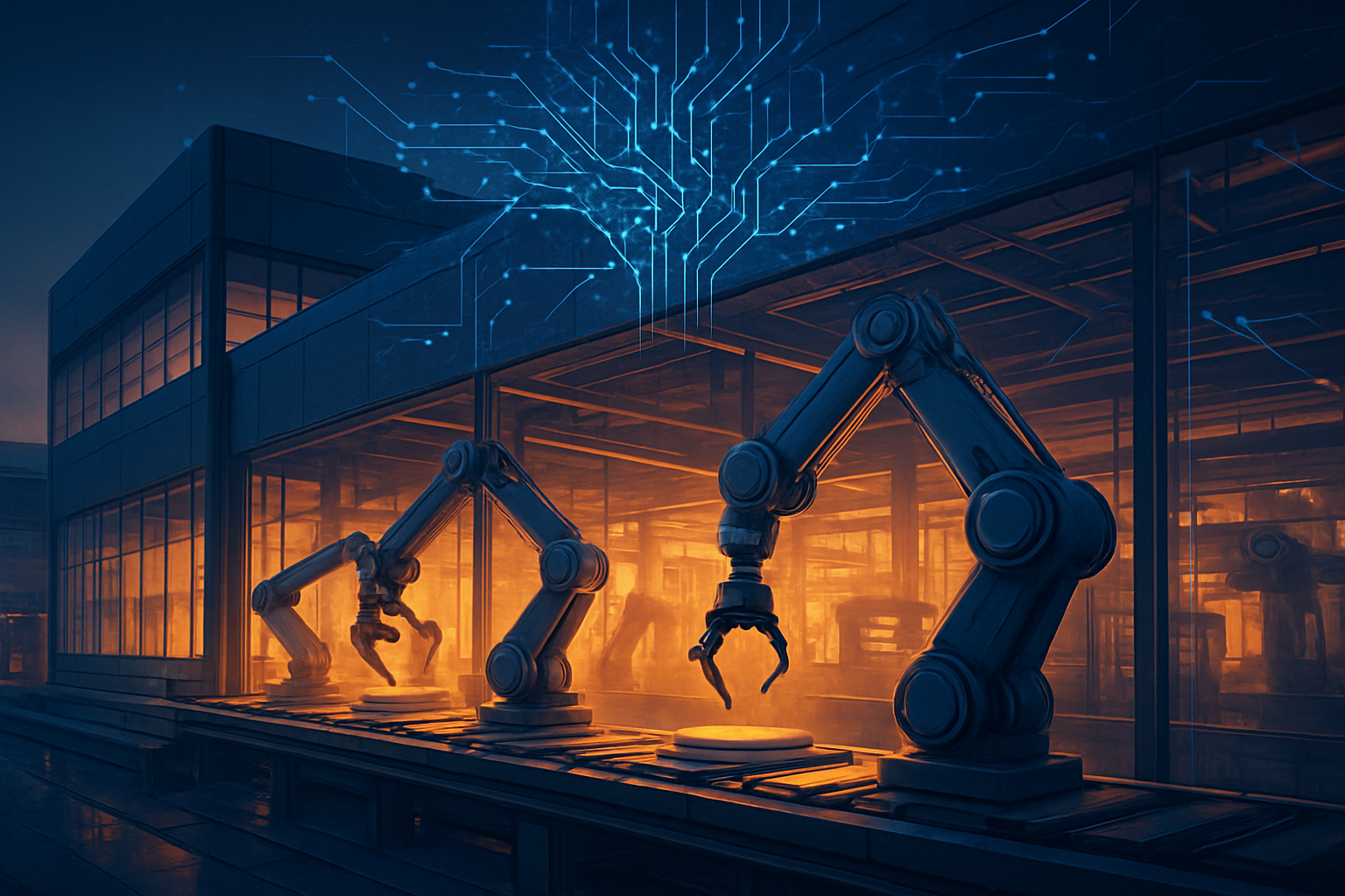
    AI's impact spans the entire semiconductor lifecycle. In chip design, AI-driven Electronic Design Automation (EDA) tools are revolutionizing the process by automating tasks like layout optimization and error detection, drastically reducing design cycles from months to weeks. Tools like Synopsys.ai Copilot and Cadence Cerebrus leverage machine learning to explore billions of design configurations and optimize power, performance, and area (PPA). In manufacturing, AI systems analyze sensor data for predictive maintenance, reducing unplanned downtime by up to 35%, and power computer vision systems for automated defect inspection with unprecedented accuracy. AI also dynamically adjusts manufacturing parameters in real-time for yield enhancement, optimizes energy consumption, and improves supply chain forecasting. For testing and packaging, AI augments validation, improves quality inspection, and helps manage complex manufacturing processes.

    Despite this immense potential, the semiconductor industry faces several enduring challenges. Energy efficiency remains a critical concern, with the significant power demands of advanced lithography, particularly Extreme Ultraviolet (EUV) tools, and the massive electricity consumption of data centers for AI training. Innovations in tool design and AI-driven process optimization are crucial to lower energy requirements. The need for new materials with specific properties for high-performance AI chips and interconnects is a continuous challenge in advanced packaging. Advanced lithography faces hurdles in the cost and complexity of EUV machines and fundamental feature size limits, pushing the industry to explore alternatives like free-electron lasers and direct-write deposition techniques for patterning below 2nm nodes. Other challenges include increasing design complexity at small nodes, rising manufacturing costs (fabs often exceeding $20 billion), a skilled workforce shortage, and persistent supply chain volatility and geopolitical risks. Experts foresee a "giga cycle" driven by specialization and customization, strategic partnerships, an emphasis on sustainability, and the leveraging of generative AI for accelerated innovation.

    Comprehensive Wrap-up: A Defining Era for AI and Semiconductors

    The confluence of Artificial Intelligence and semiconductor manufacturing has ushered in an era of unprecedented investment and innovation, profoundly reshaping the global technology landscape. The Jefferies upgrade of KLA Corporation underscores a critical shift: AI is not merely a technological application but a fundamental force driving a "giga cycle" in semiconductor equipment spending, transforming every facet of chip production from design to packaging. KLA's strategic position as a leader in AI-enhanced process control solutions makes it an indispensable architect of this revolution, enabling the precision and quality required for next-generation AI silicon.

    This period marks a pivotal moment in AI history, signifying a structural realignment towards highly specialized, AI-optimized hardware. Unlike previous technological booms, the current investment is driven by the intrinsic need for advanced computing capabilities to power generative AI, large language models, and autonomous systems. This necessitates a distinct departure from general-purpose computing, fostering innovation in areas like advanced packaging, neuromorphic architectures, and the integration of AI within the manufacturing process itself.

    The long-term impact will be characterized by sustained innovation in chip architectures and fabrication methods, continued restructuring of the industry with an emphasis on vertical integration by tech giants, and ongoing geopolitical realignments as nations vie for technological sovereignty and resilient supply chains. However, this transformative journey is not without its challenges. The escalating energy consumption of AI and chip manufacturing demands a relentless focus on sustainable practices and energy-efficient designs. Supply chain vulnerabilities, exacerbated by geopolitical tensions, necessitate diversified manufacturing footprints. Furthermore, ethical considerations surrounding AI bias, data privacy, and the impact on the global workforce require proactive and thoughtful engagement from industry leaders and policymakers alike.

    As we navigate the coming weeks and months, key indicators to watch will include continued investments in R&D for next-generation lithography and advanced materials, the progress towards fully autonomous fabs, the evolution of AI-specific chip architectures, and the industry's collective response to energy and talent challenges. The "AI chip race" will continue to define competitive dynamics, with companies that can innovate efficiently, secure their supply chains, and address the broader societal implications of AI-driven technology poised to lead this defining era.


    This content is intended for informational purposes only and represents analysis of current AI developments.

    TokenRing AI delivers enterprise-grade solutions for multi-agent AI workflow orchestration, AI-powered development tools, and seamless remote collaboration platforms.
    For more information, visit https://www.tokenring.ai/.

  • UT Austin Unveils QLab: A Quantum Leap for Semiconductor Metrology

    UT Austin Unveils QLab: A Quantum Leap for Semiconductor Metrology

    A groundbreaking development is set to redefine the landscape of semiconductor manufacturing as the University of Texas at Austin announces the establishment of QLab, a state-of-the-art quantum-enhanced semiconductor metrology facility. Unveiled on December 10, 2025, this cutting-edge initiative, backed by a significant $4.8 million grant from the Texas Semiconductor Innovation Fund (TSIF), is poised to integrate advanced quantum science into the highly precise measurement processes critical for producing next-generation microchips.

    QLab's immediate significance is profound. By pushing the boundaries of metrology – the science of measurement at atomic and molecular scales – the facility will tackle some of the most pressing challenges in semiconductor fabrication. This strategic investment not only solidifies Texas's position as a leader in semiconductor innovation but also aims to cultivate a robust ecosystem for both the burgeoning quantum industry and the established semiconductor sector, promising to generate thousands of high-paying jobs and foster critical academic research.

    Quantum Precision: Diving Deep into QLab's Technical Edge

    QLab is poised to become a nexus for innovation, specifically designed to address the escalating measurement challenges in advanced semiconductor manufacturing. Under the stewardship of the Texas Quantum Institute (TQI) in collaboration with UT Austin's Microelectronics Research Center (MRC), Texas Institute for Electronics (TIE), and Texas Materials Institute (TMI), the facility will acquire and deploy state-of-the-art instrumentation. This sophisticated equipment will harness the latest advancements in quantum science and technology to develop precise tools for the fabrication and meticulous analysis of materials and devices at the atomic scale. The strategic integration of these research powerhouses ensures a holistic approach to advancing both fundamental and applied research in quantum-enhanced metrology.

    The distinction between traditional and quantum-enhanced metrology is stark and crucial for the future of chip production. Conventional metrology, while effective for larger geometries, faces significant limitations as semiconductor features shrink below 5 nanometers and move into complex 3D architectures like FinFETs. Issues such as insufficient 2D measurements for 3D structures, difficulties in achieving precision for sub-5 nm stochastic processes, and physical property changes at quantum confinement scales hinder progress. Furthermore, traditional optical metrology struggles with obstruction by metal layers in the back-end-of-line manufacturing, and high-resolution electron microscopy, while powerful, can be too slow for high-throughput, non-destructive, and inline production demands.

    Quantum-enhanced metrology, by contrast, leverages fundamental quantum phenomena such as superposition and entanglement to achieve unparalleled levels of precision and sensitivity. This approach inherently offers significant noise reduction, leading to far more accurate results at atomic and subatomic scales. Quantum sensors, for example, can detect minute defects in intricate 3D and heterogeneous architectures and perform measurements even through metal layers where optical methods fail. Diamond-based quantum sensors exemplify this capability, enabling non-destructive, 3D mapping of magnetic fields on wafers to pinpoint defects. The integration of computational modeling and machine learning further refines defect identification and current flow mapping, potentially achieving nanometer-range resolutions. Beyond manufacturing, these quantum measurement techniques also promise advancements in quantum communications and computing.

    Initial reactions from the broader scientific and industrial communities have been overwhelmingly positive, reflecting a clear understanding of metrology's critical role in the semiconductor ecosystem. While specific "initial reactions" from individual AI researchers were not explicitly detailed, the robust institutional and governmental support speaks volumes. Governor Greg Abbott and Senator Sarah Eckhardt have lauded QLab, emphasizing its potential to cement Texas's leadership in both the semiconductor and emerging quantum industries and generate high-paying jobs. Elaine Li, Co-director of the Texas Quantum Institute, expressed gratitude for the state's investment, acknowledging the "tremendous momentum" it brings. Given UT Austin's significant investment in AI research—including nearly half a billion dollars in new AI projects in 2024 and one of academia's largest AI computing clusters—it is clear that QLab will operate within a highly synergistic environment where advanced quantum metrology can both benefit from and contribute to cutting-edge AI capabilities in data analysis, computational modeling, and process optimization.

    Catalytic Impact: Reshaping the AI and Semiconductor Industries

    The establishment of QLab at UT Austin carries significant implications for a broad spectrum of companies, particularly within the semiconductor and AI sectors. While direct beneficiaries will primarily be Texas-based semiconductor companies and global semiconductor manufacturers like Intel (NASDAQ: INTC), Taiwan Semiconductor Manufacturing Company (NYSE: TSM), and Samsung (KRX: 005930), which are constantly striving for higher precision and yields in chip fabrication, the ripple effects will extend far and wide. Companies specializing in quantum technology, such as IBM (NYSE: IBM) and Google (NASDAQ: GOOGL) with their quantum computing initiatives, will also find QLab a valuable resource for overcoming manufacturing hurdles in building stable and scalable quantum hardware.

    For major AI labs and tech giants, QLab's advancements in semiconductor metrology offer a crucial, albeit indirect, competitive edge. More powerful, efficient, and specialized chips, enabled by quantum-enhanced measurements, are the bedrock for accelerating AI computation, training colossal large language models, and deploying AI at the edge. This means companies like NVIDIA (NASDAQ: NVDA), a leading designer of AI accelerators, and cloud providers like Amazon (NASDAQ: AMZN) Web Services, Microsoft (NASDAQ: MSFT) Azure, and Google Cloud, which heavily rely on advanced hardware for their AI services, stand to benefit from the enhanced performance and reduced costs that improved chip manufacturing can deliver. The ability to integrate QLab's breakthroughs into their hardware design and manufacturing processes will confer a strategic advantage, allowing them to push the boundaries of AI capabilities.

    While QLab is unlikely to directly disrupt existing consumer products or services immediately, its work on advancing the manufacturing process of semiconductors will act as a powerful enabler for future disruption. By making possible the creation of more complex, efficient, or entirely novel types of semiconductors, QLab will enable breakthroughs across various industries. Imagine vastly improved chips leading to unprecedented advancements in autonomous systems, advanced sensors, and quantum devices that are currently constrained by hardware limitations. Furthermore, enhanced metrology can lead to higher manufacturing yields and reduced defects, potentially lowering the cost of producing advanced semiconductors. This could indirectly disrupt markets by making cutting-edge technologies more accessible or by boosting profit margins for chipmakers. QLab's research could also set new industry standards and tools for semiconductor testing and quality control, potentially rendering older, less precise methods obsolete over time.

    Strategically, QLab significantly elevates the market positioning of both Texas and the University of Texas at Austin as global leaders in semiconductor innovation and quantum research. This magnetism will attract top talent and investment, reinforcing the region's role in a critical global industry. For companies that partner with or leverage QLab's expertise, access to cutting-edge quantum science for semiconductor manufacturing provides a distinct strategic advantage in developing next-generation chips with superior performance, reliability, and efficiency. As semiconductors continue their relentless march towards miniaturization and complexity, QLab's quantum-enhanced metrology offers a critical advantage in pushing these boundaries. By fostering an ecosystem of innovation that bridges academic research with industrial needs, QLab accelerates the translation of quantum science discoveries into practical applications for semiconductor manufacturing and, by extension, the entire AI landscape, while also strengthening domestic supply chain resilience.

    Wider Significance: A New Era for AI and Beyond

    The QLab facility at UT Austin is not merely an incremental upgrade; it represents a foundational shift that will profoundly impact the broader AI landscape and technological trends. By focusing on quantum-enhanced semiconductor metrology, QLab directly addresses the most critical bottleneck in the relentless pursuit of more powerful and energy-efficient AI hardware: the precision of chip manufacturing at the atomic scale. As AI models grow exponentially in complexity and demand, the ability to produce flawless, ultra-dense semiconductors becomes paramount. QLab's work underpins the viability of next-generation AI processors, from specialized accelerators like Google's (NASDAQ: GOOGL) Tensor Processing Units (TPUs) to advanced Graphics Processing Units (GPUs) from NVIDIA (NASDAQ: NVDA) and emerging photonic processors. It also aligns with the growing trend of integrating AI and machine learning into industrial metrology itself, transforming discrete measurements into a continuous digital feedback loop across design, manufacturing, and inspection.

    The societal and technological impacts of QLab are far-reaching. Technologically, it will significantly advance semiconductor manufacturing in Texas, solidifying the state's position as a national innovation hub and facilitating the production of more sophisticated and reliable chips essential for everything from smartphones and cloud servers to autonomous vehicles and advanced robotics. By fostering breakthroughs in both the semiconductor and nascent quantum industries, QLab is expected to accelerate research and development cycles and reduce manufacturing costs, pushing engineering capabilities beyond what classical high-performance computing can achieve today. Societally, the facility is projected to fuel regional economic growth through the creation of high-paying advanced manufacturing jobs, strengthen academic research, and support workforce development, nurturing a skilled talent pipeline for these critical sectors. Furthermore, by contributing to domestic semiconductor manufacturing, QLab indirectly enhances national technological independence and supply chain resilience for vital electronic components.

    However, QLab's unique capabilities also bring potential concerns, primarily related to the nascent nature of quantum technologies and the complexities of AI integration. Quantum computing, while promising, is still an immature technology, facing challenges with noise, error rates, and qubit stability. The seamless integration of classical and quantum systems presents a formidable engineering hurdle. Moreover, the effectiveness of AI in semiconductor metrology can be limited by data veracity, insufficient datasets for training AI models, and ensuring cross-scale compatibility of measurement data. While not a direct concern for QLab specifically, the broader ethical implications of advanced AI and quantum technology, such as potential job displacement due to automation in manufacturing and the dual-use nature of cutting-edge chip technology, remain important considerations for responsible development and access.

    Comparing QLab's establishment to previous AI hardware milestones reveals its distinct foundational significance. Historically, AI hardware evolution progressed from general-purpose CPUs to the massive parallelism of GPUs, then to purpose-built ASICs like Google's TPUs. These milestones focused on enhancing computational architecture. QLab, however, focuses on the foundational manufacturing and quality control of the semiconductors themselves, using quantum metrology to perfect the very building blocks at an unprecedented atomic scale. This addresses a critical bottleneck: as chips become smaller and more complex, the ability to accurately measure, inspect, and verify their properties becomes paramount for continued progress. Therefore, QLab represents a pivotal enabler for all future AI hardware generations, ensuring that physical manufacturing limitations do not impede the ongoing "quantum leaps" in AI innovation. It is a foundational milestone that underpins the viability of all subsequent computational hardware advancements.

    The Horizon of Innovation: Future Developments and Applications

    The establishment of QLab at UT Austin signals a future where the physical limits of semiconductor technology are continually pushed back through the lens of quantum science. In the near term, QLab's primary focus will be on the rapid development and refinement of ultra-precise measurement tools. This includes the acquisition and deployment of cutting-edge instrumentation specifically designed to leverage quantum phenomena for metrology at atomic and molecular scales. The immediate goal is to address the most pressing measurement challenges currently facing next-generation chip manufacturing, ensuring higher yields, greater reliability, and the continued miniaturization of components.

    Looking further ahead, QLab is positioned to become a cornerstone in the evolution of both the semiconductor and emerging quantum industries. Its long-term vision extends to driving fundamental breakthroughs that will shape the very fabric of future technology. Potential applications and use cases are vast and transformative. Beyond enabling the fabrication of more powerful and efficient microchips for AI, cloud computing, and advanced electronics, QLab will directly support the development of quantum technologies themselves, including quantum computing, quantum sensing, and quantum communication. It will also serve as a vital hub for academic research, fostering interdisciplinary collaboration and nurturing a skilled workforce ready for the demands of advanced manufacturing and quantum science. This includes not just engineers and physicists, but also data scientists who can leverage AI to analyze the unprecedented amounts of precision data generated by quantum metrology.

    The central challenge QLab is designed to address is the escalating demand for precision in semiconductor manufacturing. As feature sizes shrink to the sub-nanometer realm, conventional measurement methods simply cannot provide the necessary accuracy. QLab seeks to overcome these "critical challenges" by employing quantum-enhanced metrology, enabling the industry to continue its trajectory of innovation. Another implicit challenge is to ensure that Texas maintains and strengthens its leadership in the highly competitive global semiconductor and quantum technology landscape, a goal explicitly supported by the Texas CHIPS Act and the strategic establishment of QLab.

    Experts are resoundingly optimistic about QLab's prospects. Governor Greg Abbott has declared, "Texas is the new frontier of innovation and UT Austin is where world-changing discoveries in quantum research and development are being made," predicting that QLab will help Texas "continue to lead the nation with quantum leaps into the future." Elaine Li, Co-director of the Texas Quantum Institute, underscored metrology's role as a "key enabling technology for the semiconductor industry" and anticipates that QLab's investment will empower UT Austin to advance metrology tools to solve critical sector challenges. Co-director Xiuling Li added that this investment provides "tremendous momentum to advance quantum-enhanced semiconductor metrology, driving breakthroughs that will shape the future of both the semiconductor and quantum industries." These predictions collectively paint a picture of QLab as a pivotal institution that will not only solve present manufacturing hurdles but also unlock entirely new possibilities for the future of technology and AI.

    A Quantum Leap for the Digital Age: The Future is Measured

    The establishment of QLab at the University of Texas at Austin marks a watershed moment in the intertwined histories of semiconductor manufacturing and artificial intelligence. Backed by a $4.8 million grant from the Texas Semiconductor Innovation Fund and announced on December 10, 2025, this quantum-enhanced metrology facility is poised to revolutionize how we build the very foundation of our digital world. Its core mission—to apply advanced quantum science to achieve unprecedented precision in chip measurement—is not just an incremental improvement; it is a foundational shift that will enable the continued miniaturization and increased complexity of the microchips that power every AI system, from the smallest edge devices to the largest cloud supercomputers.

    The significance of QLab cannot be overstated. It directly addresses the looming physical limits of traditional semiconductor manufacturing, offering a quantum solution to a classical problem. By ensuring atomic-scale precision in chip fabrication, QLab will unlock new frontiers for AI hardware, leading to more powerful, efficient, and reliable processors. This, in turn, will accelerate AI research, enable more sophisticated AI applications, and solidify the competitive advantages of companies that can leverage these advanced capabilities. Beyond the immediate technological gains, QLab is a strategic investment in economic growth, job creation, and national technological sovereignty, positioning Texas and the U.S. at the forefront of the next wave of technological innovation.

    As we look ahead, the impact of QLab will unfold in fascinating ways. We can expect near-term advancements in chip yield and performance, followed by long-term breakthroughs in quantum computing and sensing, all underpinned by QLab's metrology prowess. While challenges remain in integrating nascent quantum technologies and managing vast datasets with AI, the collective optimism of experts suggests that QLab is well-equipped to navigate these hurdles. This facility is more than just a lab; it is a testament to the power of interdisciplinary research and strategic investment, promising to shape not just the future of semiconductors, but the entire digital age.

    What to watch for in the coming weeks and months will be the initial instrument procurements, key research partnerships with industry, and early academic publications stemming from QLab's work. These initial outputs will provide the first tangible insights into the "quantum leaps" that UT Austin, with its new QLab, is prepared to deliver.


    This content is intended for informational purposes only and represents analysis of current AI developments.

    TokenRing AI delivers enterprise-grade solutions for multi-agent AI workflow orchestration, AI-powered development tools, and seamless remote collaboration platforms.
    For more information, visit https://www.tokenring.ai/.

  • The Dawn of a New Era: Semiconductor Innovations Propel AI, HPC, and Mobile into Uncharted Territory

    The Dawn of a New Era: Semiconductor Innovations Propel AI, HPC, and Mobile into Uncharted Territory

    As of late 2025, the semiconductor industry stands at the precipice of a profound transformation, driven by an insatiable demand for computational power across Artificial Intelligence (AI), High-Performance Computing (HPC), and the rapidly evolving mobile sector. This period marks a pivotal shift beyond the conventional limits of Moore's Law, as groundbreaking advancements in chip design and novel architectures are fundamentally redefining how technology delivers intelligence and performance. These innovations are not merely incremental improvements but represent a systemic re-architecture of computing, promising to unlock unprecedented capabilities and reshape the technological landscape for decades to come.

    The immediate significance of these developments cannot be overstated. From enabling the real-time processing of colossal AI models to facilitating complex scientific simulations and powering smarter, more efficient mobile devices, the next generation of semiconductors is the bedrock upon which future technological breakthroughs will be built. This foundational shift is poised to accelerate innovation across industries, fostering an era of more intelligent systems, faster data analysis, and seamlessly integrated digital experiences.

    Technical Revolution: Unpacking the Next-Gen Semiconductor Landscape

    The core of this revolution lies in several intertwined technical advancements that are collectively pushing the boundaries of what's possible in silicon.

    The most prominent shift is towards Advanced Packaging and Heterogeneous Integration, particularly through chiplet technology. Moving away from monolithic System-on-Chip (SoC) designs, manufacturers are now integrating multiple specialized "chiplets"—each optimized for a specific function like logic, memory, or I/O—into a single package. This modular approach offers significant advantages: vastly increased performance density, improved energy efficiency through closer proximity and advanced interconnects, and highly customizable architectures tailored for specific AI, HPC, or embedded applications. Technologies like 2.5D and 3D stacking, including chip-on-wafer-on-substrate (CoWoS) and through-silicon vias (TSVs), are critical enablers, providing ultra-short, high-density connections that drastically reduce latency and power consumption. Early prototypes of monolithic 3D integration, where layers are built sequentially on the same wafer, are also demonstrating substantial gains in both performance and energy efficiency.

    Concurrently, the relentless pursuit of smaller process nodes continues, albeit with increasing complexity. By late 2025, the industry is seeing the widespread adoption of 3-nanometer (nm) and 2nm manufacturing processes. Leading foundries like TSMC (NYSE: TSM) are on track with their A16 (1.6nm) nodes for production in 2026, while Intel (NASDAQ: INTC) is pushing towards its 1.8nm (Intel 18A) node. These finer geometries allow for higher transistor density, translating directly into superior performance and greater power efficiency, crucial for demanding AI and HPC workloads. Furthermore, the integration of advanced materials is playing a pivotal role. Silicon Carbide (SiC) and Gallium Nitride (GaN) are becoming standard for power components, offering higher breakdown voltages, faster switching speeds, and greater power density, which is particularly vital for the energy-intensive data centers powering AI and HPC. Research into novel 3D DRAM using oxide-semiconductors and carbon nanotube transistors also promises high-density, low-power memory solutions.

    Perhaps one of the most intriguing developments is the increasing role of AI in chip design and manufacturing itself. AI-powered Electronic Design Automation (EDA) tools are automating complex tasks like schematic generation, layout optimization, and verification, drastically shortening design cycles—what once took months for a 5nm chip can now be achieved in weeks. AI also enhances manufacturing efficiency through predictive maintenance, real-time process optimization, and sophisticated defect detection, ensuring higher yields and faster time-to-market for these advanced chips. This self-improving loop, where AI designs better chips for AI, represents a significant departure from traditional, human-intensive design methodologies. The initial reactions from the AI research community and industry experts are overwhelmingly positive, with many hailing these advancements as the most significant architectural shifts since the rise of the GPU, setting the stage for an exponential leap in computational capabilities.

    Industry Shake-Up: Winners, Losers, and Strategic Plays

    The seismic shifts in semiconductor technology are poised to create significant ripples across the tech industry, reordering competitive landscapes and establishing new strategic advantages. Several key players stand to benefit immensely, while others may face considerable disruption if they fail to adapt.

    NVIDIA (NASDAQ: NVDA), a dominant force in AI and HPC GPUs, is exceptionally well-positioned. Their continued innovation in GPU architectures, coupled with aggressive adoption of HBM and CXL technologies, ensures they remain at the forefront of AI training and inference. The shift towards heterogeneous integration and specialized accelerators complements NVIDIA's strategy of offering a full-stack solution, from hardware to software. Similarly, Intel (NASDAQ: INTC) and Advanced Micro Devices (NASDAQ: AMD) are making aggressive moves to capture market share. Intel's focus on advanced process nodes (like Intel 18A) and its strong play in CXL and CPU-GPU integration positions it as a formidable competitor, especially in data center and HPC segments. AMD, with its robust CPU and GPU offerings and increasing emphasis on chiplet designs, is also a major beneficiary, particularly in high-performance computing and enterprise AI.

    The foundries, most notably Taiwan Semiconductor Manufacturing Company (TSMC) (NYSE: TSM) and Samsung Electronics (KRX: 005930), are critical enablers and direct beneficiaries. Their ability to deliver cutting-edge process nodes (3nm, 2nm, and beyond) and advanced packaging solutions (CoWoS, 3D stacking) makes them indispensable to the entire tech ecosystem. Companies that can secure capacity at these leading-edge foundries will gain a significant competitive edge. Furthermore, major cloud providers like Amazon (NASDAQ: AMZN) (AWS), Google (NASDAQ: GOOGL) (Google Cloud), and Microsoft (NASDAQ: MSFT) (Azure) are heavily investing in custom Application-Specific Integrated Circuits (ASICs) for their AI workloads. The chiplet approach and advanced packaging allow these tech giants to design highly optimized, cost-effective, and energy-efficient AI accelerators tailored precisely to their internal software stacks, potentially disrupting traditional GPU markets for specific AI tasks. This strategic move provides them greater control over their infrastructure, reduces reliance on third-party hardware, and can offer 10-100x efficiency improvements for specific AI operations compared to general-purpose GPUs.

    Startups specializing in novel AI architectures, particularly those focused on neuromorphic computing or highly efficient edge AI processors, also stand to gain. The modularity of chiplets lowers the barrier to entry for designing specialized silicon, allowing smaller companies to innovate without the prohibitive costs of designing entire monolithic SoCs. However, established players with deep pockets and existing ecosystem advantages will likely consolidate many of these innovations. The competitive implications are clear: companies that can rapidly adopt and integrate these new chip design paradigms will thrive, while those clinging to older, less efficient architectures risk being left behind. The market is increasingly valuing power efficiency, customization, and integrated performance, forcing every major player to rethink their silicon strategy.

    Wider Significance: Reshaping the AI and Tech Landscape

    These anticipated advancements in semiconductor chip design and architecture are far more than mere technical upgrades; they represent a fundamental reshaping of the broader AI landscape and global technological trends. This era marks a critical inflection point, moving beyond the incremental gains of the past to a period of transformative change.

    Firstly, these developments significantly accelerate the trajectory of Artificial General Intelligence (AGI) research and deployment. The massive increase in computational power, memory bandwidth, and energy efficiency provided by chiplets, HBM, CXL, and specialized accelerators directly addresses the bottlenecks that have hindered the training and inference of increasingly complex AI models, particularly large language models (LLMs). This enables researchers to experiment with larger, more intricate neural networks and develop AI systems capable of more sophisticated reasoning and problem-solving. The ability to run these advanced AIs closer to the data source, on edge devices, also expands the practical applications of AI into real-time scenarios where latency is critical.

    The impact on data centers is profound. CXL, in particular, allows for memory disaggregation and pooling, turning memory into a composable resource that can be dynamically allocated across CPUs, GPUs, and accelerators. This eliminates costly over-provisioning, drastically improves utilization, and reduces the total cost of ownership for AI and HPC infrastructure. The enhanced power efficiency from smaller process nodes and advanced materials also helps mitigate the soaring energy consumption of modern data centers, addressing both economic and environmental concerns. However, potential concerns include the increasing complexity of designing and manufacturing these highly integrated systems, leading to higher development costs and the potential for a widening gap between companies that can afford to innovate at the cutting edge and those that cannot. This could exacerbate the concentration of AI power in the hands of a few tech giants.

    Comparing these advancements to previous AI milestones, this period is arguably as significant as the advent of GPUs for parallel processing or the breakthroughs in deep learning algorithms. While past milestones focused on software or specific hardware components, the current wave involves a holistic re-architecture of the entire computing stack, from the fundamental silicon to system-level integration. The move towards specialized, heterogeneous computing is reminiscent of how the internet evolved from general-purpose servers to a highly distributed, specialized network. This signifies a departure from a one-size-fits-all approach to computing, embracing diversity and optimization for specific workloads. The implications extend beyond technology, touching on national security (semiconductor independence), economic competitiveness, and the ethical considerations of increasingly powerful AI systems.

    The Road Ahead: Future Developments and Challenges

    Looking to the horizon, the advancements in semiconductor technology promise an exciting array of near-term and long-term developments, while also presenting significant challenges that the industry must address.

    In the near term, we can expect the continued refinement and widespread adoption of chiplet architectures and 3D stacking technologies. This will lead to increasingly dense and powerful processors for cloud AI and HPC, with more sophisticated inter-chiplet communication. The CXL ecosystem will mature rapidly, with CXL 3.0 and beyond enabling even more robust multi-host sharing and switching capabilities, truly unlocking composable memory and compute infrastructure in data centers. We will also see a proliferation of highly specialized edge AI accelerators integrated into a wider range of devices, from smart home appliances to industrial IoT sensors, making AI ubiquitous and context-aware. Experts predict that the performance-per-watt metric will become the primary battleground, as energy efficiency becomes paramount for both environmental sustainability and economic viability.

    Longer term, the industry is eyeing monolithic 3D integration as a potential game-changer, where entire functional layers are built directly on top of each other at the atomic level, promising unprecedented performance and energy efficiency. Research into neuromorphic chips designed to mimic the human brain's neural networks will continue to advance, potentially leading to ultra-low-power AI systems capable of learning and adapting with significantly reduced energy footprints. Quantum computing, while still nascent, will also increasingly leverage advanced packaging and cryogenic semiconductor technologies. Potential applications on the horizon include truly personalized AI assistants that learn and adapt deeply to individual users, autonomous systems with real-time decision-making capabilities far beyond current capacities, and breakthroughs in scientific discovery driven by exascale HPC systems.

    However, significant challenges remain. The cost and complexity of manufacturing at sub-2nm nodes are escalating, requiring immense capital investment and sophisticated engineering. Thermal management in densely packed 3D architectures becomes a critical hurdle, demanding innovative cooling solutions. Supply chain resilience is another major concern, as geopolitical tensions and the highly concentrated nature of advanced manufacturing pose risks. Furthermore, the industry faces a growing talent gap in chip design, advanced materials science, and packaging engineering. Experts predict that collaboration across the entire semiconductor ecosystem—from materials suppliers to EDA tool vendors, foundries, and system integrators—will be crucial to overcome these challenges and fully realize the potential of these next-generation semiconductors. What happens next will largely depend on sustained investment in R&D, international cooperation, and a concerted effort to nurture the next generation of silicon innovators.

    Comprehensive Wrap-Up: A New Era of Intelligence

    The anticipated advancements in semiconductor chip design, new architectures, and their profound implications mark a pivotal moment in technological history. The key takeaways are clear: the industry is moving beyond traditional scaling with heterogeneous integration and chiplets as the new paradigm, enabling unprecedented customization and performance density. Memory-centric architectures like HBM and CXL are revolutionizing data access and system efficiency, while specialized AI accelerators are driving bespoke intelligence across all sectors. Finally, AI itself is becoming an indispensable tool in the design and manufacturing of these sophisticated chips, creating a powerful feedback loop.

    This development's significance in AI history is monumental. It provides the foundational hardware necessary to unlock the next generation of AI capabilities, from more powerful large language models to ubiquitous edge intelligence and scientific breakthroughs. It represents a shift from general-purpose computing to highly optimized, application-specific silicon, mirroring the increasing specialization seen in other mature industries. This is not merely an evolution but a revolution in how we design and utilize computing power.

    Looking ahead, the long-term impact will be a world where AI is more pervasive, more powerful, and more energy-efficient than ever before. We can expect a continued acceleration of innovation in autonomous systems, personalized medicine, advanced materials science, and climate modeling. What to watch for in the coming weeks and months includes further announcements from leading chip manufacturers regarding their next-generation process nodes and packaging technologies, the expansion of the CXL ecosystem, and the emergence of new AI-specific hardware from both established tech giants and innovative startups. The race to build the most efficient and powerful silicon is far from over; in fact, it's just getting started.


    This content is intended for informational purposes only and represents analysis of current AI developments.

    TokenRing AI delivers enterprise-grade solutions for multi-agent AI workflow orchestration, AI-powered development tools, and seamless remote collaboration platforms.
    For more information, visit https://www.tokenring.ai/.

  • The Great Silicon Divide: Geopolitical Tensions Forge New Frontiers in Chip Development and Alliances

    The Great Silicon Divide: Geopolitical Tensions Forge New Frontiers in Chip Development and Alliances

    The global semiconductor industry, a foundational pillar of modern technology, is undergoing an unprecedented transformation driven by escalating geopolitical tensions, often dubbed the "Tech War." As of late 2025, the rivalry, predominantly between the United States and China, has elevated semiconductors from mere components to strategic national assets, fundamentally reshaping indigenous chip development efforts and fostering new strategic alliances worldwide. This paradigm shift marks a departure from a globally integrated, efficiency-driven supply chain towards a more fragmented, resilience-focused landscape, with profound implications for technological innovation and global power dynamics.

    The immediate significance of these tensions is the accelerating push for technological sovereignty, as nations pour massive investments into developing their own domestic chip capabilities to mitigate reliance on foreign supply chains. This strategic pivot is leading to the emergence of distinct regional ecosystems, potentially ushering in an era of "two competing digital worlds." The repercussions are far-reaching, impacting everything from the cost of electronic devices to the future trajectory of advanced technologies like Artificial Intelligence (AI) and quantum computing, as countries race to secure their technological futures.

    The Scramble for Silicon Sovereignty: A Technical Deep Dive

    In direct response to export restrictions and the perceived vulnerabilities of a globally interdependent supply chain, nations are embarking on heavily funded initiatives to cultivate indigenous chip capabilities. This push for technological sovereignty is characterized by ambitious national programs and significant investments, aiming to reduce reliance on external suppliers for critical semiconductor technologies.

    China, under its "Made in China 2025" plan, is aggressively pursuing self-sufficiency, channeling billions into domestic semiconductor production. Companies like Semiconductor Manufacturing International Corporation (SMIC) are at the forefront, accelerating research in AI and quantum computing. By late 2025, China is projected to achieve a 50% self-sufficiency rate in semiconductor equipment, a substantial leap that is fundamentally altering global supply chains. This push involves not only advanced chip manufacturing but also a strong emphasis on developing domestic intellectual property (IP) and design tools, aiming to create an end-to-end indigenous ecosystem. The focus is on overcoming bottlenecks in lithography, materials, and electronic design automation (EDA) software, areas where Western companies have historically held dominance.

    The United States has countered with its CHIPS and Science Act, allocating over $52.7 billion in subsidies and incentives to bolster domestic manufacturing and research and development (R&D). This has spurred major players like Intel (NASDAQ: INTC) to commit substantial investments towards expanding fabrication plant (fab) capacity within the U.S. and Europe. These new fabs are designed to produce cutting-edge chips, including those below 7nm, aiming to bring advanced manufacturing back to American soil. Similarly, the European Union's "European Chip Act" targets 20% of global chip production by 2030, with new fabs planned in countries like Germany, focusing on advanced chip research, design, and manufacturing skills. India's "Semicon India" program, with an allocation of ₹76,000 crore, is also making significant strides, with plans to unveil its first "Made in India" semiconductor chips by December 2025, focusing on the 28-90 nanometer (nm) range critical for automotive and telecommunications sectors. These efforts differ significantly from previous approaches by emphasizing national security and resilience over pure economic efficiency, often involving government-led coordination and substantial public funding to de-risk private sector investments in highly capital-intensive manufacturing. Initial reactions from the AI research community and industry experts highlight both the necessity of these initiatives for national security and the potential for increased costs and fragmentation within the global innovation landscape.

    Corporate Chessboard: Navigating the Tech War's Impact

    The "Tech War" has profoundly reshaped the competitive landscape for AI companies, tech giants, and startups, creating both immense opportunities and significant challenges. Companies are now strategically maneuvering to adapt to fragmented supply chains and an intensified race for technological self-sufficiency.

    Companies with strong indigenous R&D capabilities and diversified manufacturing footprints stand to benefit significantly. For instance, major semiconductor equipment manufacturers like ASML Holding (NASDAQ: ASML) and Tokyo Electron (TYO: 8035) are experiencing increased demand as nations invest in their own fabrication facilities, although they also face restrictions on selling advanced equipment to certain regions. Chip designers like NVIDIA (NASDAQ: NVDA) and Advanced Micro Devices (NASDAQ: AMD) are navigating export controls by developing specialized versions of their AI chips for restricted markets, while simultaneously exploring partnerships to integrate their designs into new regional supply chains. In China, domestic champions like Huawei and SMIC are receiving substantial government backing, enabling them to accelerate their R&D and production efforts, albeit often with older generation technologies due to sanctions. This creates a challenging environment for foreign companies seeking to maintain market share in China, as local alternatives gain preference.

    The competitive implications for major AI labs and tech companies are substantial. Those reliant on a globally integrated supply chain for advanced AI chips face potential disruptions and increased costs. Companies like Alphabet (NASDAQ: GOOGL), Meta Platforms (NASDAQ: META), and Microsoft (NASDAQ: MSFT), which heavily utilize AI, are exploring strategies to diversify their chip sourcing and even design their own custom AI accelerators to mitigate risks. This development could disrupt existing products and services by increasing hardware costs or limiting access to the most advanced processing power in certain regions. Market positioning is increasingly influenced by a company's ability to demonstrate supply chain resilience and adherence to national security priorities, leading to strategic advantages for those able to localize production or forge strong alliances with politically aligned partners. Startups, particularly those in critical areas like AI hardware, materials science, and advanced manufacturing, are attracting significant government and private investment, as nations seek to cultivate a robust domestic ecosystem of innovation.

    A New Global Order: Wider Significance and Lingering Concerns

    The geopolitical restructuring of the semiconductor industry fits squarely into broader AI landscape trends, particularly the race for AI supremacy. Semiconductors are the bedrock of AI, and control over their design and manufacturing directly translates to leadership in AI development. This "Tech War" is not merely about chips; it's about the future of AI, data sovereignty, and national security in an increasingly digital world.

    The impacts are multi-faceted. On one hand, it's accelerating innovation in specific regions as countries pour resources into R&D and manufacturing. On the other hand, it risks creating a bifurcated technological landscape where different regions operate on distinct hardware and software stacks, potentially hindering global collaboration and interoperability. This fragmentation could lead to inefficiencies, increased costs for consumers, and slower overall technological progress as redundant efforts are made in isolated ecosystems. Potential concerns include the weaponization of technology, where access to advanced chips is used as a geopolitical lever, and the risk of a "digital iron curtain" that limits the free flow of information and technology. Comparisons to previous AI milestones, such as the development of large language models, highlight that while innovation continues at a rapid pace, the underlying infrastructure is now subject to unprecedented political and economic pressures, making the path to future breakthroughs far more complex and strategically charged. The focus has shifted from purely scientific advancement to national strategic advantage.

    The Road Ahead: Anticipating Future Developments

    The trajectory of the "Tech War" suggests several key developments in the near and long term. In the near term, expect to see continued acceleration in indigenous chip development programs across various nations. More countries will likely announce their own versions of "CHIPS Acts," offering substantial incentives for domestic manufacturing and R&D. This will lead to a proliferation of new fabrication plants and design centers, particularly in regions like North America, Europe, and India, focusing on a wider range of chip technologies from advanced logic to mature nodes. We can also anticipate a further strengthening of strategic alliances, such as the "Chip 4 Alliance" (U.S., Japan, South Korea, Taiwan), as politically aligned nations seek to secure their supply chains and coordinate technology export controls.

    Long-term developments will likely include the emergence of fully integrated regional semiconductor ecosystems, where design, manufacturing, and packaging are largely self-contained within specific geopolitical blocs. This could lead to a divergence in technological standards and architectures between these blocs, posing challenges for global interoperability. Potential applications and use cases on the horizon include highly secure and resilient supply chains for critical infrastructure, AI systems optimized for specific national security needs, and a greater emphasis on "trustworthy AI" built on verifiable hardware origins. However, significant challenges need to be addressed, including the persistent global shortage of skilled semiconductor engineers and technicians, the immense capital expenditure required for advanced fabs, and the risk of technological stagnation if innovation becomes too siloed. Experts predict that the tech war will intensify before it de-escalates, leading to a more complex and competitive global technology landscape where technological leadership is fiercely contested, and the strategic importance of semiconductors continues to grow.

    The Silicon Crucible: A Defining Moment in AI History

    The ongoing geopolitical tensions shaping indigenous chip development and strategic alliances represent a defining moment in the history of artificial intelligence and global technology. The "Tech War" has fundamentally recalibrated the semiconductor industry, shifting its core focus from pure efficiency to national resilience and strategic autonomy. The key takeaway is the irreversible move towards regionalized and diversified supply chains, driven by national security imperatives rather than purely economic considerations. This transformation underscores the critical role of semiconductors as the "new oil" of the 21st century, indispensable for economic power, military strength, and AI leadership.

    This development's significance in AI history cannot be overstated. It marks the end of a truly globalized AI hardware ecosystem and the beginning of a more fragmented, competitive, and politically charged one. While it may foster localized innovation and strengthen national technological bases, it also carries the risk of increased costs, slower global progress, and the potential for a "digital divide" between technological blocs. For companies, adaptability, diversification, and strategic partnerships will be paramount for survival and growth. In the coming weeks and months, watch for further announcements regarding national chip initiatives, the formation of new strategic alliances, and the ongoing efforts by major tech companies to secure their AI hardware supply chains. The silicon crucible is shaping a new global order, and its long-term impacts will resonate for decades to come.


    This content is intended for informational purposes only and represents analysis of current AI developments.

    TokenRing AI delivers enterprise-grade solutions for multi-agent AI workflow orchestration, AI-powered development tools, and seamless remote collaboration platforms.
    For more information, visit https://www.tokenring.ai/.

  • Beyond the Hype: Why Tech and Semiconductor Stocks Remain Cornerstone Long-Term Investments in the Age of AI

    Beyond the Hype: Why Tech and Semiconductor Stocks Remain Cornerstone Long-Term Investments in the Age of AI

    The technology and semiconductor sectors continue to stand out as compelling long-term investment opportunities, anchoring portfolios amidst the ever-accelerating pace of global innovation. As of late 2025, these industries are not merely adapting to change; they are actively shaping the future, driven by a confluence of factors including relentless technological advancement, robust profitability, and an expanding global appetite for digital solutions. At the heart of this enduring appeal lies Artificial Intelligence, a transformative force that is not only redefining product capabilities but also fundamentally reshaping market dynamics and creating unprecedented demand across the digital ecosystem.

    Despite intermittent market volatility and natural concerns over valuations, the underlying narrative for tech and semiconductors points towards sustained, secular growth. Investors are increasingly discerning, focusing on companies that demonstrate strong competitive advantages, resilient supply chains, and a clear strategic vision for leveraging AI. The immediate significance of this trend is a re-evaluation of investment strategies, with a clear emphasis on foundational innovators whose contributions are indispensable to the unfolding AI revolution, promising continued value creation well into the next decade.

    The Indispensable Engines of Progress: Technical Underpinnings of Long-Term Value

    The intrinsic value of technology and semiconductor stocks as long-term holds stems from their unparalleled role in driving human progress and innovation. These sectors are the engines behind every significant leap in computing, communication, and automation. Semiconductors, in particular, serve as the indispensable bedrock for virtually all modern electronic devices, from the ubiquitous smartphones and personal computers to the cutting-edge autonomous vehicles and sophisticated AI data centers. This foundational necessity ensures a constant, escalating demand, making them crucial to the global economy's ongoing digitalization.

    Beyond their foundational role, leading tech and semiconductor companies consistently demonstrate high profitability and possess formidable competitive advantages. Many tech giants exhibit return-on-equity (ROE) figures that often double the average seen across the S&P 500, reflecting efficient capital utilization and strong market positions. In the semiconductor realm, despite its capital-intensive and historically cyclical nature, the period from 2020-2024 witnessed substantial economic profit growth, largely fueled by the burgeoning AI sector. Companies with proprietary technology, extensive intellectual property, and control over complex, global supply chains are particularly well-positioned to maintain and expand their market dominance.

    The long-term investment thesis is further bolstered by powerful secular growth trends that transcend short-term economic cycles. Megatrends such as pervasive digitalization, advanced connectivity, enhanced mobility, and widespread automation continually elevate the baseline demand for both technological solutions and the chips that power them. Crucially, Artificial Intelligence has emerged as the most potent catalyst, not merely an incremental improvement but a fundamental shift driving demand for increasingly sophisticated computing power. AI's ability to boost productivity, streamline operations, and unlock new value across industries like healthcare, finance, and logistics ensures its sustained demand for advanced chips and software, pushing semiconductor revenues to an anticipated 40% compound annual growth rate through 2028 for AI chips specifically.

    As of late 2025, the market exhibits nuanced dynamics. The semiconductor industry, for instance, is experiencing a bifurcated growth pattern: while segments tied to AI and data centers are booming, more traditional markets like PCs and smartphones show signs of stalling or facing price pressures. Nevertheless, the automotive sector is projected for significant outperformance from 2025 to 2030, with an 8% to 9% CAGR, driven by increasing embedded intelligence. This requires semiconductor companies to commit substantial capital expenditures, estimated at around $185 billion in 2025, to expand advanced manufacturing capacity, signaling strong long-term confidence in demand. The broader tech sector is similarly prioritizing profitability and resilience in its funding models, adapting to macroeconomic factors like rising interest rates while still aggressively pursuing emerging trends such as quantum computing and ethical AI development.

    Impact on Companies: AI Fuels a New Era of Competitive Advantage

    The AI revolution is not merely an abstract technological shift; it is a powerful economic force that is clearly delineating winners and losers within the tech and semiconductor landscapes. Companies that have strategically positioned themselves at the forefront of AI development and infrastructure are experiencing unprecedented demand and solidifying their long-term market dominance.

    At the apex of the AI semiconductor hierarchy stands NVIDIA (NASDAQ: NVDA), whose Graphics Processing Units (GPUs) remain the undisputed standard for AI training and inference, commanding over 90% of the data center GPU market. NVIDIA's competitive moat is further deepened by its CUDA software platform, which has become the de facto development environment for AI, creating a powerful, self-reinforcing ecosystem of hardware and software. The insatiable demand from cloud hyperscalers like Microsoft (NASDAQ: MSFT) and Meta Platforms (NASDAQ: META) for AI infrastructure directly translates into surging revenues for NVIDIA, whose R&D investments, exceeding $15 billion annually, ensure its continued leadership in next-generation chip innovation.

    Following closely, Broadcom (NASDAQ: AVGO) is emerging as a critical player, particularly in the realm of custom AI Application-Specific Integrated Circuits (ASICs). Collaborating with major cloud providers and AI innovators like Alphabet (NASDAQ: GOOGL) and OpenAI, Broadcom is capitalizing on the trend where hyperscalers design their own specialized chips for more cost-effective AI inference. Its expertise in custom silicon and crucial networking technology positions it perfectly to ride the "AI Monetization Supercycle," securing long-term supply deals that promise substantial revenue growth. The entire advanced chip ecosystem, however, fundamentally relies on Taiwan Semiconductor Manufacturing Company (NYSE: TSM), which holds a near-monopoly in producing the most sophisticated, high-performance chips. TSMC's unmatched manufacturing capabilities make it an indispensable partner for fabless giants, ensuring it remains a foundational beneficiary of every advanced AI chip iteration.

    Beyond these titans, other semiconductor firms are also critical enablers. Advanced Micro Devices (NASDAQ: AMD) is aggressively expanding its AI accelerator offerings, poised for rapid growth as cloud providers diversify their chip suppliers. Micron Technology (NASDAQ: MU) is witnessing surging demand for its High-Bandwidth Memory (HBM) and specialized storage solutions, essential components for AI-optimized data centers. Meanwhile, ASML Holding (NASDAQ: ASML) and Applied Materials (NASDAQ: AMAT) maintain their indispensable positions as suppliers of the advanced equipment necessary to manufacture these cutting-edge chips, guaranteeing their long-term relevance. Marvell Technology (NASDAQ: MRVL) further supports the AI data center backbone with its critical interconnect and networking solutions.

    In the broader tech landscape, Alphabet (NASDAQ: GOOGL) stands as a "full-stack giant" in AI, leveraging its proprietary Tensor Processing Units (TPUs) developed with Broadcom, its powerful Gemini foundation model, and deep AI integration across its vast product portfolio, from Search to Cloud. Microsoft (NASDAQ: MSFT) continues to dominate enterprise AI with its Azure cloud platform, demonstrating tangible business value and driving measurable ROI for its corporate clients. Amazon (NASDAQ: AMZN), through its Amazon Web Services (AWS), remains a critical enabler, providing the scalable cloud infrastructure that underpins countless AI deployments globally. Furthermore, specialized infrastructure providers like Super Micro Computer (NASDAQ: SMCI) and Vertiv (NYSE: VRT) are becoming increasingly vital. Supermicro's high-density, liquid-cooled server solutions address the immense energy and thermal challenges of generative AI data centers, while Vertiv's advanced thermal management and power solutions ensure the operational efficiency and resilience of this critical infrastructure. The competitive landscape is thus favoring companies that not only innovate in AI but also provide the foundational hardware, software, and infrastructure to scale and monetize AI effectively.

    Wider Significance: A Transformative Era with Unprecedented Stakes

    The current AI-driven surge in the tech and semiconductor industries represents more than just a market trend; it signifies a profound transformation of technological, societal, and economic landscapes. AI has firmly established itself as the fundamental backbone of innovation, extending its influence from the intricate processes of chip design and manufacturing to the strategic management of supply chains and predictive maintenance. The global semiconductor market, projected to reach $697 billion in 2025, is primarily catalyzed by AI, with the AI chip market alone expected to exceed $150 billion, driven by demands from cloud data centers, autonomous systems, and advanced edge computing. This era is characterized by the rapid evolution of generative AI chatbots like Google's Gemini and enhanced multimodal capabilities, alongside the emergence of agentic AI, promising autonomous workflows and significantly accelerated software development. The foundational demand for specialized hardware, including Neural Processing Units (NPUs) and High-Bandwidth Memory (HBM), underscores AI's deep integration into every layer of the digital infrastructure.

    Economically, the impact is staggering. AI is projected to inject an additional $4.4 trillion annually into the global economy, with McKinsey estimating a cumulative $13 trillion boost to global GDP by 2030. However, this immense growth is accompanied by complex societal repercussions, particularly concerning the future of work. While the World Economic Forum's 2025 report forecasts a net gain of 78 million jobs by 2030, this comes with significant disruption, as AI automates routine tasks, putting white-collar occupations like computer programming, accounting, and legal assistance at higher risk of displacement. Reports as of mid-2025 indicate a rise in unemployment among younger demographics in tech-exposed roles and a sharp decline in entry-level opportunities, fostering anxiety about career prospects. Furthermore, the transformative power of AI extends to critical sectors like cybersecurity, where it simultaneously presents new threats (e.g., AI-generated misinformation) and offers advanced solutions (e.g., AI-powered threat detection).

    The rapid ascent also brings a wave of significant concerns, reminiscent of past technological booms. A prominent worry is the specter of an "AI bubble," with parallels frequently drawn to the dot-com era of the late 1990s. Skyrocketing valuations for AI startups, some trading at extreme multiples of revenue or earnings, and an August 2025 MIT report indicating "zero return" for 95% of generative AI investments, fuel these fears. The dramatic rise of companies like NVIDIA (NASDAQ: NVDA), which briefly became the world's most valuable company in 2025 before experiencing significant single-day stock dips, highlights the speculative fervor. Beyond market concerns, ethical AI challenges loom large: algorithmic bias perpetuating discrimination, the "black box" problem of AI transparency, pervasive data privacy issues, the proliferation of deepfakes and misinformation, and the profound moral questions surrounding lethal autonomous weapons systems. The sheer energy consumption of AI, particularly from data centers, is another escalating concern, with global electricity demand projected to more than double by 2030, raising alarms about environmental sustainability and reliance on fossil fuels.

    Geopolitically, AI has become a new frontier for national sovereignty and competition. The global race between powers like the US, China, and the European Union for AI supremacy is intense, with AI being critical for military decision-making, cyber defense, and economic competitiveness. Semiconductors, often dubbed the "oil of the digital era," are at the heart of this struggle, with control over their supply chain—especially the critical manufacturing bottleneck in Taiwan—a key geopolitical flashpoint. Different approaches to AI governance are creating a fracturing digital future, with technological development outpacing regulatory capabilities. Comparisons to the dot-com bubble are apt in terms of speculative valuation, though proponents argue today's leading AI companies are generally profitable and established, unlike many prior speculative ventures. More broadly, AI is seen as transformative as the Industrial and Internet Revolutions, fundamentally redefining human-technology interaction. However, its adoption speed is notably faster, estimated at twice the pace of the internet, compressing timelines for both impact and potential societal disruption, raising critical questions about proactive planning and adaptation.

    Future Developments: The Horizon of AI and Silicon Innovation

    The trajectory of AI and semiconductor technologies points towards a future of profound innovation, marked by increasingly autonomous systems, groundbreaking hardware, and a relentless pursuit of efficiency. In the near-term (2025-2028), AI is expected to move beyond reactive chatbots to "agentic" systems capable of autonomous, multi-step task completion, acting as virtual co-workers across diverse business functions. Multimodal AI will mature, allowing models to seamlessly integrate and interpret text, images, and audio for more nuanced human-like interactions. Generative AI will transition from content creation to strategic decision-making engines, while Small Language Models (SLMs) will gain prominence for efficient, private, and low-latency processing on edge devices. Concurrently, the semiconductor industry will push the boundaries with advanced packaging solutions like CoWoS and 3D stacking, crucial for optimizing thermal management and efficiency. High-Bandwidth Memory (HBM) will become an even scarcer and more critical resource, and the race to smaller process nodes will see 2nm technology in mass production by 2026, with 1.4nm by 2028, alongside the adoption of novel materials like Gallium Nitride (GaN) and Silicon Carbide (SiC) for superior power electronics. The trend towards custom silicon (ASICs) for specialized AI workloads will intensify, and AI itself will increasingly optimize chip design and manufacturing processes.

    Looking further ahead (2028-2035), AI systems are anticipated to possess significantly enhanced memory and reasoning capabilities, enabling them to tackle complex, industry-specific challenges with greater autonomy. The vision includes entire business processes managed by collaborative AI agent teams, capable of dynamic formation and even contract negotiation. The commoditization of robotics, combined with advanced AI, is set to integrate robots into homes and industries, transforming physical labor. AI will also play a pivotal role in designing sustainable "smart cities" and revolutionizing healthcare through accelerated drug discovery and highly personalized medicine. On the semiconductor front, long-term developments will explore entirely new computing paradigms, including neuromorphic computing that mimics the human brain, and the commercialization of quantum computing for unprecedented computational power. Research into advanced materials like graphene promises to further extend chip performance beyond current silicon limitations, paving the way for flexible electronics and other futuristic devices.

    These advancements promise a wealth of future applications. In healthcare, AI-powered chips will enable highly accurate diagnostics, personalized treatments, and real-time "lab-on-chip" analysis. Finance will see enhanced algorithmic trading, fraud detection, and risk management. Manufacturing will benefit from advanced predictive maintenance, real-time quality control, and highly automated robotic systems. Autonomous vehicles, smart personal assistants, advanced AR/VR experiences, and intelligent smart homes will become commonplace in consumer electronics. AI will also bolster cybersecurity with sophisticated threat detection, transform education with personalized learning, and aid environmental monitoring and conservation efforts. The software development lifecycle itself will be dramatically accelerated by AI agents automating coding, testing, and review processes.

    However, this transformative journey is fraught with challenges. For AI, critical hurdles include ensuring data quality and mitigating inherent biases, addressing the "black box" problem of transparency, managing escalating computational power and energy consumption, and seamlessly integrating scalable AI into existing infrastructures. Ethical concerns surrounding bias, privacy, misinformation, and autonomous weapons demand robust frameworks and regulations. The semiconductor industry faces its own set of formidable obstacles: the diminishing returns and soaring costs of shrinking process nodes, the relentless struggle with power efficiency and thermal management, the extreme complexity and capital intensity of advanced manufacturing, and the persistent vulnerability of global supply chains to geopolitical disruptions. Both sectors confront a growing talent gap, requiring significant investment in education and workforce development.

    Expert predictions as of late 2025 underscore a period of strategic recalibration. AI agents are expected to "come of age," moving beyond simple interactions to proactive, independent action. Enterprise AI adoption will accelerate rapidly, driven by a focus on pragmatic use cases that deliver measurable short-term value, even as global investment in AI solutions is projected to soar from $307 billion in 2025 to $632 billion by 2028. Governments will increasingly view AI through a national security lens, influencing regulations and global competition. For semiconductors, the transformation will continue, with advanced packaging and HBM dominating as critical enablers, aggressive node scaling persisting, and custom silicon gaining further importance. The imperative for sustainability and energy efficiency in manufacturing will also grow, alongside a predicted rise in the operational costs of high-end AI models, signaling a future where innovation and responsibility must evolve hand-in-hand.

    Comprehensive Wrap-up: Navigating the AI-Driven Investment Frontier

    The analysis of tech and semiconductor stocks reveals a compelling narrative for long-term investors, fundamentally shaped by the pervasive and accelerating influence of Artificial Intelligence. Key takeaways underscore AI as the undisputed primary growth engine, driving unprecedented demand for advanced chips and computational infrastructure across high-performance computing, data centers, edge devices, and myriad other applications. Leading companies in these sectors, such as NVIDIA (NASDAQ: NVDA), Taiwan Semiconductor Manufacturing Company (NYSE: TSM), and Broadcom (NASDAQ: AVGO), demonstrate robust financial health, sustainable revenue growth, and strong competitive advantages rooted in continuous innovation in areas like advanced packaging (CoWoS, 3D stacking) and High-Bandwidth Memory (HBM). Government initiatives, notably the U.S. CHIPS and Science Act, further bolster domestic manufacturing and supply chain resilience, adding a strategic tailwind to the industry.

    This period marks a pivotal juncture in AI history, signifying its transition from an emerging technology to a foundational, transformative force. AI is no longer a mere trend but a strategic imperative, fundamentally reshaping how electronic devices are designed, manufactured, and utilized. A crucial shift is underway from AI model training to AI inference, demanding new chip architectures optimized for "thinking" over "learning." The long-term vision of "AI Everywhere" posits AI capabilities embedded in a vast array of devices, from "AI PCs" to industrial IoT, making memory, especially HBM, the core performance bottleneck and shifting industry focus to a memory-centric approach. The phrase "compute is the new energy" aptly captures AI's strategic significance for both nations and corporations.

    The long-term impact promises a revolutionary industrial transformation, with the global semiconductor market projected to reach an astounding $1 trillion by 2030, and potentially $2 trillion by 2040, largely propelled by AI's multi-trillion-dollar contribution to the global economy. AI is reshaping global supply chains and geopolitics, elevating semiconductors to a matter of national security, with trade policies and reshoring initiatives becoming structural industry forces. Furthermore, the immense power demands of AI data centers necessitate a strong focus on sustainability, driving the development of energy-efficient chips and manufacturing processes using advanced materials like Silicon Carbide (SiC) and Gallium Nitride (GaN). Continuous research and development, alongside massive capital expenditures, will be essential to push the boundaries of chip design and manufacturing, fostering new transformative technologies like quantum computing and silicon photonics.

    As we navigate the coming weeks and months of late 2025, investors and industry observers should remain vigilant. Watch for persistent "AI bubble" fears and market volatility, which underscore the need for rigorous scrutiny of valuations and a focus on demonstrable profitability. Upcoming earnings reports from hyperscale cloud providers and chip manufacturers will offer critical insights into capital expenditure forecasts for 2026, signaling confidence in future AI infrastructure build-out. The dynamics of the memory market, particularly HBM capacity expansion and the DDR5 transition, warrant close attention, as potential shortages and price increases could become significant friction points. Geopolitical developments, especially U.S.-China tensions and the effectiveness of initiatives like the CHIPS Act, will continue to shape supply chain resilience and manufacturing strategies. Furthermore, observe the expansion of AI into edge and consumer devices, the ongoing talent shortage, potential M&A activity, and demand growth in diversified segments like automotive and industrial automation. Finally, keep an eye on advanced technological milestones, such as the transition to Gate-All-Around (GAA) transistors for 2nm nodes and innovations in neuromorphic designs, as these will define the next wave of AI-driven computing.


    This content is intended for informational purposes only and represents analysis of current AI developments.

    TokenRing AI delivers enterprise-grade solutions for multi-agent AI workflow orchestration, AI-powered development tools, and seamless remote collaboration platforms.
    For more information, visit https://www.tokenring.ai/.

  • U.S. and Korea Zinc Forge Alliance to Secure Critical Minerals, Bolstering Semiconductor and AI Future

    U.S. and Korea Zinc Forge Alliance to Secure Critical Minerals, Bolstering Semiconductor and AI Future

    Washington D.C. / Seoul, December 15, 2025 – In a landmark strategic alliance announced today, the U.S. Department of Defense and Korea Zinc (KRX: 010130) have joined forces to construct a critical minerals smelter in the United States. This monumental collaboration is poised to fundamentally reshape the global supply chain for essential raw materials, directly addressing the urgent need to reduce reliance on specific countries for the critical components underpinning the semiconductor industry and, by extension, the burgeoning field of artificial intelligence.

    The initiative represents a decisive move by the U.S. and its allies to fortify national security and economic resilience against geopolitical vulnerabilities. With a primary goal of countering the overwhelming dominance of certain nations in the critical minerals sector, the alliance aims to establish a secure, transparent, and diversified supply chain. This effort is not merely about sourcing materials; it's about rebuilding domestic smelting capacity, creating a North American strategic hub for Korea Zinc, and ensuring the uninterrupted flow of resources vital for advanced manufacturing, defense, and the rapidly accelerating AI landscape. The immediate significance lies in directly producing semiconductor-grade materials and mitigating the risks associated with volatile international trade dynamics and potential export controls.

    A New Era of Domestic Critical Mineral Processing

    The strategic alliance between the U.S. Department of Defense and Korea Zinc (KRX: 010130) is not just an announcement; it's a blueprint for a new industrial backbone. The planned critical minerals smelter, slated for construction in Tennessee, represents a multi-billion dollar investment, estimated at approximately 10-11 trillion Korean won (around $6.77-$7.4 billion). This facility is designed to be a powerhouse for domestic production, focusing on 13 types of critical and strategic minerals essential for modern technology. These include foundational industrial metals such as zinc, lead, and copper, alongside precious and strategic elements like antimony, indium, bismuth, tellurium, cadmium, palladium, gallium, and germanium. Crucially for the tech sector, the smelter will also produce semiconductor-grade sulfuric acid, a vital chemical in chip manufacturing.

    This project marks a significant departure from the prevailing reliance on overseas processing, particularly from China, which currently controls a substantial portion of the global critical minerals supply chain. Historically, the U.S. smelting industry has faced decline due to various factors, including stringent environmental regulations and the economic advantage of offshore processing. This new smelter, backed by the U.S. government, signifies a concerted effort to reverse that trend, bringing advanced processing capabilities back to American soil. The U.S. Department of Defense and the Department of Commerce are not merely facilitators; they are active participants, with the U.S. government potentially holding a significant stake in the joint venture. Furthermore, the Department of Commerce plans to provide funding under the CHIPS Act, underscoring the direct relevance of this initiative to semiconductor manufacturing and national security.

    The technical specifications highlight a comprehensive approach to mineral processing. By focusing on a diverse range of critical elements, the smelter aims to address multiple supply chain vulnerabilities simultaneously. For instance, materials like gallium and germanium are indispensable for advanced semiconductors, LEDs, and specialized defense applications. The domestic production of these materials directly mitigates the risks associated with export controls, such as those previously imposed by China on these very elements. The facility's ability to produce semiconductor-grade sulfuric acid further integrates it into the high-purity demands of the microchip industry. Site preparation for the smelter is scheduled to commence in 2026, with phased operations and commercial production anticipated to begin in 2029, signaling a long-term commitment to building a resilient and secure U.S. supply chain. Initial reactions from industry experts emphasize the strategic foresight of this move, recognizing it as a critical step towards de-risking the foundational elements of future technological innovation, particularly in AI hardware where consistent access to advanced materials is paramount.

    Reshaping the AI and Tech Landscape

    The establishment of a domestic critical minerals smelter through the Korea Zinc (KRX: 010130) and U.S. Department of Defense alliance carries profound implications for AI companies, tech giants, and startups alike. At its core, this initiative aims to stabilize and diversify the supply of essential raw materials that form the bedrock of advanced computing, including the high-performance chips crucial for AI development and deployment. Companies heavily reliant on cutting-edge semiconductors, such as Nvidia (NASDAQ: NVDA), Intel (NASDAQ: INTC), and AMD (NASDAQ: AMD), stand to benefit significantly from a more secure and predictable supply chain for materials like gallium, germanium, and high-purity chemicals. This reduces the risk of production delays, cost fluctuations, and geopolitical disruptions that could otherwise impede the relentless pace of AI innovation.

    For major AI labs and tech companies like Google (NASDAQ: GOOGL), Microsoft (NASDAQ: MSFT), and Amazon (NASDAQ: AMZN), which are investing billions in AI infrastructure and custom AI chips, this development offers a crucial strategic advantage. A stable domestic source of critical minerals translates into greater control over their hardware supply chains, potentially leading to more resilient data centers, faster AI model training, and enhanced security for proprietary AI technologies. It also mitigates the competitive risk posed by rivals who might face greater supply chain vulnerabilities. Startups in the AI hardware space, particularly those developing novel AI accelerators or specialized sensors, could also find it easier to source materials and scale production without being subject to the whims of volatile international markets.

    The potential disruption to existing products or services is primarily positive, by enabling greater consistency and innovation. While it doesn't directly alter existing AI software, it provides a more robust foundation for future hardware generations. For instance, advancements in AI often necessitate increasingly sophisticated chip architectures that rely on rare and high-purity materials. A secure domestic supply ensures that the U.S. tech industry can continue to push the boundaries of AI performance without being bottlenecked by material scarcity or geopolitical tensions. This strategic move enhances the market positioning of U.S.-based tech companies by fortifying their supply chains against external shocks, potentially making them more attractive partners and investment targets in the global AI race.

    Broadening the Horizon of AI Infrastructure

    This strategic alliance between the U.S. Department of Defense and Korea Zinc (KRX: 010130) extends far beyond the immediate goal of mineral processing; it's a foundational shift that profoundly impacts the broader AI landscape and global technological trends. In an era where AI's capabilities are increasingly tied to the power and efficiency of its underlying hardware, securing the supply of critical minerals becomes paramount. This initiative directly addresses the "invisible infrastructure" of AI – the raw materials that enable the creation of advanced semiconductors, quantum computing components, and sophisticated defense systems that leverage AI. It signifies a global trend towards "friend-shoring" and diversifying supply chains away from single points of failure, a movement gaining momentum across the tech industry.

    The impacts are multifaceted. Geopolitically, it strengthens the U.S. position in the global technology race, providing a tangible countermeasure to economic coercion and resource weaponization. Economically, it promises job creation, industrial revitalization in the U.S., and a more stable cost structure for domestic tech manufacturing. Technologically, it ensures that the innovation pipeline for AI hardware remains robust, allowing for the continuous development of more powerful and efficient AI systems. Potential concerns, however, include the significant upfront investment, the time required for the smelter to become fully operational (2029 for commercial production), and the environmental considerations associated with mining and smelting operations, which will require careful management to ensure sustainability.

    Compared to previous AI milestones, which often focused on software breakthroughs like deep learning or large language models, this development is more akin to a critical infrastructure project. It's not an AI breakthrough itself, but rather a necessary prerequisite for sustaining future AI breakthroughs. Without a secure and stable supply of critical minerals, the ambitions for next-generation AI hardware, edge AI devices, and even advanced robotics could be severely hampered. This initiative underscores the growing understanding that AI's future is not solely dependent on algorithms but also on the robust, resilient, and ethically sourced material foundations upon which those algorithms run. It's a testament to the fact that the "brains" of AI require a reliable "body" to function optimally.

    The Path Forward: Sustaining AI's Material Needs

    The alliance between the U.S. Department of Defense and Korea Zinc (KRX: 010130) heralds a new chapter in the strategic securing of critical materials, with significant implications for future AI developments. In the near term, the focus will be on the successful execution of the smelter project, with site preparation beginning in 2026 and phased operations aiming for commercial production by 2029. This period will involve overcoming logistical challenges, securing skilled labor, and ensuring that the facility meets stringent environmental and operational standards. Long-term developments are expected to include the potential for expanding the types of minerals processed, increasing production capacity, and fostering a broader ecosystem of domestic critical mineral refinement and manufacturing.

    The potential applications and use cases on the horizon are vast, particularly for AI. A secure supply of materials like gallium and germanium will be crucial for the next generation of AI hardware, including specialized AI accelerators, neuromorphic chips, and quantum computing components that demand ultra-high purity materials. These advancements will enable more powerful edge AI devices, sophisticated autonomous systems, and breakthroughs in scientific computing driven by AI. Furthermore, the defense sector, a key driver of this alliance, will leverage these materials for advanced AI-powered defense systems, secure communication technologies, and next-generation sensing capabilities.

    However, several challenges need to be addressed. Beyond the initial construction, ensuring a consistent and sustainable supply of raw ore for the smelter will be critical, necessitating robust mining partnerships and potentially domestic mining expansion. Workforce development to staff these highly specialized facilities is another hurdle. Experts predict that this initiative will catalyze further investments in domestic mineral processing and recycling technologies, pushing for a more circular economy for critical materials. They also anticipate increased collaboration between governments and private industry to establish similar secure supply chains for other strategic resources globally, setting a precedent for international cooperation in resource security. The success of this smelter could inspire similar projects in allied nations, further decentralizing and de-risking the global critical minerals landscape.

    Securing the Foundation of Future Innovation

    The strategic alliance between the U.S. Department of Defense and Korea Zinc (KRX: 010130) to build a critical minerals smelter marks a pivotal moment in the global effort to secure essential raw materials for advanced technology. The key takeaway is the decisive shift towards creating resilient, diversified, and domestically controlled supply chains, particularly for materials vital to the semiconductor and artificial intelligence industries. This initiative directly confronts geopolitical dependencies and aims to establish a robust foundation for future innovation and national security. It underscores a growing recognition that the future of AI is not solely in algorithms but also in the tangible, material resources that power its computational backbone.

    This development holds significant historical importance in the context of AI. While not an AI breakthrough in itself, it represents a critical enabler, akin to building the power grid for an industrial revolution. Without a stable and secure supply of high-purity critical minerals, the ambitious roadmaps for next-generation AI hardware, quantum computing, and advanced defense systems would remain vulnerable. This alliance is a proactive measure to safeguard the technological progress of the U.S. and its allies, ensuring that the foundational elements for AI's continued evolution are not subject to external pressures or disruptions.

    Looking ahead, the long-term impact will be a more resilient and self-sufficient technological ecosystem, fostering greater innovation and reducing strategic vulnerabilities. The successful implementation of this smelter project will serve as a model for future collaborations aimed at critical resource security. In the coming weeks and months, industry observers will be closely watching for further details on site selection, environmental impact assessments, and the recruitment strategies for the Tennessee facility. This alliance is a testament to the understanding that true technological leadership in AI requires not just brilliant minds and innovative algorithms, but also the secure, reliable, and domestic control over the very elements that make such advancements possible.


    This content is intended for informational purposes only and represents analysis of current AI developments.

    TokenRing AI delivers enterprise-grade solutions for multi-agent AI workflow orchestration, AI-powered development tools, and seamless remote collaboration platforms.
    For more information, visit https://www.tokenring.ai/.

  • The Unshakeable Silicon Shield: Financial Giants Double Down on TSMC, Cementing its Global Tech Supremacy

    The Unshakeable Silicon Shield: Financial Giants Double Down on TSMC, Cementing its Global Tech Supremacy

    In an era defined by rapid technological advancement and geopolitical shifts, Taiwan Semiconductor Manufacturing Company (NYSE: TSM) stands as an indispensable pillar of the global tech supply chain. A recent surge in continuous and substantial investments from a diverse array of financial groups underscores TSMC's critical, almost irreplaceable, role in powering everything from the latest smartphones to cutting-edge artificial intelligence infrastructure. These significant capital inflows, coupled with TSMC's aggressive global expansion and unwavering technological leadership, are not merely financial transactions; they are a resounding vote of confidence in the company's future and its profound impact on the trajectory of the digital world.

    The sustained financial backing from institutional investors like BlackRock, Capital Research and Management Company, and The Vanguard Group, alongside strategic moves by TSMC Global itself, highlight a collective recognition of the foundry's paramount importance. As of December 2025, TSMC's market capitalization has soared to an astonishing $1.514 trillion USD, positioning it as the world's 10th most valuable company. This financial momentum is fueled by TSMC's unparalleled dominance in advanced chip manufacturing, making it the linchpin for virtually every major technology company and a primary beneficiary of the exploding demand for AI-specific silicon.

    The Microscopic Mastery: TSMC's Unrivaled Technical Edge

    TSMC's formidable market position is fundamentally rooted in its extraordinary technical capabilities and its strategic "pure-play" foundry model. The company is the undisputed leader in producing the world's most advanced chips, a critical differentiator that sets it apart from competitors. Currently, TSMC is mass-producing 3-nanometer (nm) and 5nm chips, which are essential for the latest high-performance computing, mobile devices, and AI accelerators. Looking ahead, the company is on track for mass production of 2nm chips in 2025 and even more advanced A16 chips in 2026, solidifying its technological roadmap for years to come.

    This relentless pursuit of miniaturization and performance is what truly differentiates TSMC. Unlike integrated device manufacturers (IDMs) such as Samsung Electronics (KRX: 005930) or Intel Corporation (NASDAQ: INTC), which design and manufacture their own chips, TSMC operates as a dedicated, independent foundry. This neutrality is a cornerstone of its business model, fostering deep trust with its diverse customer base. Companies like Apple Inc. (NASDAQ: AAPL), NVIDIA Corporation (NASDAQ: NVDA), and Advanced Micro Devices (NASDAQ: AMD) can confidently entrust their proprietary chip designs to TSMC, knowing that the foundry will not compete with them in the end-product market. This pure-play approach has garnered widespread approval from the AI research community and industry experts, who view TSMC's advancements as critical enablers for next-generation AI hardware and software innovation.

    TSMC's technical prowess is further underscored by its market share. In Q1 2024, the company commanded over 60% of the global semiconductor foundry market, a figure projected to reach 66% in 2025. More impressively, it produces an estimated 92% of the world's most advanced chips, which are indispensable for cutting-edge technologies. This near-monopoly on high-end manufacturing means that any significant advancement or setback at TSMC has ripple effects across the entire technology ecosystem, impacting everything from consumer electronics to national defense capabilities. The company's continuous investment in R&D and capital expenditure, which reached record levels in recent years, ensures it remains at the forefront of semiconductor innovation, consistently pushing the boundaries of what's technologically possible.

    The Domino Effect: How TSMC Shapes the Tech Landscape

    TSMC's pivotal role has profound implications for AI companies, tech giants, and startups alike, dictating the pace of innovation and shaping competitive landscapes. Companies like Apple, TSMC's largest customer accounting for 25% of its 2023 revenue, rely exclusively on the foundry for the advanced chips powering their iPhones, iPads, and MacBooks. Similarly, NVIDIA, the undisputed leader in AI chips, depends heavily on TSMC to manufacture its highly advanced GPUs, which are the backbone of modern AI development and contribute significantly to TSMC's revenue. Other major beneficiaries include Broadcom Inc. (NASDAQ: AVGO), Qualcomm Incorporated (NASDAQ: QCOM), MediaTek, and Amazon.com Inc. (NASDAQ: AMZN) through its AWS custom silicon initiatives.

    The competitive implications for major AI labs and tech companies are immense. TSMC's ability to consistently deliver smaller, more powerful, and more energy-efficient chips directly translates into performance gains for its customers' products. This gives companies utilizing TSMC's advanced nodes a significant strategic advantage in the fiercely competitive AI and high-performance computing markets. Conversely, any company unable to secure access to TSMC's leading-edge processes may find itself at a severe disadvantage, struggling to match the performance and efficiency of rivals. The "silicon shield" effect, where TSMC's importance to both U.S. and Chinese economies provides a degree of geopolitical stability for Taiwan, also plays into strategic calculations for global tech giants.

    Potential disruption to existing products or services due to TSMC's influence is a constant consideration. A major disruption at a TSMC facility, whether due to natural disaster, geopolitical conflict, or technical issue, could send shockwaves through the global tech industry, causing delays and shortages across numerous sectors. This vulnerability underscores the strategic importance of TSMC's ongoing global expansion efforts. By establishing new fabs in the United States, Japan, and Germany, TSMC aims to diversify its production footprint, mitigate risks, and ensure a more resilient global supply chain, though these overseas operations often come with higher costs and potential margin dilution.

    Beyond the Wafer: TSMC's Wider Global Significance

    TSMC's dominance extends far beyond the realm of chip manufacturing, fitting squarely into the broader AI landscape and global technological trends. The company is a direct and massive beneficiary of the AI boom, as its advanced chips are the fundamental building blocks for the sophisticated AI models and infrastructure being developed worldwide. Without TSMC's manufacturing capabilities, the rapid advancements in AI we've witnessed—from large language models to autonomous systems—would be significantly hampered, if not impossible. Its technology enables the processing power required for complex neural networks and data-intensive AI workloads, making it an unsung hero of the AI revolution.

    The impacts of TSMC's operations are multifaceted. Economically, it underpins the competitiveness of numerous national tech industries. Geopolitically, its concentration in Taiwan has led to the concept of a "silicon shield," where its critical importance to global economies is seen as a deterrent to regional conflict. However, this also presents potential concerns regarding supply chain concentration and geopolitical stability. The ongoing trade tensions and technological rivalry between major global powers often revolve around access to and control over advanced semiconductor technology, placing TSMC squarely at the center of these strategic discussions.

    Comparing TSMC's role to previous AI milestones, it's clear that the company doesn't just enable breakthroughs; it often defines the physical limits of what's achievable. While past AI milestones might have focused on algorithmic advancements or software innovations, the current era demands unprecedented hardware performance, which TSMC consistently delivers. Its ability to scale production of advanced nodes has allowed AI to move from theoretical concepts to practical, widespread applications, impacting everything from healthcare to finance and transportation. The company's strategic investments and technological roadmap are therefore not just about business growth, but about shaping the very future of technology and society.

    The Road Ahead: Future Developments and Challenges

    Looking to the near-term and long-term, TSMC is poised for continued expansion and technological evolution, albeit with significant challenges on the horizon. The company's massive global manufacturing expansion is a key development. In the United States, TSMC plans to invest up to US$165 billion in Phoenix, Arizona, encompassing three new fabrication plants, two advanced packaging facilities, and a major R&D center. The first Arizona fab began volume production in late 2024 using 3nm process technology, with a third fab slated for 2nm or more advanced processes. Similar investments are underway in Japan, with plans for a second fab bringing total investment to over $20 billion, and in Germany, where construction began in 2024 on a specialty technology fab in Dresden.

    These expansions are critical for diversifying the global supply chain and meeting customer demand, but they also introduce challenges. Operating overseas fabs, particularly in the U.S., is significantly more expensive than in Taiwan. Experts predict that these facilities could result in a 1.5-2% dilution of TSMC's overall gross margin, potentially expanding to 3-4% as they scale. However, TSMC's strong pricing power and high utilization rates are expected to help sustain healthy margins. Geopolitical tensions, securing skilled labor in new regions, and navigating different regulatory environments also present hurdles that need to be addressed.

    What experts predict will happen next is a continued reliance on TSMC for advanced chip manufacturing. Analysts project strong earnings growth, with year-over-year increases of 43.9% for 2025 and 20.2% for 2026, driven by sustained demand for AI and high-performance computing. The company's commitment to its advanced technology roadmaps, including the development of 2nm and A16 capabilities, suggests it will maintain its leadership position. Potential applications and use cases on the horizon include even more powerful edge AI devices, fully autonomous vehicles, and breakthroughs in scientific computing, all enabled by TSMC's next-generation silicon.

    A Legacy Forged in Silicon: Comprehensive Wrap-up

    In summary, the continuous and substantial investments by various financial groups in Taiwan Semiconductor Manufacturing Company underscore its undeniable status as the world's most critical enabler of advanced technology. Key takeaways include TSMC's unparalleled technical leadership in advanced process nodes, its strategic pure-play foundry model that fosters trust with global tech giants, and its aggressive global expansion aimed at diversifying its manufacturing footprint. The company's financial health, robust market capitalization, and projected earnings growth reflect investor confidence in its enduring importance.

    This development's significance in AI history cannot be overstated. TSMC is not just a participant in the AI revolution; it is a foundational architect, providing the essential hardware that powers the software innovations transforming industries worldwide. Its ability to consistently deliver cutting-edge chips has accelerated the pace of AI development, enabling the creation of increasingly sophisticated and powerful AI systems.

    Looking ahead, the long-term impact of TSMC's trajectory will continue to shape the global tech landscape. Its success or challenges will directly influence the speed of technological progress, the resilience of global supply chains, and the geopolitical balance of power. What to watch for in the coming weeks and months includes further updates on the construction and ramp-up of its overseas fabs, any shifts in its technological roadmap, and how it navigates the evolving geopolitical environment, particularly concerning trade and technology policies. TSMC's silicon shield remains firm, but its journey is far from over, promising continued innovation and strategic importance.


    This content is intended for informational purposes only and represents analysis of current AI developments.

    TokenRing AI delivers enterprise-grade solutions for multi-agent AI workflow orchestration, AI-powered development tools, and seamless remote collaboration platforms.
    For more information, visit https://www.tokenring.ai/.

  • Beyond Moore’s Law: Advanced Packaging and Lithography Unleash the Next Wave of AI Performance

    Beyond Moore’s Law: Advanced Packaging and Lithography Unleash the Next Wave of AI Performance

    The relentless pursuit of greater computational power for artificial intelligence is driving a fundamental transformation in semiconductor manufacturing, with advanced packaging and lithography emerging as the twin pillars supporting the next era of AI innovation. As traditional silicon scaling, often referred to as Moore's Law, faces physical and economic limitations, these sophisticated technologies are not merely extending chip capabilities but are indispensable for powering the increasingly complex demands of modern AI, from colossal large language models to pervasive edge computing. Their immediate significance lies in enabling unprecedented levels of performance, efficiency, and integration, fundamentally reshaping the design and production of AI-specific hardware and intensifying the strategic competition within the global tech industry.

    Innovations and Limitations: The Core of AI Semiconductor Evolution

    The AI semiconductor landscape is currently defined by a furious pace of innovation in both advanced packaging and lithography, each addressing critical bottlenecks while simultaneously presenting new challenges. In advanced packaging, the shift towards heterogeneous integration is paramount. Technologies such as 2.5D and 3D stacking, exemplified by Taiwan Semiconductor Manufacturing Company (TSMC) (TPE: 2330)'s CoWoS (Chip-on-Wafer-on-Substrate) variants, allow for the precise placement of multiple dies—including high-bandwidth memory (HBM) and specialized AI accelerators—on a single interposer or stacked vertically. This architecture dramatically reduces data transfer distances, alleviating the "memory wall" bottleneck that has traditionally hampered AI performance by ensuring ultra-fast communication between processing units and memory. Chiplet designs further enhance this modularity, enabling optimized cost and performance by allowing different components to be fabricated on their most suitable process nodes and improving manufacturing yields. Innovations like Intel Corporation (NASDAQ: INTC)'s EMIB (Embedded Multi-die Interconnect Bridge) and emerging Co-Packaged Optics (CPO) for AI networking are pushing the boundaries of integration, promising significant gains in efficiency and bandwidth by the late 2020s.

    However, these advancements come with inherent limitations. The complexity of integrating diverse materials and components in 2.5D and 3D packages introduces significant thermal management challenges, as denser integration generates more heat. The precise alignment required for vertical stacking demands incredibly tight tolerances, increasing manufacturing complexity and potential for defects. Yield management for these multi-die assemblies is also more intricate than for monolithic chips. Initial reactions from the AI research community and industry experts highlight these trade-offs, recognizing the immense performance gains but also emphasizing the need for robust thermal solutions, advanced testing methodologies, and more sophisticated design automation tools to fully realize the potential of these packaging innovations.

    Concurrently, lithography continues its relentless march towards finer features, with Extreme Ultraviolet (EUV) lithography at the forefront. EUV, utilizing 13.5nm wavelength light, enables the fabrication of transistors at 7nm, 5nm, 3nm, and even smaller nodes, which are absolutely critical for the density and efficiency required by modern AI processors. ASML Holding N.V. (NASDAQ: ASML) remains the undisputed leader, holding a near-monopoly on these highly complex and expensive machines. The next frontier is High-NA EUV, with a larger numerical aperture lens (0.55), promising to push feature sizes below 10nm, crucial for future 2nm and 1.4nm nodes like TSMC's A14 process, expected around 2027. While Deep Ultraviolet (DUV) lithography still plays a vital role for less critical layers and memory, the push for leading-edge AI chips is entirely dependent on EUV and its subsequent generations.

    The limitations in lithography primarily revolve around cost, complexity, and the fundamental physics of light. High-NA EUV systems, for instance, are projected to cost around $384 million each, making them an enormous capital expenditure for chip manufacturers. The extreme precision required, the specialized mask infrastructure, and the challenges of defect control at such minuscule scales contribute to significant manufacturing hurdles and impact overall yields. Emerging technologies like X-ray lithography (XRL) and nanoimprint lithography are being explored as potential long-term solutions to overcome some of these inherent limitations and to avoid the need for costly multi-patterning techniques at future nodes. Furthermore, AI itself is increasingly being leveraged within lithography processes, optimizing mask designs, predicting defects, and refining process parameters to improve efficiency and yield, demonstrating a symbiotic relationship between AI development and the tools that enable it.

    The Shifting Sands of AI Supremacy: Who Benefits from the Packaging and Lithography Revolution

    The advancements in advanced packaging and lithography are not merely technical feats; they are profound strategic enablers, fundamentally reshaping the competitive landscape for AI companies, tech giants, and burgeoning startups alike. At the forefront of benefiting are the major semiconductor foundries and Integrated Device Manufacturers (IDMs) like Taiwan Semiconductor Manufacturing Company (TSMC) (TPE: 2330), Intel Corporation (NASDAQ: INTC), and Samsung Electronics Co., Ltd. (KRX: 005930). TSMC's dominance in advanced packaging technologies such as CoWoS and InFO makes it an indispensable partner for virtually all leading AI chip designers. Similarly, Intel's EMIB and Foveros, and Samsung's I-Cube, are critical offerings that allow these giants to integrate diverse components into high-performance packages, solidifying their positions as foundational players in the AI supply chain. Their massive investments in expanding advanced packaging capacity underscore its strategic importance.

    AI chip designers and accelerator developers are also significant beneficiaries. NVIDIA Corporation (NASDAQ: NVDA), the undisputed leader in AI GPUs, heavily leverages 2.5D and 3D stacking with High Bandwidth Memory (HBM) for its cutting-edge accelerators like the H100, maintaining its competitive edge. Advanced Micro Devices, Inc. (NASDAQ: AMD) is a strong challenger, utilizing similar packaging strategies for its MI300 series. Hyperscalers and tech giants like Alphabet Inc. (Google) (NASDAQ: GOOGL) with its TPUs and Amazon.com, Inc. (NASDAQ: AMZN) with its Graviton and Trainium chips are increasingly relying on custom silicon, optimized through advanced packaging, to achieve superior performance-per-watt and cost efficiency for their vast AI workloads. This trend signals a broader move towards vertical integration where software, silicon, and packaging are co-designed for maximum impact.

    The competitive implications are stark. Advanced packaging has transcended its traditional role as a back-end process to become a core architectural enabler and a strategic differentiator. Companies with robust R&D and manufacturing capabilities in these areas gain substantial advantages, while those lagging risk being outmaneuvered. The shift towards modular, chiplet-based architectures, facilitated by advanced packaging, is a significant disruption. It allows for greater flexibility and could, to some extent, democratize chip design by enabling smaller startups to innovate by integrating specialized chiplets without the prohibitively high cost of designing an entire System-on-a-Chip (SoC) from scratch. However, this also introduces new challenges around chiplet interoperability and standardization. The "memory wall" – the bottleneck in data transfer between processing units and memory – is directly addressed by advanced packaging, which is crucial for the performance of large language models and generative AI.

    Market positioning is increasingly defined by access to and expertise in these advanced technologies. ASML Holding N.V. (NASDAQ: ASML), as the sole provider of leading-edge EUV lithography systems, holds an unparalleled strategic advantage, making it one of the most critical companies in the entire semiconductor ecosystem. Memory manufacturers like SK Hynix Inc. (KRX: 000660), Micron Technology, Inc. (NASDAQ: MU), and Samsung are experiencing surging demand for HBM, essential for high-performance AI accelerators. Outsourced Semiconductor Assembly and Test (OSAT) providers such as ASE Technology Holding Co., Ltd. (NYSE: ASX) and Amkor Technology, Inc. (NASDAQ: AMKR) are also becoming indispensable partners in the complex assembly of these advanced packages. Ultimately, the ability to rapidly innovate and scale production of AI chips through advanced packaging and lithography is now a direct determinant of strategic advantage and market leadership in the fiercely competitive AI race.

    A New Foundation for AI: Broader Implications and Looming Concerns

    The current revolution in advanced packaging and lithography is far more than an incremental improvement; it represents a foundational shift that is profoundly impacting the broader AI landscape and shaping its future trajectory. These hardware innovations are the essential bedrock upon which the next generation of AI systems, particularly the resource-intensive large language models (LLMs) and generative AI, are being built. By enabling unprecedented levels of performance, efficiency, and integration, they allow for the realization of increasingly complex neural network architectures and greater computational density, pushing the boundaries of what AI can achieve. This scaling is critical for everything from hyperscale data centers powering global AI services to compact, energy-efficient AI at the edge in devices and autonomous systems.

    This era of hardware innovation fits into the broader AI trend of moving beyond purely algorithmic breakthroughs to a symbiotic relationship between software and silicon. While previous AI milestones, such as the advent of deep learning algorithms or the widespread adoption of GPUs for parallel processing, were primarily driven by software and architectural insights, advanced packaging and lithography provide the physical infrastructure necessary to scale and deploy these innovations efficiently. They are directly addressing the "memory wall" bottleneck, a long-standing limitation in AI accelerator performance, by placing memory closer to processing units, leading to faster data access, higher bandwidth, and lower latency—all critical for the data-hungry demands of modern AI. This marks a departure from reliance solely on Moore's Law, as packaging has transitioned from a supportive back-end process to a core architectural enabler, integrating diverse chiplets and components into sophisticated "mini-systems."

    However, this transformative period is not without its concerns. The primary challenges revolve around the escalating cost and complexity of these advanced manufacturing processes. Designing, manufacturing, and testing 2.5D/3D stacked chips and chiplet systems are significantly more complex and expensive than traditional monolithic designs, leading to increased development costs and longer design cycles. The exorbitant price of High-NA EUV tools, for instance, translates into higher wafer costs. Thermal management is another critical issue; denser integration in advanced packages generates more localized heat, demanding innovative and robust cooling solutions to prevent performance degradation and ensure reliability.

    Perhaps the most pressing concern is the bottleneck in advanced packaging capacity. Technologies like TSMC's CoWoS are in such high demand that hyperscalers are pre-booking capacity up to eighteen months in advance, leaving smaller startups struggling to secure scarce slots and often facing idle wafers awaiting packaging. This capacity crunch can stifle innovation and slow the deployment of new AI technologies. Furthermore, geopolitical implications are significant, with export restrictions on advanced lithography machines to certain countries (e.g., China) creating substantial tensions and impacting their ability to produce cutting-edge AI chips. The environmental impact also looms large, as these advanced manufacturing processes become more energy-intensive and resource-demanding. Some experts even predict that the escalating demand for AI training could, in a decade or so, lead to power consumption exceeding globally available power, underscoring the urgent need for even more efficient models and hardware.

    The Horizon of AI Hardware: Future Developments and Expert Predictions

    The trajectory of advanced packaging and lithography points towards an even more integrated and specialized future for AI semiconductors. In the near-term, we can expect a continued rapid expansion of 2.5D and 3D integration, with a focus on improving hybrid bonding techniques to achieve even finer interconnect pitches and higher stack densities. The widespread adoption of chiplet architectures will accelerate, driven by the need for modularity, cost-effectiveness, and the ability to mix-and-match specialized components from different process nodes. This will necessitate greater standardization in chiplet interfaces and communication protocols to foster a more open and interoperable ecosystem. The commercialization and broader deployment of High-NA EUV lithography, particularly for sub-2nm process nodes, will be a critical near-term development, enabling the next generation of ultra-dense transistors.

    Looking further ahead, long-term developments include the exploration of novel materials and entirely new integration paradigms. Co-Packaged Optics (CPO) will likely become more prevalent, integrating optical interconnects directly into advanced packages to overcome electrical bandwidth limitations for inter-chip and inter-system communication, crucial for exascale AI systems. Experts predict the emergence of "system-on-wafer" or "system-in-package" solutions that blur the lines between chip and system, creating highly integrated, application-specific AI engines. Research into alternative lithography methods like X-ray lithography and nanoimprint lithography could offer pathways beyond the physical limits of current EUV technology, potentially enabling even finer features without the complexities of multi-patterning.

    The potential applications and use cases on the horizon are vast. More powerful and efficient AI chips will enable truly ubiquitous AI, powering highly autonomous vehicles with real-time decision-making capabilities, advanced personalized medicine through rapid genomic analysis, and sophisticated real-time simulation and digital twin technologies. Generative AI models will become even larger and more capable, moving beyond text and images to create entire virtual worlds and complex interactive experiences. Edge AI devices, from smart sensors to robotics, will gain unprecedented processing power, enabling complex AI tasks locally without constant cloud connectivity, enhancing privacy and reducing latency.

    However, several challenges need to be addressed to fully realize this future. Beyond the aforementioned cost and thermal management issues, the industry must tackle the growing complexity of design and verification for these highly integrated systems. New Electronic Design Automation (EDA) tools and methodologies will be essential. Supply chain resilience and diversification will remain critical, especially given geopolitical tensions. Furthermore, the energy consumption of AI training and inference, already a concern, will demand continued innovation in energy-efficient hardware architectures and algorithms to ensure sustainability. Experts predict a future where hardware and software co-design becomes even more intertwined, with AI itself playing a crucial role in optimizing chip design, manufacturing processes, and even material discovery. The industry is moving towards a holistic approach where every layer of the technology stack, from atoms to algorithms, is optimized for AI.

    The Indispensable Foundation: A Wrap-up on AI's Hardware Revolution

    The advancements in advanced packaging and lithography are not merely technical footnotes in the story of AI; they are the bedrock upon which the future of artificial intelligence is being constructed. The key takeaway is clear: as traditional methods of scaling transistor density reach their physical and economic limits, these sophisticated hardware innovations have become indispensable for continuing the exponential growth in computational power required by modern AI. They are enabling heterogeneous integration, alleviating the "memory wall" with High Bandwidth Memory, and pushing the boundaries of miniaturization with Extreme Ultraviolet lithography, thereby unlocking unprecedented performance and efficiency for everything from generative AI to edge computing.

    This development marks a pivotal moment in AI history, akin to the introduction of the GPU for parallel processing or the breakthroughs in deep learning algorithms. Unlike those milestones, which were largely software or architectural, advanced packaging and lithography provide the fundamental physical infrastructure that allows these algorithmic and architectural innovations to be realized at scale. They represent a strategic shift where the "back-end" of chip manufacturing has become a "front-end" differentiator, profoundly impacting competitive dynamics among tech giants, fostering new opportunities for innovation, and presenting significant challenges related to cost, complexity, and supply chain bottlenecks.

    The long-term impact will be a world increasingly permeated by intelligent systems, powered by chips that are more integrated, specialized, and efficient than ever before. This hardware revolution will enable AI to tackle problems of greater complexity, operate with higher autonomy, and integrate seamlessly into every facet of our lives. In the coming weeks and months, we should watch for continued announcements regarding expanded advanced packaging capacity from leading foundries, further refinements in High-NA EUV deployment, and the emergence of new chiplet standards. The race for AI supremacy will increasingly be fought not just in algorithms and data, but in the very atoms and architectures that form the foundation of intelligent machines.


    This content is intended for informational purposes only and represents analysis of current AI developments.

    TokenRing AI delivers enterprise-grade solutions for multi-agent AI workflow orchestration, AI-powered development tools, and seamless remote collaboration platforms.
    For more information, visit https://www.tokenring.ai/.

  • The New AI Cold War: A Global Scramble for the Digital Supply Chain

    The New AI Cold War: A Global Scramble for the Digital Supply Chain

    The global geopolitical landscape is undergoing a profound transformation, driven by an escalating, high-stakes competition for control over the Artificial Intelligence (AI) supply chain. This struggle extends far beyond algorithms and software, delving into the foundational physical resources, advanced hardware, and specialized manufacturing capabilities that underpin the AI revolution. What was once a pursuit of technological advancement has rapidly morphed into a strategic imperative, with nations and major corporations vying for dominance in what is increasingly being termed a "Tech Cold War." As of late 2025, the immediate significance of this scramble is undeniable: it dictates future economic growth, national security, and global power distribution, fundamentally reshaping international relations and accelerating the trajectory of technological development. The infrastructure choices and strategic alliances forged in this critical period are poised to lock in decades of AI power distribution, making control over the AI supply chain a defining feature of 21st-century geopolitics.

    This intensifying rivalry, primarily between the United States and China, but also involving key players like the European Union, Japan, South Korea, Taiwan, and the Netherlands, is leading to a strategic decoupling in critical AI-underpinning technologies. Export controls and sanctions are being deployed as "strategic weapons" to limit adversaries' access to essential components, while targeted nations retaliate with restrictions on crucial raw materials. The concentration of advanced semiconductor manufacturing in specific regions, coupled with the immense energy demands of AI data centers, has exposed vulnerabilities and created new chokepoints in the global economy. This shift away from pure globalization towards techno-nationalism and selective decoupling is compelling countries to invest heavily in domestic capabilities, reshape alliances, and redefine the very nature of technological interdependence.

    The Physical Foundations of AI: A Technical Deep Dive

    The computational engines powering the AI future are deeply reliant on a complex global physical infrastructure, making the control of these resources a central pillar of geopolitical strategy. The competition is multifaceted, encompassing advanced semiconductors, rare earth minerals, energy infrastructure, and highly specialized manufacturing equipment.

    At the core of AI's physical demands are advanced semiconductors, particularly Graphics Processing Units (GPUs), Tensor Processing Units (TPUs), and other AI accelerators. These chips are indispensable for both training massive AI models and executing high-speed inference. Key technical specifications, such as nanometer scale (e.g., 7nm, 4nm, 3nm, and sub-2nm nodes), directly correlate with transistor density, processing power, and energy efficiency—all critical for cutting-edge AI. NVIDIA (NASDAQ: NVDA), with its A100 and H100 GPUs, stands as a dominant force, with the H100 utilizing advanced 4-nanometer transistors. Crucially, Taiwan Semiconductor Manufacturing Company (TSMC) (NYSE: TSM) holds a near-monopoly on the manufacturing of these leading-edge AI chips for virtually all major AI developers, making Taiwan a critical geopolitical flashpoint. The U.S. has strategically imposed export controls on these advanced chips and their manufacturing equipment to China, aiming to curb its technological ambitions and forcing both nations to pursue greater technological independence.

    Beyond chips, rare earth minerals are vital for producing advanced electronics and magnets within AI hardware. Elements like gallium, germanium, indium, and tantalum are essential for high-performance chips and data center infrastructure. For instance, gallium's high thermal conductivity makes it ideal for specialized integrated circuits. China currently dominates the global supply chain for many rare earths and critical minerals, controlling approximately 70% of the world's rare earth supply and 98% of primary gallium production. This dominance provides China with significant geopolitical leverage, as evidenced by past export restrictions.

    The energy infrastructure required to power AI data centers is another critical chokepoint. U.S. data centers consumed 176 terawatt-hours (TWh) in 2023, with projections reaching 325-580 TWh by 2028, potentially doubling their share of the national grid to nearly 9% by 2035. Globally, data centers could consume over 4% of worldwide electricity by 2035, alongside substantial water for cooling. This massive demand for constant, reliable, and increasingly low-carbon power makes energy security a strategic asset. Countries with abundant and cheap energy, or those investing heavily in advanced nuclear power (like China's plan for 150 new nuclear reactors by 2035, many supporting AI infrastructure), stand to gain a strategic advantage.

    Finally, specialized manufacturing equipment is indispensable. Extreme Ultraviolet (EUV) lithography systems, crucial for producing chips at 7 nanometers and below, are a prime example. These machines, costing upwards of $200 million and taking years to build, are effectively monopolized by ASML (NASDAQ: ASML), a Dutch company. ASML's unique position makes it an irreplaceable chokepoint, allowing the U.S. and its allies to influence which countries can develop next-generation semiconductor capabilities through pressure on the Netherlands to restrict sales to China.

    This competition differs from previous resource scrambles due to its heavy reliance on highly complex intellectual property and technological monopolies (e.g., ASML's EUV), the dual-use nature of AI technologies for both commercial and military applications, and the unprecedented speed of technological change. The extreme concentration of advanced semiconductor manufacturing (Taiwan alone holds 92% of the world's sub-10nm chip production) further exacerbates geopolitical risks. Initial reactions from the AI research community and industry experts highlight concerns about innovation slowdowns, supply chain disruptions, and the massive energy footprint of AI. There's a strong push for resilience, diversification, and the development of secure, localized supply chains, with initiatives like the "Pax Silica Initiative" aiming to build secure technology supply chains with allied nations.

    Corporate Crossroads: Navigating the Geopolitical AI Maze

    The intensifying global geopolitical competition for AI leadership is profoundly reshaping the landscape for AI companies, tech giants, and startups, presenting both formidable risks and unprecedented opportunities. Multinationals and tech giants, traditionally benefiting from globalized operations, now face the fragmentation of technology along geopolitical lines, transforming globalization into a strategic liability.

    Tech giants like Alphabet (NASDAQ: GOOGL), Microsoft (NASDAQ: MSFT), Amazon (NASDAQ: AMZN), Meta Platforms (NASDAQ: META), and NVIDIA (NASDAQ: NVDA) are at the epicenter. While they remain central to global AI advancements, driving innovation in large models, software platforms, and advanced semiconductors, they must now navigate complex and often conflicting regulatory environments. Export controls on advanced chips directly influence their development trajectories, as seen with U.S. restrictions on advanced AI chips to China, which can limit revenue from high-growth markets. These companies are increasingly acting as geopolitical actors themselves, wielding significant resources and power to influence policy and secure access to critical components.

    AI companies across the spectrum are exposed to substantial supply chain disruptions, sudden regulatory shocks, and operational risks. The immense capital required for building and operating data centers, especially for training large AI models, poses a significant financial challenge, with some firms projecting substantial deficits as costs outpace profits. To mitigate these risks, companies are compelled to anticipate regulatory changes and proactively implement self-regulatory measures. Meanwhile, startups in restricted regions, such as China, are forced to innovate with available resources, leading to breakthroughs in efficiency and alternative hardware solutions to circumvent export restrictions. This can spur domestic innovation, as seen with the rapid growth of Chinese AI startups.

    Several entities stand to benefit significantly from this evolving landscape. Semiconductor manufacturers, particularly NVIDIA (NASDAQ: NVDA) and high-bandwidth memory (HBM) chip makers like Micron Technology (NASDAQ: MU), Samsung Electronics (KRX: 005930), and SK Hynix (KRX: 000660), are experiencing soaring demand and rising prices. However, they also face the challenge of developing region-specific, downgraded chips to comply with export regulations. Cloud service providers and data center operators are also major beneficiaries, as nations prioritize digital resilience and data sovereignty, leading to a global race to build regionalized compute infrastructure. Companies with diversified and resilient supply chains, as well as domestic AI ecosystems (supported by government initiatives like the U.S. CHIPS and Science Act), are gaining strategic advantages. Early adopters and integrators of AI across traditional industries are also seeing competitive gains.

    The competitive implications for major AI labs and tech companies include the emergence of divergent AI ecosystems, with the U.S. focusing on massive models and superintelligence, while China emphasizes embedding AI into all facets of its economy, supported by robust energy infrastructure and cost-effective hardware. This rivalry fuels an intense talent war for top AI researchers and exacerbates issues around data sovereignty, as increasingly strict laws fragment the once-borderless cloud. The rising cost of compute due to reliance on high-end GPUs could also disrupt existing business models.

    Potential disruptions to existing products and services include de-globalization and localization pressures, forcing companies to revise products and turn to local AI providers. A proliferation of diverse and complex regulations increases costs and legal uncertainty. The high concentration of critical AI supply chain components exposes businesses to significant supply chain vulnerabilities from sanctions, conflicts, or cyberattacks. An acute global shortage of memory chips, particularly HBM, is leading to soaring prices and could slow AI-based productivity gains across industries.

    In terms of market positioning, the U.S. maintains a strong lead in foundational AI models, breakthrough research, and significant private-sector investment ($109.1 billion in 2024), possessing 74% of global AI computing power as of mid-2025. China leverages its aggressive AI integration, robust energy infrastructure, cost-effective hardware, and vast data markets. Its "open-source" approach to AI models may facilitate widespread global adoption. Strategic agility, diversification, and investment in domestic resilience are becoming paramount for all players.

    The Broader Canvas: AI's Geopolitical Footprint

    The geopolitical competition for AI's supply chain is not merely a technological or economic skirmish; it is a fundamental reordering of global power dynamics, with profound implications for international relations, national security, and economic development. This struggle has elevated AI to the status of a defining technology of the 21st century, akin to oil or nuclear power in previous eras.

    This competition fits into the broader AI landscape by driving trends toward vertical integration and localized supply chains, as nations and companies seek to control more aspects of the AI hardware ecosystem to mitigate external risks. It has ignited an AI infrastructure arms race, with unprecedented demand for specialized data centers and their underlying physical components. This rivalry is also accelerating R&D and innovation, as countries compete fiercely to secure AI leadership. The U.S.-China rivalry, often described as a "digital Cold War," leads to heightened tensions and the formation of new alliances, compelling countries to choose sides and potentially leading to the politicization of data and technology.

    The overall impacts are far-reaching. In international relations, AI has become a central axis of geopolitical competition, leading to increased tensions and the formation of new alliances. The struggle for global governance of AI is ongoing, with efforts to establish common baselines for safety and transparency hampered by geopolitical divisions. Data itself has become a strategic asset, with data sovereignty laws fragmenting the once-borderless cloud. For national security, AI offers enhanced military capabilities through autonomous warfare, intelligent cyber defense, and advanced surveillance, but also increases the risk of miscalculation and information warfare. Economically, nations adept at capitalizing on AI will gain significant advantages, potentially leading to shifts in global economic dominance and uneven development patterns. The competition also fuels a resurgence of industrial policies, with governments actively intervening to bolster domestic technological development.

    However, this fierce competition comes with significant potential concerns. The immense computational requirements of AI lead to high resource scarcity, particularly for energy, water, and critical components like AI chips. This fuels trade wars, with export restrictions on advanced AI technologies disrupting supply chains and driving up costs. There's a growing risk of digital colonialism, where developing nations become dependent on AI platforms and technologies designed and hosted in other countries, exposing them to foreign leverage and limiting their digital sovereignty.

    Comparing this to previous milestones, the current AI infrastructure build-out is akin to the dot-com boom or the expansion of cloud infrastructure, but on an unprecedented scale and intensity. The competition over AI chips and resources is analogous to historical scrambles for oil, minerals, and water, which have long dictated international relations. The U.S.-China AI rivalry is frequently compared to the nuclear arms race of the Cold War, highlighting the strategic imperative for technological supremacy and the potential for increased global instability. As Nvidia CEO Jensen Huang noted, the nation that applies a transformative technology faster and more broadly often wins the "industrial revolution" it brings, much like the U.S. leveraged electricity despite its invention elsewhere.

    The Horizon: Anticipating AI's Future Trajectory

    The global geopolitical competition for AI is not a static event but a rapidly evolving phenomenon, with profound near-term and long-term implications that will continue to reshape technology, society, and international dynamics. Experts widely agree that AI will solidify its position as a central axis of geopolitical competition, influencing national security, economic performance, and global governance for decades to come.

    In the near-term (next 1-3 years), we can expect accelerated geopolitical fragmentation, leading to the hardening of "techno-blocs." Export controls on critical AI components, particularly advanced semiconductors, will likely intensify, alongside restrictions on cross-border data flows. This will force companies to prioritize supply chain resilience over mere efficiency, leading to further diversification of suppliers and regionalization of manufacturing. Nations will continue to aggressively invest in sovereign AI capabilities, domestic semiconductor manufacturing, and localized data center infrastructure, fueled by robust national AI strategies and government intervention. The global talent competition for AI researchers and skilled professionals will also escalate significantly.

    Looking further into the long-term (beyond 3 years), AI will cement its position as a new form of national power, as critical to sovereignty and global influence as traditional resources. We will see deepening digital sovereignty, with nations further restricting cross-border data flows, leading to more fragmented global data ecosystems. This will necessitate a structural redesign of global supply networks, pushing companies towards permanent regionalization and greater self-sufficiency in critical AI components. AI will profoundly shape diplomacy and warfare, becoming an actor itself, not just a factor, requiring new ethical and legal frameworks for autonomous systems. Unfortunately, this could also lead to a widening global AI divide, with advanced economies accelerating adoption while developing nations risk digital colonialism.

    Potential applications and use cases on the horizon are primarily focused on enhancing resilience, forecasting, and strategic decision-making within supply chains and geopolitical contexts. AI models will offer real-time geopolitical risk analysis, predicting supply chain disruptions before they materialize. They will enable predictive supplier diversification, identifying and assessing alternative suppliers based on political stability and trade relations. AI-powered systems will facilitate scenario-based contingency planning, simulating multiple geopolitical and economic scenarios to recommend optimal sourcing and logistics strategies. Furthermore, AI will provide unprecedented visibility across multi-tier supply chains, extending beyond immediate suppliers, and will serve as a strategic engine for automated logistics and forecasting. In diplomacy and military intelligence, AI will enhance data analysis, predictive modeling of conflicts, and threat detection.

    However, several significant challenges must be addressed. Data quality and governance remain paramount; disparate data sources in global supply chains risk inaccurate forecasts. The "black-box" nature of many advanced AI models erodes trust and complicates accountability, particularly in critical geopolitical or military applications. Organizational resistance and skills gaps will hinder AI integration, requiring massive investment in training. The complexity of integrating AI with legacy IT systems, along with new security and privacy risks from AI-driven cyberattacks, presents formidable hurdles. Ethical and transparency concerns, including algorithmic bias and accountability, are critical. The rapidly evolving landscape of export controls and fragmented national AI regulations creates significant geopolitical and regulatory uncertainty. Finally, the resource intensiveness of AI, particularly its electricity and water demands, along with the clustered extraction of critical minerals in geopolitically risky jurisdictions, will continue to be major challenges.

    Experts predict that 2025 is a pivotal year where AI ceased to be purely a technological race and became the central axis of geopolitical competition, with compute power treated as a critical lever of national influence. Geopolitical priorities are expected to increasingly drive economic decision-making in major capitals. We are in a narrow "inter-AI years" window where decisions will shape the AI-enabled future, with views and strategies hardening rapidly. Resilience over efficiency will prevail, and while AI offers immense capabilities, human oversight and expertise will remain crucial to contextualize AI predictions. New "innovation blocs" and "swing states" like the UK, UAE, Israel, Japan, the Netherlands, South Korea, Taiwan, and India will play meaningful roles. Robust ethical frameworks are imperative to address the military race for technological supremacy and the rise of quasi-autonomous weapons systems. Some even predict that AI itself could evolve to have autonomous motives and objectives, adding another layer of complexity to future geopolitics.

    The AI Age: A Defining Global Struggle

    The global geopolitical competition for Artificial Intelligence's supply chain represents a defining struggle of the 21st century, fundamentally reshaping international relations, national security, and economic development. It signifies a pivotal shift from decades of increasing globalization towards an era of "techno-nationalism" and selective decoupling, where nations prioritize technological sovereignty and strategic advantage in the race for AI dominance.

    The key takeaways are clear: advanced semiconductors, data, talent, critical minerals, and cloud ecosystems are the battlegrounds. The competition is characterized by weaponized interdependence, economic statecraft, the formation of innovation blocs, and a heightened focus on national security imperatives. This is not merely an economic or technological race; it is a fundamental struggle for global power and influence.

    Its significance in AI history is profound. AI has emerged as the defining technology of our time, perceived as a new form of national power rather than just a tool. This "AI arms race" marks a significant departure from previous globalization trends, politicizing technology and embedding it deeply within geopolitical power struggles. The outcome will determine not only who leads in AI development but also how safely, equitably, and openly AI is integrated into the world.

    The long-term impact on technology and society will be vast. We can anticipate technological fragmentation and the potential for "digital iron curtains" to emerge, hindering global interoperability. While rivalry spurs innovation, it also introduces risks and increased costs. Global supply chains will undergo a structural redesign, favoring regionalization and diversification, with AI itself being leveraged for resilience. Economically, AI will reshape global markets, contributing trillions to GDP, and impacting everything from smart manufacturing to healthcare. Societally, decisions made now will embed norms and ethical standards within the technology, influencing human culture and potentially challenging democratic principles. Challenges to global cooperation on AI governance will persist amidst rising mistrust.

    In the coming weeks and months, watch for further export controls and policy measures from major powers, particularly in semiconductors and critical minerals. Observe the deployment of government subsidies and private sector investments in domestic AI R&D and advanced manufacturing. Pay close attention to the strengthening or formation of new international alliances and "innovation blocs" focused on securing AI supply chains. Track talent flow and immigration policies, as well as the progress and challenges in establishing international norms for AI safety, ethics, and digital trade. Finally, any escalation of existing geopolitical tensions, especially around regions critical for semiconductor production like Taiwan, could dramatically impact the AI supply chain.

    The stakes are immense, and the world is on the cusp of an AI-driven future shaped by this defining global struggle.


    This content is intended for informational purposes only and represents analysis of current AI developments.

    TokenRing AI delivers enterprise-grade solutions for multi-agent AI workflow orchestration, AI-powered development tools, and seamless remote collaboration platforms.
    For more information, visit https://www.tokenring.ai/.

  • America’s Chip Gambit: The CHIPS Act Ignites a New Era of Domestic Semiconductor Production

    America’s Chip Gambit: The CHIPS Act Ignites a New Era of Domestic Semiconductor Production

    Washington D.C., December 12, 2025 – In a bold strategic move to reclaim global leadership in advanced technology and fortify critical supply chains, the United States has embarked on an ambitious journey to revitalize its domestic semiconductor manufacturing capabilities. The Creating Helpful Incentives to Produce Semiconductors (CHIPS) and Science Act of 2022, signed into law on August 9, 2022, stands as the cornerstone of this national endeavor. This landmark legislation, allocating approximately $280 billion, is designed to reverse decades of manufacturing decline, reduce perilous reliance on foreign chip production, and usher in a new era of American technological self-sufficiency.

    The immediate significance of the CHIPS Act cannot be overstated. It has acted as a powerful catalyst, spurring an unprecedented wave of private investment and project announcements across the nation. With substantial financial incentives, including grants, loans, and a crucial investment tax credit, the Act has transformed the landscape for semiconductor companies, prompting major players to commit billions to establish and expand advanced manufacturing facilities within U.S. borders. This concerted effort aims not only to secure the nation's economic future but also to safeguard its national security interests in an increasingly complex geopolitical environment.

    A Deep Dive into the CHIPS Act and Global Strategies

    The CHIPS Act represents a monumental shift in U.S. industrial policy, directly addressing the precipitous decline in America's share of global semiconductor manufacturing, which plummeted from 37% in 1990 to a mere 12% by 2020. At its core, the Act allocates approximately $52.7 billion specifically for semiconductor manufacturing, research and development (R&D), and workforce training. Of this, a substantial $39 billion is earmarked for direct financial incentives—grants, cooperative agreements, and loan guarantees—to companies that build, expand, or modernize semiconductor fabrication facilities (fabs) in the United States. Furthermore, a critical 25% investment tax credit for manufacturing equipment costs provides an additional, long-term incentive for capital-intensive projects. This comprehensive financial package is a stark departure from the largely hands-off approach of previous decades, signaling a proactive government role in strategic industries.

    The technical specifications of the CHIPS Act are designed to attract the most advanced manufacturing processes. Incentives are heavily weighted towards leading-edge logic and memory chip production, which are crucial for artificial intelligence, high-performance computing, and defense applications. Companies like Intel (NASDAQ: INTC), Taiwan Semiconductor Manufacturing Company (TSMC) (NYSE: TSM), and Samsung (KRX: 005930) have already committed to multi-billion-dollar investments, receiving or expecting significant federal support. For instance, Intel has been allocated $8.5 billion for projects across Arizona, New Mexico, Oregon, and Ohio, while TSMC and Samsung have received $6.6 billion and $6.4 billion, respectively, to bolster their U.S. manufacturing footprint. This targeted approach differs significantly from earlier, broader industrial policies by focusing on a specific, high-tech sector deemed vital for national security and economic competitiveness.

    Initial reactions from the AI research community and industry experts have been largely positive, albeit with some caveats. There is widespread agreement that strengthening domestic semiconductor supply chains is essential for innovation in AI, as access to cutting-edge chips is paramount for developing and deploying advanced AI models. However, some experts caution that the sheer scale and complexity of building a robust semiconductor ecosystem mean that the full benefits will take years, if not decades, to materialize. Concerns have also been raised about the potential for market distortions and the challenge of cultivating a sufficiently skilled workforce at the pace required by these ambitious projects.

    Comparing the CHIPS Act to national strategies reveals a global trend towards industrial policy in semiconductors. The European Union has launched its own "European Chips Act," aiming to double its share of global chip production to 20% by 2030, backed by €43 billion in public and private investment. Japan and South Korea have also introduced significant subsidy programs and tax incentives to attract and retain semiconductor manufacturing. While the U.S. CHIPS Act emphasizes national security and technological leadership, the EU's approach also prioritizes digital sovereignty and environmental sustainability. Japan's strategy often involves attracting foreign direct investment from leading foundries, while South Korea focuses on bolstering its existing domestic champions like Samsung and SK Hynix (KRX: 000660). The effectiveness of these strategies will depend on sustained political will, efficient allocation of funds, and the ability to attract and retain top talent in a highly competitive global market. The U.S. approach, with its substantial financial firepower and focus on leading-edge technology, appears to be rapidly gaining traction and attracting significant private sector commitments, positioning it as one of the most aggressive and potentially impactful national strategies to date.

    Reshaping the Competitive Landscape: Winners and Disruptors in the Chip Renaissance

    The CHIPS Act and its global counterparts are fundamentally redrawing the competitive map for both semiconductor manufacturers and the burgeoning AI industry. Direct beneficiaries of the U.S. legislation include a roster of industry giants and specialized players. Intel (NASDAQ: INTC) stands out as a primary recipient, securing $8.5 billion in grants and $11 billion in loans to fuel its ambitious $100 billion investment in new fabs in Arizona and Ohio, alongside expansions in Oregon and New Mexico. This massive infusion is critical for Intel's resurgence in process technology, aiming to regain leadership with its cutting-edge Intel 18A node. Similarly, Taiwan Semiconductor Manufacturing Company (TSMC) (NYSE: TSM), the world's leading contract chipmaker, has been allocated $6.6 billion to establish three advanced fabs in Arizona, representing a staggering $65 billion investment and ensuring a robust domestic supply of 4nm, 3nm, and 2nm chips for U.S. tech titans. Samsung (KRX: 005930) and Micron Technology (NASDAQ: MU) have also received significant grants, $6.4 billion and $6.1 billion respectively, to bolster their U.S. manufacturing capabilities in logic and memory chips.

    For major AI labs and tech companies, the competitive implications are profound. Guaranteed access to advanced semiconductor hardware is becoming as critical as software innovation itself. AI development, particularly for training large language models and other complex neural networks, is insatiably hungry for the latest GPUs and specialized AI accelerators. A stable, resilient domestic supply of these chips, fostered by the CHIPS Act, directly mitigates the risk of supply chain disruptions that can cripple research and delay product launches. Companies with robust supply chains, in-house chip design capabilities (like Apple's (NASDAQ: AAPL) M-series chips), or strategic partnerships with foundries will gain a distinct advantage, potentially leading to a consolidation of advanced AI development around well-resourced players.

    The potential for disruption to existing products and services is multifaceted. While the primary aim is to enhance supply chain resilience and prevent future shortages—a significant disruption experienced during the pandemic across sectors from automotive to consumer electronics—the accelerated development of next-generation chips could also spur entirely new product categories or significantly enhance existing ones. Companies that fail to adapt their sourcing strategies or invest in design flexibility might face delays or be forced to redesign products with less optimal components. Conversely, increased domestic production is projected to shorten lead times for chips by up to 30%, offering manufacturers better inventory management and greater agility in bringing new innovations to market.

    Strategically, companies that can demonstrate secure and resilient supply chains will gain a significant market positioning advantage, fostering greater customer loyalty and reducing geopolitical risks. The establishment of new domestic innovation hubs, such as the U.S. National Semiconductor Technology Center (NSTC), will also foster closer collaboration between industry, academia, and government, accelerating R&D. However, companies receiving CHIPS Act funding face restrictions, particularly concerning expanding advanced manufacturing operations in countries deemed a national security threat. This underscores a broader geopolitical reorientation, where technological self-sufficiency and reduced reliance on specific foreign nations are paramount, pushing companies to re-evaluate their global manufacturing and supply chain strategies.

    A New Geopolitical Chessboard: AI, Chips, and the Global Power Struggle

    The CHIPS Act and parallel global initiatives are not merely economic policies; they are strategic maneuvers that profoundly reconfigure the broader AI landscape and global geopolitical dynamics. The current era of AI, dominated by the insatiable computational demands of large language models (LLMs) and generative AI, has elevated advanced semiconductors from mere components to the very bedrock of technological supremacy. These governmental interventions signal a global recognition that continued AI advancement is inextricably linked to a stable, secure, and cutting-edge semiconductor supply chain. This strategic focus on hardware infrastructure represents a significant trend, emphasizing that the ability to design, manufacture, and access advanced chips is now a prerequisite for AI leadership, pushing the physical infrastructure to the forefront alongside algorithmic innovation.

    The impacts of this strategic pivot are far-reaching. Economically, the CHIPS Act aims to revitalize the U.S. semiconductor industry, targeting an increase in the U.S. share of global manufacturing from 12% to 20% by the decade's end. This is expected to generate high-paying jobs, spur economic growth, and mitigate the supply chain vulnerabilities starkly exposed during the COVID-19 pandemic. Technologically, by ensuring a steady flow of advanced semiconductors, these acts directly accelerate AI research and development, providing the essential compute power needed for training and deploying sophisticated AI models across critical sectors such as healthcare, national defense, and autonomous systems. Moreover, direct funding allocated to AI-specific research, quantum computing, and robotics further underscores the symbiotic relationship between advanced hardware and future AI breakthroughs.

    However, this ambitious undertaking is not without its concerns. The most prominent is the exacerbation of geopolitical tensions, particularly between the U.S. and China. The CHIPS Act is explicitly designed to counter China's growing influence in semiconductors, with export controls on advanced AI chips to China aiming to prevent adversaries from accessing critical technologies. This has intensified a "tech war," with China aggressively pursuing its own self-sufficiency through initiatives like "Made in China 2025." This rivalry risks fragmenting the global semiconductor market and could lead to a less efficient, more complex supply chain for companies navigating these restrictions. Additionally, the rapid expansion of domestic manufacturing under the CHIPS Act faces significant workforce challenges, with an estimated need for an additional 100,000 engineers by 2030, posing a potential bottleneck to implementation.

    Comparing this era to previous AI milestones reveals a fundamental shift. Past AI breakthroughs often centered on algorithmic advancements—from expert systems to deep learning architectures. While algorithmic innovation remains crucial, the current "AI supercycle" explicitly recognizes hardware as a primary bottleneck. The ability to reliably produce and access advanced chips, such as High Bandwidth Memory (HBM), is now a foundational element for continued AI progress, comparable to other foundational algorithmic breakthroughs. Furthermore, the scale and targeted nature of government intervention, directly incentivizing private semiconductor manufacturing with billions of dollars, is arguably unprecedented in the context of a specific technological race, reflecting the perceived national security and economic importance of AI in a way that previous AI milestones were not. This era is defined by the direct, intense intertwining of AI, chip supply, and national power, making the geopolitical dimension central to technological advancement.

    The Road Ahead: AI, Chips, and the Future of American Innovation

    The CHIPS Act, enacted in August 2022, is not a static policy but a dynamic foundation for the next chapter of American technological leadership. In the near term, the tangible effects are already evident: over $30 billion has been committed to 23 projects across 15 states, catalyzing more than $450 billion in private investment. This is translating into the rapid construction of new fabrication plants and the expansion of existing facilities by major players like GlobalFoundries (NASDAQ: GFS) and TSMC (NYSE: TSM), creating over 115,000 manufacturing and construction jobs. This immediate surge in domestic production capacity is accompanied by a projected 25% increase in U.S. semiconductor R&D spending by 2025, accelerating the development of next-generation chips crucial for AI, 5G, and quantum computing. Concurrently, significant investments are being made in workforce development, addressing a projected talent gap of 67,000 engineers and technicians by 2030 through enhanced STEM programs, apprenticeships, and university funding.

    Looking further ahead, the long-term vision of the CHIPS Act is nothing short of transformative. The U.S. aims to increase its share of global semiconductor manufacturing from 12% to 20% by the end of the decade, with an even more ambitious target of 20-30% for the most advanced logic chips, up from virtually zero in 2022. This endeavor seeks to establish a complete and resilient end-to-end semiconductor ecosystem within the U.S., from raw materials to final packaging. By securing a steady and advanced domestic chip supply, the U.S. intends to solidify its competitive edge in AI research and development, ensuring its status as a technological powerhouse. Many of the projects initiated under the Act are slated for completion by 2033, signaling a sustained, multi-decade commitment to this strategic industry.

    The advancements spurred by the CHIPS Act will unlock unprecedented potential for AI across a multitude of sectors. A reliable domestic supply of cutting-edge semiconductors will provide the vast computational resources essential for training increasingly complex AI models and deploying them efficiently. This will fuel innovation in healthcare, enabling more powerful AI for diagnostics, drug discovery, and personalized medicine. In national defense, advanced AI will power data centers, edge computing applications, and sophisticated autonomous systems. The automotive industry will see accelerated development in autonomous vehicles and advanced driver-assistance systems (ADAS), while aerospace will benefit from AI in advanced avionics and predictive maintenance. Beyond these, high-performance computing, quantum computing, and next-generation wireless networks like 5G and beyond will all be propelled forward by this renewed focus on foundational hardware.

    However, significant challenges remain. The talent gap, particularly for skilled engineers and technicians, is a persistent hurdle. Global competition, especially from Taiwan, South Korea, and China, remains fierce, with other nations also investing heavily in their domestic chip industries. Geopolitical risks, including the vulnerability of concentrated production in regions like Taiwan and the complexities introduced by export controls to countries like China, require careful navigation. Cybersecurity of highly integrated fabs and supply chains is also a critical concern. Experts, including John Neuffer of the Semiconductor Industry Association (SIA), emphasize the Act's role in catalyzing innovation and maintaining U.S. leadership. Yet, warnings from academics like Saikat Chaudhuri and Brett House highlight the risks of potential policy reversals or broad tariffs on imported chips, which could severely harm the industry and slow AI advancement. The future will likely see a continued focus on security and control, potentially leading to tighter regulations on export-controlled AI chips, alongside efforts to streamline regulatory requirements and foster international collaboration with allied nations to diversify supply chains.

    A Strategic Imperative: Securing the Future of AI

    The CHIPS Act represents a pivotal moment in the history of American industrial policy and a critical juncture for the global AI landscape. Its enactment on August 9, 2022, marked a decisive shift from a hands-off approach to a proactive, government-led strategy aimed at rebuilding domestic semiconductor manufacturing. The key takeaway is clear: advanced semiconductors are the indispensable foundation for the future of Artificial Intelligence, and securing their production is now a strategic imperative for national security, economic competitiveness, and technological leadership.

    This development signifies a profound re-assessment of the symbiotic relationship between hardware and software in the age of AI. While past AI milestones often celebrated algorithmic breakthroughs, the current "AI supercycle" underscores that the physical infrastructure—the chips themselves—is as crucial as the code they run. The billions of dollars committed through the CHIPS Act, alongside a wave of private investment exceeding $450 billion, are not just about creating jobs; they are about establishing a resilient, cutting-edge ecosystem that can reliably power the next generation of AI innovation. The U.S. is not merely aiming to catch up but to leapfrog, moving from negligible production of advanced logic chips to a significant global share within the decade.

    The long-term impact of the CHIPS Act will be measured not only in the number of fabs built or jobs created but in its ability to foster sustained innovation, mitigate geopolitical risks, and ensure the U.S. remains at the forefront of AI development. This initiative is a clear signal that governments worldwide are recognizing the strategic importance of technology sovereignty. While challenges such as workforce shortages, intense global competition, and the complexities of geopolitical tensions persist, the groundwork laid by the CHIPS Act positions the U.S. to build a more secure and robust technological future.

    In the coming weeks and months, observers will be watching for continued progress in facility construction, further announcements of funding allocations, and the tangible results of workforce development programs. The effectiveness of these initiatives will ultimately determine whether America's bold chip gambit successfully secures its technological destiny and maintains its leadership in the rapidly evolving world of artificial intelligence.


    This content is intended for informational purposes only and represents analysis of current AI developments.

    TokenRing AI delivers enterprise-grade solutions for multi-agent AI workflow orchestration, AI-powered development tools, and seamless remote collaboration platforms.
    For more information, visit https://www.tokenring.ai/.