Tag: Semiconductors

  • AI’s Insatiable Appetite: How Advanced Intelligence is Reshaping the Semiconductor Landscape

    AI’s Insatiable Appetite: How Advanced Intelligence is Reshaping the Semiconductor Landscape

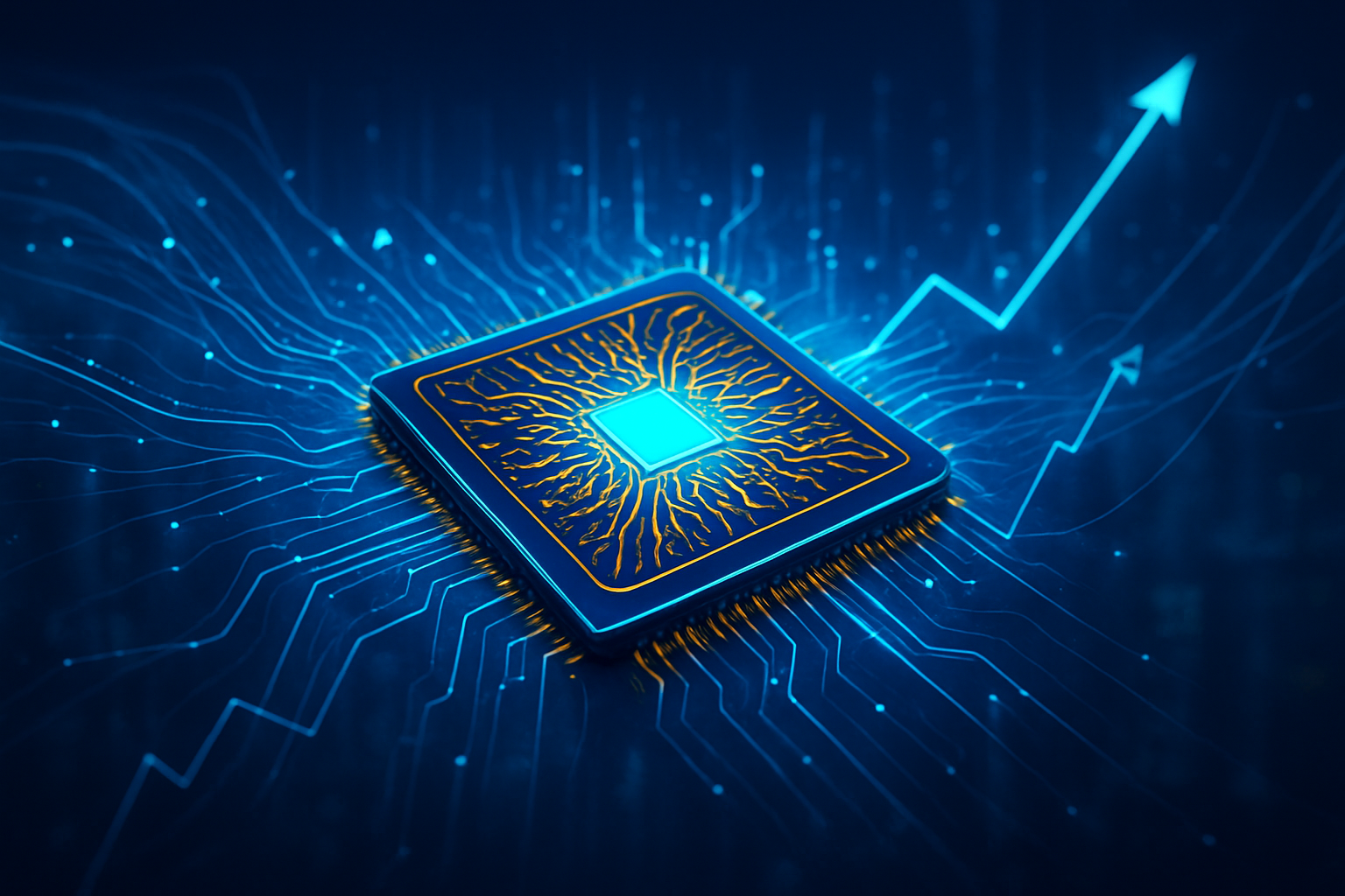
    The burgeoning field of Artificial Intelligence, particularly the explosive growth of large language models (LLMs) and generative AI, is fueling an unprecedented demand for advanced semiconductor solutions across nearly every technological sector. This symbiotic relationship sees AI's rapid advancements necessitating more sophisticated and specialized chips, while these cutting-edge semiconductors, in turn, unlock even greater AI capabilities. This pivotal trend is not merely an incremental shift but a fundamental reordering of priorities within the global technology landscape, marking AI as the undisputed primary engine of growth for the semiconductor industry.

    The immediate significance of this phenomenon is profound, driving a "supercycle" in the semiconductor market with robust growth projections and intense capital expenditure. From powering vast data centers and cloud computing infrastructures to enabling real-time processing on edge devices like autonomous vehicles and smart sensors, the computational intensity of modern AI demands hardware far beyond traditional general-purpose processors. This necessitates a relentless pursuit of innovation in chip design and manufacturing, pushing the boundaries towards smaller process nodes and specialized architectures, ultimately reshaping the entire tech ecosystem.

    The Dawn of Specialized AI Silicon: Technical Deep Dive

    The current wave of AI, characterized by its complexity and data-intensive nature, has fundamentally transformed the requirements for semiconductor hardware. Unlike previous computing paradigms that largely relied on general-purpose Central Processing Units (CPUs), modern AI workloads, especially deep learning and neural networks, thrive on parallel processing capabilities. This has propelled Graphics Processing Units (GPUs) into the spotlight as the workhorse of AI, with companies like Nvidia (NASDAQ: NVDA) pioneering architectures specifically optimized for AI computations.

    However, the evolution doesn't stop at GPUs. The industry is rapidly moving towards even more specialized Application-Specific Integrated Circuits (ASICs) and Neural Processing Units (NPUs). These custom-designed chips are engineered from the ground up to execute specific AI algorithms with unparalleled efficiency, offering significant advantages in terms of speed, power consumption, and cost-effectiveness for large-scale deployments. For instance, an NPU might integrate dedicated tensor cores or matrix multiplication units that can perform thousands of operations simultaneously, a capability far exceeding traditional CPU cores. This contrasts sharply with older approaches where AI tasks were shoehorned onto general-purpose hardware, leading to bottlenecks and inefficiencies.

    Technical specifications now often highlight parameters like TeraFLOPS (Trillions of Floating Point Operations Per Second) for AI workloads, memory bandwidth (with High Bandwidth Memory or HBM becoming standard), and interconnect speeds (e.g., NVLink, CXL). These metrics are critical for handling the immense datasets and complex model parameters characteristic of LLMs. The shift represents a departure from the "one-size-fits-all" computing model towards a highly fragmented and specialized silicon ecosystem, where each AI application demands tailored hardware. Initial reactions from the AI research community have been overwhelmingly positive, recognizing that these hardware advancements are crucial for pushing the boundaries of what AI can achieve, enabling larger models, faster training, and more sophisticated inference at scale.

    Reshaping the Competitive Landscape: Impact on Tech Giants and Startups

    The insatiable demand for advanced AI semiconductors is profoundly reshaping the competitive dynamics across the tech industry, creating clear winners and presenting significant challenges for others. Companies at the forefront of AI chip design and manufacturing, such as Nvidia (NASDAQ: NVDA), TSMC (NYSE: TSM), and Samsung (KRX: 005930), stand to benefit immensely. Nvidia, in particular, has cemented its position as a dominant force, with its GPUs becoming the de facto standard for AI training and inference. Its CUDA platform further creates a powerful ecosystem lock-in, making it challenging for competitors to gain ground.

    Tech giants like Google (NASDAQ: GOOGL), Amazon (NASDAQ: AMZN), and Microsoft (NASDAQ: MSFT) are also heavily investing in custom AI silicon to power their cloud services and reduce reliance on external suppliers. Google's Tensor Processing Units (TPUs), Amazon's Inferentia and Trainium chips, and Microsoft's Athena project are prime examples of this strategic pivot. This internal chip development offers these companies competitive advantages by optimizing hardware-software co-design, leading to superior performance and cost efficiencies for their specific AI workloads. This trend could potentially disrupt the market for off-the-shelf AI accelerators, challenging smaller startups that might struggle to compete with the R&D budgets and manufacturing scale of these behemoths.

    For startups specializing in AI, the landscape is both opportunistic and challenging. Those developing innovative AI algorithms or applications benefit from the availability of more powerful hardware, enabling them to bring sophisticated solutions to market. However, the high cost of accessing cutting-edge AI compute resources can be a barrier. Companies that can differentiate themselves with highly optimized software that extracts maximum performance from existing hardware, or those developing niche AI accelerators for specific use cases (e.g., neuromorphic computing, quantum-inspired AI), might find strategic advantages. The market positioning is increasingly defined by access to advanced silicon, making partnerships with semiconductor manufacturers or cloud providers with proprietary chips crucial for sustained growth and innovation.

    Wider Significance: A New Era of AI Innovation and Challenges

    The escalating demand for advanced semiconductors driven by AI fits squarely into the broader AI landscape as a foundational trend, underscoring the critical interplay between hardware and software in achieving next-generation intelligence. This development is not merely about faster computers; it's about enabling entirely new paradigms of AI that were previously computationally infeasible. It facilitates the creation of larger, more complex models with billions or even trillions of parameters, leading to breakthroughs in natural language understanding, computer vision, and generative capabilities that are transforming industries from healthcare to entertainment.

    The impacts are far-reaching. On one hand, it accelerates scientific discovery and technological innovation, empowering researchers and developers to tackle grand challenges. On the other hand, it raises potential concerns. The immense energy consumption of AI data centers, fueled by these powerful chips, poses environmental challenges and necessitates a focus on energy-efficient designs. Furthermore, the concentration of advanced semiconductor manufacturing, primarily in a few regions, exacerbates geopolitical tensions and creates supply chain vulnerabilities, as seen in recent global chip shortages.

    Compared to previous AI milestones, such as the advent of expert systems or early machine learning algorithms, the current hardware-driven surge is distinct in its scale and the fundamental re-architecture it demands. While earlier AI advancements often relied on algorithmic breakthroughs, today's progress is equally dependent on the ability to process vast quantities of data at unprecedented speeds. This era marks a transition where hardware is no longer just an enabler but an active co-developer of AI capabilities, pushing the boundaries of what AI can learn, understand, and create.

    The Horizon: Future Developments and Uncharted Territories

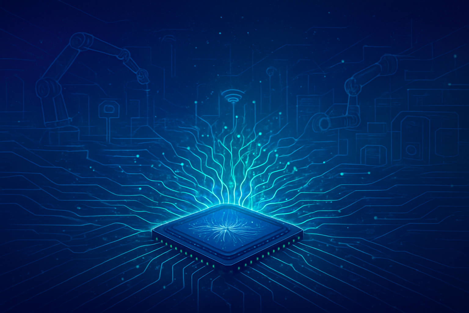
    Looking ahead, the trajectory of AI's influence on semiconductor development promises even more profound transformations. In the near term, we can expect continued advancements in process technology, with manufacturers like TSMC (NYSE: TSM) pushing towards 2nm and even 1.4nm nodes, enabling more transistors in smaller, more power-efficient packages. There will also be a relentless focus on increasing memory bandwidth and integrating heterogeneous computing elements, where different types of processors (CPUs, GPUs, NPUs, FPGAs) work seamlessly together within a single system or even on a single chip. Chiplet architectures, which allow for modular design and integration of specialized components, are also expected to become more prevalent, offering greater flexibility and scalability.

    Longer-term developments could see the rise of entirely new computing paradigms. Neuromorphic computing, which seeks to mimic the structure and function of the human brain, holds the promise of ultra-low-power, event-driven AI processing, moving beyond traditional Von Neumann architectures. Quantum computing, while still in its nascent stages, could eventually offer exponential speedups for certain AI algorithms, though its practical application for mainstream AI is likely decades away. Potential applications on the horizon include truly autonomous agents capable of complex reasoning, personalized medicine driven by AI-powered diagnostics on compact devices, and highly immersive virtual and augmented reality experiences rendered in real-time by advanced edge AI chips.

    However, significant challenges remain. The "memory wall" – the bottleneck between processing units and memory – continues to be a major hurdle, prompting innovations like in-package memory and advanced interconnects. Thermal management for increasingly dense and powerful chips is another critical engineering challenge. Furthermore, the software ecosystem needs to evolve rapidly to fully leverage these new hardware capabilities, requiring new programming models and optimization techniques. Experts predict a future where AI and semiconductor design become even more intertwined, with AI itself playing a greater role in designing the next generation of AI chips, creating a virtuous cycle of innovation.

    A New Silicon Renaissance: AI's Enduring Legacy

    In summary, the pivotal role of AI in driving the demand for advanced semiconductor solutions marks a new renaissance in the silicon industry. This era is defined by an unprecedented push for specialized, high-performance, and energy-efficient chips tailored for the computationally intensive demands of modern AI, particularly large language models and generative AI. Key takeaways include the shift from general-purpose to specialized accelerators (GPUs, ASICs, NPUs), the strategic imperative for tech giants to develop proprietary silicon, and the profound impact on global supply chains and geopolitical dynamics.

    This development's significance in AI history cannot be overstated; it represents a fundamental hardware-software co-evolution that is unlocking capabilities previously confined to science fiction. It underscores that the future of AI is inextricably linked to the continuous innovation in semiconductor technology. The long-term impact will likely see a more intelligent, interconnected world, albeit one that must grapple with challenges related to energy consumption, supply chain resilience, and the ethical implications of increasingly powerful AI.

    In the coming weeks and months, industry watchers should keenly observe the progress in sub-2nm process nodes, the commercialization of novel architectures like chiplets and neuromorphic designs, and the strategic partnerships and acquisitions in the semiconductor space. The race to build the most efficient and powerful AI hardware is far from over, and its outcomes will undoubtedly shape the technological landscape for decades to come.


    This content is intended for informational purposes only and represents analysis of current AI developments.

    TokenRing AI delivers enterprise-grade solutions for multi-agent AI workflow orchestration, AI-powered development tools, and seamless remote collaboration platforms.
    For more information, visit https://www.tokenring.ai/.

  • USMCA Review Puts North America’s AI Backbone to the Test: Global Electronics Association Sounds Alarm

    USMCA Review Puts North America’s AI Backbone to the Test: Global Electronics Association Sounds Alarm

    The intricate dance between global trade policies and the rapidly evolving technology sector is once again taking center stage as the United States-Mexico-Canada Agreement (USMCA) approaches its critical six-year joint review. On Thursday, December 4, 2025, a pivotal public hearing organized by the Office of the U.S. Trade Representative (USTR) will feature testimony from the Global Electronics Association (GEA), formerly IPC, highlighting the profound influence of these trade policies on the global electronics and semiconductor industry. This hearing, and the broader review slated for July 1, 2026, are not mere bureaucratic exercises; they represent a high-stakes negotiation that will shape the future of North American competitiveness, supply chain resilience, and critically, the foundational infrastructure for artificial intelligence development and deployment.

    The GEA's testimony, led by Vice President for Global Government Relations Chris Mitchell, will underscore the imperative of strengthening North American supply chains and fostering cross-border collaboration. With the electronics sector being the most globally integrated industry, the outcomes of this review will directly impact the cost, availability, and innovation trajectory of the semiconductors and components that power every AI system, from large language models to autonomous vehicles. The stakes are immense, as the decisions made in the coming months will determine whether North America solidifies its position as a technological powerhouse or succumbs to fragmented policies that could stifle innovation and increase dependencies.

    Navigating the Nuances of North American Trade: Rules of Origin and Resilience

    The USMCA, which superseded NAFTA in 2020, introduced a dynamic framework designed to modernize trade relations and bolster regional manufacturing. At the heart of the GEA's testimony and the broader review are the intricate details of trade policy, particularly the "rules of origin" (ROO) for electronics and semiconductors. These rules dictate whether a product qualifies for duty-free entry within the USMCA region, typically through a "tariff shift" (a change in tariff classification during regional production) or by meeting a "Regional Value Content" (RVC) threshold (e.g., 60% by transaction value or 50% by net cost originating from the USMCA region).

    The GEA emphasizes that for complex, high-value manufacturing processes in the electronics sector, workable rules of origin are paramount. While the USMCA aims to incentivize regional content, the electronics industry relies on a globally distributed supply chain for specialized components. The GEA's stance, articulated in its October 2025 policy brief "From Risk to Resilience: Why Mexico Matters to U.S. Manufacturing," advocates for "resilience, not self-sufficiency." This perspective subtly challenges protectionist rhetoric that might push for complete "reshoring" at the expense of efficient, integrated North American supply chains. The Association warns that overly stringent ROO or the imposition of new penalties, such as proposed 30% tariffs on electronics imports from Mexico, could "fracture supply chains, increase costs for U.S. manufacturers, and undermine reshoring efforts." This nuanced approach reinforces the benefits of a predictable, rules-based framework while cautioning against measures that could disrupt legitimate cross-border production essential for global competitiveness. The discussion around ROO for advanced components, particularly in the context of final assembly, testing, and packaging (FATP) in Mexico or Canada, highlights the technical complexities of defining "North American" content for cutting-edge technology.

    Initial reactions from the AI research community and industry experts largely echo the GEA's call for stability and integrated supply chains. The understanding is that any disruption to the flow of semiconductors and electronic components directly impacts the ability to build, train, and deploy AI models. While there's a desire for greater domestic production, the immediate priority for many is predictability and efficiency, which the USMCA, if properly managed, can provide.

    Corporate Crossroads: Winners, Losers, and Strategic Shifts in the AI Era

    The outcomes of the USMCA review will reverberate across the corporate landscape, creating both beneficiaries and those facing significant headwinds, particularly within the electronics, semiconductor, and AI industries.

    Beneficiaries largely include companies that have strategically invested in or are planning to expand manufacturing and assembly operations within the U.S., Mexico, and Canada. The USMCA's incentives for regional content have already spurred a "nearshoring" boom, with companies like Foxconn (TWSE: 2317), Pegatron (TWSE: 4938), and Quanta Computer (TWSE: 2382) reportedly shifting AI-focused production, such as AI server assembly, to Mexico. This move mitigates geopolitical and logistics risks associated with distant supply chains and leverages the agreement's tariff-free benefits. Semiconductor manufacturers with existing or planned facilities in North America also stand to gain, especially as the U.S. CHIPS Act complements USMCA efforts to bolster regional chip production. Companies whose core value lies in intellectual property (IP), such as major AI labs and tech giants, benefit from the USMCA's robust IP protections, which safeguard proprietary algorithms, source code, and data. The agreement's provisions for free cross-border data flows are also crucial for hyperscalers and AI developers who rely on vast datasets for training.

    Conversely, companies heavily reliant on non-North American supply chains for components or final assembly could face negative impacts. Stricter rules of origin or the imposition of new tariffs, as warned by the GEA, could increase production costs, necessitate costly supply chain restructuring, or even lead to product redesigns. This could disrupt existing product lines and make goods more expensive for consumers. Furthermore, companies that have not adequately adapted to the USMCA's labor and environmental standards in Mexico might face increased operational costs.

    The competitive implications are significant. For major AI labs and established tech companies, continued stability under USMCA provides a strategic advantage for supply chain resilience and protects their digital assets. However, they must remain vigilant for potential shifts in data privacy regulations or new tariffs. Startups in hardware (electronics, semiconductors) might find navigating complex ROO challenging, potentially increasing their costs. Yet, the USMCA's digital trade chapter aims to facilitate e-commerce for SMEs, potentially opening new investment opportunities for AI-powered service startups. The GEA's warnings about tariffs underscore the potential for significant market disruption, as fractured supply chains would inevitably lead to higher costs for consumers and reduced competitiveness for U.S. manufacturers in the global market.

    Beyond Borders: USMCA's Role in the Global AI Race and Geopolitical Chessboard

    The USMCA review extends far beyond regional trade, embedding itself within the broader AI landscape and current global tech trends. Stable electronics and semiconductor supply chains, nurtured by effective trade agreements, are not merely an economic convenience; they are the foundational bedrock upon which AI development and deployment are built. Advanced AI systems, from sophisticated large language models to cutting-edge robotics, demand an uninterrupted supply of high-performance semiconductors, including GPUs and TPUs. Disruptions in this critical supply chain, as witnessed during recent global crises, can severely impede AI progress, causing delays, increasing costs, and ultimately slowing the pace of innovation.

    The USMCA's provisions, particularly those fostering regional integration and predictable rules of origin, are thus strategic assets in the global AI race. By encouraging domestic and near-shore manufacturing, the agreement aims to reduce reliance on potentially volatile distant supply chains, enhancing North America's resilience against external shocks. This strategic alignment is particularly relevant as nations vie for technological supremacy in advanced manufacturing and digital services. The GEA's advocacy for "resilience, not self-sufficiency" resonates with the practicalities of a globally integrated industry while still aiming to secure regional advantages.

    However, the review also brings forth significant concerns. Data privacy is paramount in the age of AI, where systems are inherently data-intensive. While USMCA facilitates cross-border data flows, there's a growing call for enhanced data privacy standards that protect individuals without stifling AI innovation. The specter of "data nationalism" and fragmented regulatory landscapes across member states could complicate international AI development. Geopolitical implications loom large, with the "AI race" influencing trade policies and nations seeking to secure leadership in critical technologies. The review occurs amidst a backdrop of strategic competition, where some nations implement export restrictions on advanced chipmaking technologies. This can lead to higher prices, reduced innovation, and a climate of uncertainty, impacting the global tech sector.

    Comparing this to past milestones, the USMCA itself replaced NAFTA, introducing a six-year review mechanism that acknowledges the need for trade agreements to adapt to rapid technological change – a significant departure from older, more static agreements. The explicit inclusion of digital trade clauses, cross-border data flows, and IP protection for digital goods marks a clear evolution from agreements primarily focused on physical goods, reflecting the increasing digitalization of the global economy. This shift parallels historical "semiconductor wars," where trade policy was strategically wielded to protect domestic industries, but with the added complexity of AI's pervasive role across all modern sectors.

    The Horizon of Innovation: Future Developments and Expert Outlook

    The USMCA review, culminating in the formal joint review in July 2026, sets the stage for several crucial near-term and long-term developments that will profoundly influence the global electronics, semiconductor, and AI industries.

    In the near term, the immediate focus will be on the 2026 joint review itself. A successful extension for another 16-year term is critical to prevent business uncertainty and maintain investment momentum. Key areas of negotiation will likely include further strengthening intellectual property enforcement, particularly for AI-generated works, and modernizing digital trade provisions to accommodate rapidly evolving AI technologies. Mexico's proposal for a dedicated semiconductor chapter within the USMCA signifies a strong regional ambition to align industrial policy with geopolitical tech shifts, aiming to boost domestic production and reduce reliance on Asian imports. The Semiconductor Industry Association (SIA) has also advocated for tariff-free treatment for North American semiconductors and robust rules of origin to incentivize regional investment.

    Looking further into the long term, a successful USMCA extension could pave the way for a more deeply integrated North American economic bloc, particularly in advanced manufacturing and digital industries. Experts predict a continued trend of reshoring and nearshoring for critical components, bolstering supply chain resilience. This will likely involve deepening cooperation in strategic sectors like critical minerals, electric vehicles, and advanced technology, with AI playing an increasingly central role in optimizing these processes. Developing a common approach to AI regulation, privacy policies, and cybersecurity across North America will be paramount to foster a collaborative AI ecosystem and enable seamless data flows.

    Potential applications and use cases on the horizon, fueled by stable trade policies, include advanced AI-enhanced manufacturing systems integrating operations across the U.S., Mexico, and Canada. This encompasses predictive supply chain analytics, optimized inventory management, and automated quality control. Facilitated cross-border data flows will enable more sophisticated AI development and deployment, leading to innovative data-driven services and products across the region.

    However, several challenges need to be addressed. Regulatory harmonization remains a significant hurdle, as divergent AI regulations and data privacy policies across the three nations could create costly compliance burdens and hinder digital trade. Workforce development is another critical concern, with the tech sector, especially semiconductors and AI, facing a substantial skills gap. Coordinated regional strategies for training and increasing the mobility of AI talent are essential. The ongoing tension between data localization demands and the USMCA's promotion of free data flow, along with the need for robust intellectual property protections for AI algorithms within the current framework, will require careful navigation. Finally, geopolitical pressures and the potential for tariffs stemming from non-trade issues could introduce volatility, while infrastructure gaps, particularly in Mexico, need to be addressed to fully realize nearshoring potential.

    Experts generally predict that the 2026 USMCA review will be a pivotal moment to update the agreement for the AI-driven economy. While an extension is likely, it's not guaranteed without concessions. There will be a strong emphasis on integrating AI into trade policies, continued nearshoring of AI hardware manufacturing to Mexico, and persistent efforts towards regulatory harmonization. The political dynamics in all three countries will play a crucial role in shaping the final outcome.

    The AI Age's Trade Imperative: A Comprehensive Wrap-Up

    The upcoming USMCA review hearing and the Global Electronics Association's testimony mark a crucial juncture for the future of North American trade, with profound implications for the global electronics, semiconductor, and Artificial Intelligence industries. The core takeaway is clear: stable, predictable, and resilient supply chains are not just an economic advantage but a fundamental necessity for the advancement of AI. The GEA's advocacy for "resilience, not self-sufficiency" underscores the complex, globally integrated nature of the electronics sector and the need for policies that foster collaboration rather than fragmentation.

    This development's significance in AI history cannot be overstated. As AI continues its rapid ascent, becoming the driving force behind economic growth and technological innovation, the underlying hardware and data infrastructure must be robust and reliable. The USMCA, with its provisions on digital trade, intellectual property, and regional content, offers a framework to achieve this, but its ongoing review presents both opportunities to strengthen these foundations and risks of undermining them through protectionist measures or regulatory divergence.

    In the long term, the outcome of this review will determine North America's competitive standing in the global AI race. A successful, modernized USMCA can accelerate nearshoring, foster a collaborative AI ecosystem, and ensure a steady supply of critical components. Conversely, a failure to adapt the agreement to the realities of the AI age, or the imposition of disruptive trade barriers, could lead to increased costs, stunted innovation, and a reliance on less stable supply chains.

    What to watch for in the coming weeks and months includes the specific recommendations emerging from the December 4th hearing, the USTR's subsequent reports, and the ongoing dialogue among the U.S., Mexico, and Canada leading up to the July 2026 joint review. The evolution of discussions around a dedicated semiconductor chapter and efforts towards harmonizing AI regulations across the region will be key indicators of North America's commitment to securing its technological future.


    This content is intended for informational purposes only and represents analysis of current AI developments.

    TokenRing AI delivers enterprise-grade solutions for multi-agent AI workflow orchestration, AI-powered development tools, and seamless remote collaboration platforms.
    For more information, visit https://www.tokenring.ai/.

  • Bank of America Doubles Down: Why Wall Street Remains Bullish on AI Semiconductor Titans Nvidia, AMD, and Broadcom

    Bank of America Doubles Down: Why Wall Street Remains Bullish on AI Semiconductor Titans Nvidia, AMD, and Broadcom

    In a resounding vote of confidence for the artificial intelligence revolution, Bank of America (NYSE: BAC) has recently reaffirmed its "Buy" ratings for three of the most pivotal players in the AI semiconductor landscape: Nvidia (NASDAQ: NVDA), Advanced Micro Devices (NASDAQ: AMD), and Broadcom (NASDAQ: AVGO). This significant endorsement, announced around November 25-26, 2025, just days before the current date of December 1, 2025, underscores a robust and sustained bullish sentiment from the financial markets regarding the continued, explosive growth of the AI sector. The move signals to investors that despite market fluctuations and intensifying competition, the foundational hardware providers for AI are poised for substantial long-term gains, driven by an insatiable global demand for advanced computing power.

    The immediate significance of Bank of America's reaffirmation lies in its timing and the sheer scale of the projected market growth. With the AI data center market anticipated to balloon fivefold from an estimated $242 billion in 2025 to a staggering $1.2 trillion by the end of the decade, the financial institution sees a rising tide that will undeniably lift the fortunes of these semiconductor giants. This outlook provides a crucial anchor of stability and optimism in an otherwise dynamic tech landscape, reassuring investors about the fundamental strength and expansion trajectory of AI infrastructure. The sustained demand for AI chips, fueled by robust investments in cloud infrastructure, advanced analytics, and emerging AI applications, forms the bedrock of this confident market stance, reinforcing the notion that the AI boom is not merely a transient trend but a profound, enduring technological shift.

    The Technical Backbone of the AI Revolution: Decoding Chip Dominance

    The bullish sentiment surrounding Nvidia, AMD, and Broadcom is deeply rooted in their unparalleled technical contributions to the AI ecosystem. Each company plays a distinct yet critical role in powering the complex computations that underpin modern artificial intelligence.

    Nvidia, the undisputed leader in AI GPUs, continues to set the benchmark with its specialized architectures designed for parallel processing, a cornerstone of deep learning and neural networks. Its CUDA software platform, a proprietary parallel computing architecture, along with an extensive suite of developer tools, forms a comprehensive ecosystem that has become the industry standard for AI development and deployment. This deep integration of hardware and software creates a formidable moat, making it challenging for competitors to replicate Nvidia's end-to-end solution. The company's GPUs, such as the H100 and upcoming next-generation accelerators, offer unparalleled performance for training large language models (LLMs) and executing complex AI inferences, distinguishing them from traditional CPUs that are less efficient for these specific workloads.

    Advanced Micro Devices (AMD) is rapidly emerging as a formidable challenger, expanding its footprint across CPU, GPU, embedded, and gaming segments, with a particular focus on the high-growth AI accelerator market. AMD's Instinct MI series accelerators are designed to compete directly with Nvidia's offerings, providing powerful alternatives for AI workloads. The company's strategy often involves open-source software initiatives, aiming to attract developers seeking more flexible and less proprietary solutions. While historically playing catch-up in the AI GPU space, AMD's aggressive product roadmap and diversified portfolio position it to capture a significant double-digit percentage of the AI accelerator market, offering compelling performance-per-dollar propositions.

    Broadcom, while not as directly visible in consumer-facing AI as its GPU counterparts, is a critical enabler of the AI infrastructure through its expertise in networking and custom AI chips (ASICs). The company's high-performance switching and routing solutions are essential for the massive data movement within hyperscale data centers, which are the powerhouses of AI. Furthermore, Broadcom's role as a co-manufacturer and designer of application-specific integrated circuits, notably for Google's (NASDAQ: GOOGL) Tensor Processing Units (TPUs) and other specialized AI projects, highlights its strategic importance. These custom ASICs are tailored for specific AI workloads, offering superior efficiency and performance for particular tasks, differentiating them from general-purpose GPUs and providing a crucial alternative for tech giants seeking optimized, proprietary solutions.

    Competitive Implications and Strategic Advantages in the AI Arena

    The sustained strength of the AI semiconductor market, as evidenced by Bank of America's bullish outlook, has profound implications for AI companies, tech giants, and startups alike, shaping the competitive landscape and driving strategic decisions.

    Cloud service providers like Amazon (NASDAQ: AMZN) Web Services, Microsoft (NASDAQ: MSFT) Azure, and Google Cloud stand to benefit immensely from the advancements and reliable supply of these high-performance chips. Their ability to offer cutting-edge AI infrastructure directly depends on access to Nvidia's GPUs, AMD's accelerators, and Broadcom's networking solutions. This dynamic creates a symbiotic relationship where the growth of cloud AI services fuels demand for these semiconductors, and in turn, the availability of advanced chips enables cloud providers to offer more powerful and sophisticated AI tools to their enterprise clients and developers.

    For major AI labs and tech companies, the competition for these critical components intensifies. Access to the latest and most powerful chips can determine the pace of innovation, the scale of models that can be trained, and the efficiency of AI inference at scale. This often leads to strategic partnerships, long-term supply agreements, and even in-house chip development efforts, as seen with Google's TPUs, co-designed with Broadcom, and Meta Platforms' (NASDAQ: META) exploration of various AI hardware options. The market positioning of Nvidia, AMD, and Broadcom directly influences the competitive advantage of these AI developers, as superior hardware can translate into faster model training, lower operational costs, and ultimately, more advanced AI products and services.

    Startups in the AI space, particularly those focused on developing novel AI applications or specialized models, are also significantly affected. While they might not purchase chips in the same volume as hyperscalers, their ability to access powerful computing resources, often through cloud platforms, is paramount. The continued innovation and availability of efficient AI chips enable these startups to scale their operations, conduct research, and bring their solutions to market more effectively. However, the high cost of advanced AI hardware can also present a barrier to entry, potentially consolidating power among well-funded entities and cloud providers. The market for AI semiconductors is not just about raw power but also about democratizing access to that power, which has implications for the diversity and innovation within the AI startup ecosystem.

    The Broader AI Landscape: Trends, Impacts, and Future Considerations

    Bank of America's confident stance on AI semiconductor stocks reflects and reinforces a broader trend in the AI landscape: the foundational importance of hardware in unlocking the full potential of artificial intelligence. This focus on the "picks and shovels" of the AI gold rush highlights that while algorithmic advancements and software innovations are crucial, they are ultimately bottlenecked by the underlying computing power.

    The impact extends far beyond the tech sector, influencing various industries from healthcare and finance to manufacturing and autonomous systems. The ability to process vast datasets and run complex AI models with greater speed and efficiency translates into faster drug discovery, more accurate financial predictions, optimized supply chains, and safer autonomous vehicles. However, this intense demand also raises potential concerns, particularly regarding the environmental impact of energy-intensive AI data centers and the geopolitical implications of a concentrated semiconductor supply chain. The "chip battle" also underscores national security interests and the drive for technological sovereignty among major global powers.

    Compared to previous AI milestones, such as the advent of expert systems or early neural networks, the current era is distinguished by the unprecedented scale of data and computational requirements. The breakthroughs in large language models and generative AI, for instance, would be impossible without the massive parallel processing capabilities offered by modern GPUs and ASICs. This era signifies a transition where AI is no longer a niche academic pursuit but a pervasive technology deeply integrated into the global economy. The reliance on a few key semiconductor providers for this critical infrastructure draws parallels to previous industrial revolutions, where control over foundational resources conferred immense power and influence.

    The Horizon of Innovation: Future Developments in AI Semiconductors

    Looking ahead, the trajectory of AI semiconductor development promises even more profound advancements, pushing the boundaries of what's currently possible and opening new frontiers for AI applications.

    Near-term developments are expected to focus on further optimizing existing architectures, such as increasing transistor density, improving power efficiency, and enhancing interconnectivity between chips within data centers. Companies like Nvidia and AMD are continuously refining their GPU designs, while Broadcom will likely continue its work on custom ASICs and high-speed networking solutions to reduce latency and boost throughput. We can anticipate the introduction of next-generation AI accelerators with significantly higher processing power and memory bandwidth, specifically tailored for ever-larger and more complex AI models.

    Longer-term, the industry is exploring revolutionary computing paradigms beyond the traditional Von Neumann architecture. Neuromorphic computing, which seeks to mimic the structure and function of the human brain, holds immense promise for energy-efficient and highly parallel AI processing. While still in its nascent stages, breakthroughs in this area could dramatically alter the landscape of AI hardware. Similarly, quantum computing, though further out on the horizon, could eventually offer exponential speedups for certain AI algorithms, particularly in areas like optimization and material science. Challenges that need to be addressed include overcoming the physical limitations of silicon-based transistors, managing the escalating power consumption of AI data centers, and developing new materials and manufacturing processes.

    Experts predict a continued diversification of AI hardware, with a move towards more specialized and heterogeneous computing environments. This means a mix of general-purpose GPUs, custom ASICs, and potentially neuromorphic chips working in concert, each optimized for different aspects of AI workloads. The focus will shift not just to raw computational power but also to efficiency, programmability, and ease of integration into complex AI systems. What's next is a race for not just faster chips, but smarter, more sustainable, and more versatile AI hardware.

    A New Era of AI Infrastructure: The Enduring Significance

    Bank of America's reaffirmation of "Buy" ratings for Nvidia, AMD, and Broadcom serves as a powerful testament to the enduring significance of semiconductor technology in the age of artificial intelligence. The key takeaway is clear: the AI boom is robust, and the companies providing its essential hardware infrastructure are poised for sustained growth. This development is not merely a financial blip but a critical indicator of the deep integration of AI into the global economy, driven by an insatiable demand for processing power.

    This moment marks a pivotal point in AI history, highlighting the transition from theoretical advancements to widespread, practical application. The ability of these companies to continuously innovate and scale their production of high-performance chips is directly enabling the breakthroughs we see in large language models, autonomous systems, and a myriad of other AI-powered technologies. The long-term impact will be a fundamentally transformed global economy, where AI-driven efficiency and innovation becomes the norm, rather than the exception.

    In the coming weeks and months, investors and industry observers alike should watch for continued announcements regarding new chip architectures, expanded manufacturing capabilities, and strategic partnerships. The competitive dynamics between Nvidia, AMD, and Broadcom will remain a key area of focus, as each strives to capture a larger share of the rapidly expanding AI market. Furthermore, the broader implications for energy consumption and supply chain resilience will continue to be important considerations as the world becomes increasingly reliant on this foundational technology. The future of AI is being built, transistor by transistor, and these three companies are at the forefront of that construction.


    This content is intended for informational purposes only and represents analysis of current AI developments.

    TokenRing AI delivers enterprise-grade solutions for multi-agent AI workflow orchestration, AI-powered development tools, and seamless remote collaboration platforms.
    For more information, visit https://www.tokenring.ai/.

  • Nvidia Supercharges AI Chip Design with $2 Billion Synopsys Investment: A New Era for Accelerated Engineering

    Nvidia Supercharges AI Chip Design with $2 Billion Synopsys Investment: A New Era for Accelerated Engineering

    In a groundbreaking move set to redefine the landscape of AI chip development, NVIDIA (NASDAQ: NVDA) has announced a strategic partnership with Synopsys (NASDAQ: SNPS), solidified by a substantial $2 billion investment in Synopsys common stock. This multi-year collaboration, unveiled on December 1, 2025, is poised to revolutionize engineering and design across a multitude of industries, with its most profound impact expected in accelerating the innovation cycle for artificial intelligence chips. The immediate significance of this colossal investment lies in its potential to dramatically fast-track the creation of next-generation AI hardware, fundamentally altering how complex AI systems are conceived, designed, and brought to market.

    The partnership aims to integrate NVIDIA's unparalleled prowess in AI and accelerated computing with Synopsys's market-leading electronic design automation (EDA) solutions and deep engineering expertise. By merging these capabilities, the alliance is set to unlock unprecedented efficiencies in compute-intensive applications crucial for chip design, physical verification, and advanced simulations. This strategic alignment underscores NVIDIA's commitment to deepening its footprint across the entire AI ecosystem, ensuring a robust foundation for the continued demand and evolution of its cutting-edge AI hardware.

    Redefining the Blueprint: Technical Deep Dive into Accelerated AI Chip Design

    The $2 billion investment sees NVIDIA acquiring approximately 2.6% of Synopsys's shares at $414.79 per share, making it a significant stakeholder. This private placement signals a profound commitment to leveraging Synopsys's critical role in the semiconductor design process. Synopsys's EDA tools are the backbone of modern chip development, enabling engineers to design, simulate, and verify the intricate layouts of integrated circuits before they are ever fabricated. The technical crux of this partnership involves Synopsys integrating NVIDIA’s CUDA-X™ libraries and AI physics technologies directly into its extensive portfolio of compute-intensive applications. This integration promises to dramatically accelerate workflows in areas such as chip design, physical verification, molecular simulations, electromagnetic analysis, and optical simulation, potentially reducing tasks that once took weeks to mere hours.

    A key focus of this collaboration is the advancement of "agentic AI engineering." This cutting-edge approach involves deploying AI to automate and optimize complex design and engineering tasks, moving towards more autonomous and intelligent design processes. Specifically, Synopsys AgentEngineer technology will be integrated with NVIDIA’s robust agentic AI stack. This marks a significant departure from traditional, largely human-driven chip design methodologies. Previously, engineers relied heavily on manual iterations and computationally intensive simulations on general-purpose CPUs. The NVIDIA-Synopsys synergy introduces GPU-accelerated computing and AI-driven automation, promising to not only speed up existing processes but also enable the exploration of design spaces previously inaccessible due to time and computational constraints.

    Furthermore, the partnership aims to expand cloud access for joint solutions and develop Omniverse digital twins. These virtual representations of real-world assets will enable simulation at unprecedented speed and scale, spanning from atomic structures to transistors, chips, and entire systems. This capability bridges the physical and digital realms, allowing for comprehensive testing and optimization in a virtual environment before physical prototyping, a critical advantage in complex AI chip development. Initial reactions from the AI research community and industry experts have been overwhelmingly positive, with many hailing it as a strategic masterstroke that will cement NVIDIA's leadership in AI hardware and significantly advance the capabilities of chip design itself. Experts anticipate a wave of innovation in chip architectures, driven by these newly accelerated design cycles.

    Reshaping the Competitive Landscape: Implications for AI Companies and Tech Giants

    This monumental investment and partnership carry profound implications for AI companies, tech giants, and startups across the industry. NVIDIA (NASDAQ: NVDA) stands to benefit immensely, solidifying its position not just as a leading provider of AI accelerators but also as a foundational enabler of the entire AI hardware development ecosystem. By investing in Synopsys, NVIDIA is directly enhancing the tools used to design the very chips that will demand its GPUs, effectively underwriting and accelerating the AI boom it relies upon. Synopsys (NASDAQ: SNPS), in turn, gains a significant capital injection and access to NVIDIA’s cutting-edge AI and accelerated computing expertise, further entrenching its market leadership in EDA tools and potentially opening new revenue streams through enhanced, AI-powered offerings.

    The competitive implications for other major AI labs and tech companies are substantial. Companies like Advanced Micro Devices (NASDAQ: AMD) and Intel (NASDAQ: INTC), both striving to capture a larger share of the AI chip market, will face an even more formidable competitor. NVIDIA’s move creates a deeper moat around its ecosystem, as accelerated design tools will likely lead to faster, more efficient development of NVIDIA-optimized hardware. Hyperscalers such as Amazon (NASDAQ: AMZN), Google (NASDAQ: GOOGL), and Microsoft (NASDAQ: MSFT), which are increasingly designing their own custom AI chips (e.g., AWS Inferentia, Google TPU, Microsoft Maia), will also feel the pressure. While Synopsys maintains that the partnership is non-exclusive, NVIDIA’s direct investment and deep technical collaboration could give it an implicit advantage in accessing and optimizing the most advanced EDA capabilities for its own hardware.

    This development has the potential to disrupt existing products and services by accelerating the obsolescence cycle of less efficient design methodologies. Startups in the AI chip space might find it easier to innovate with access to these faster, AI-augmented design tools, but they will also need to contend with the rapidly advancing capabilities of industry giants. Market positioning and strategic advantages will increasingly hinge on the ability to leverage accelerated design processes to bring high-performance, cost-effective AI hardware to market faster. NVIDIA’s investment reinforces its strategy of not just selling chips, but also providing the entire software and tooling stack that makes its hardware indispensable, creating a powerful flywheel effect for its AI dominance.

    Broader Significance: A Catalyst for AI's Next Frontier

    NVIDIA’s $2 billion bet on Synopsys represents a pivotal moment that fits squarely into the broader AI landscape and the accelerating trend of specialized AI hardware. As AI models grow exponentially in complexity and size, the demand for custom, highly efficient silicon designed specifically for AI workloads has skyrocketed. This partnership directly addresses the bottleneck in the AI hardware supply chain: the design and verification process itself. By infusing AI and accelerated computing into EDA, the collaboration is poised to unleash a new wave of innovation in chip architectures, enabling the creation of more powerful, energy-efficient, and specialized AI processors.

    The impacts of this development are far-reaching. It will likely lead to a significant reduction in the time-to-market for new AI chips, allowing for quicker iteration and deployment of advanced AI capabilities across various sectors, from autonomous vehicles and robotics to healthcare and scientific discovery. Potential concerns, however, include increased market consolidation within the AI chip design ecosystem. With NVIDIA deepening its ties to a critical EDA vendor, smaller players or those without similar strategic partnerships might face higher barriers to entry or struggle to keep pace with the accelerated innovation cycles. This could potentially lead to a more concentrated market for high-performance AI silicon.

    This milestone can be compared to previous AI breakthroughs that focused on software algorithms or model architectures. While those advancements pushed the boundaries of what AI could do, this investment directly addresses how the underlying hardware is built, which is equally fundamental. It signifies a recognition that further leaps in AI performance are increasingly dependent on innovations at the silicon level, and that the design process itself must evolve to meet these demands. It underscores a shift towards a more integrated approach, where hardware, software, and design tools are co-optimized for maximum AI performance.

    The Road Ahead: Anticipating Future Developments and Challenges

    Looking ahead, this partnership is expected to usher in several near-term and long-term developments. In the near term, we can anticipate a rapid acceleration in the development cycles for new AI chip designs. Companies utilizing Synopsys's GPU-accelerated tools, powered by NVIDIA's technology, will likely bring more complex and optimized AI silicon to market at an unprecedented pace. This could lead to a proliferation of specialized AI accelerators tailored for specific tasks, moving beyond general-purpose GPUs to highly efficient ASICs for niche AI applications. Long-term, the vision of "agentic AI engineering" could mature, with AI systems playing an increasingly autonomous role in the entire chip design process, from initial concept to final verification, potentially leading to entirely novel chip architectures that human designers might not conceive on their own.

    Potential applications and use cases on the horizon are vast. Faster chip design means faster innovation in areas like edge AI, where compact, power-efficient AI processing is crucial. It could also accelerate breakthroughs in scientific computing, drug discovery, and climate modeling, as the underlying hardware for complex simulations becomes more powerful and accessible. The development of Omniverse digital twins for chips and entire systems will enable unprecedented levels of pre-silicon validation and optimization, reducing costly redesigns and accelerating deployment in critical applications.

    However, several challenges need to be addressed. Scaling these advanced design methodologies to accommodate the ever-increasing complexity of future AI chips, while managing power consumption and thermal limits, remains a significant hurdle. Furthermore, ensuring seamless software integration between the new AI-powered design tools and existing workflows will be crucial for widespread adoption. Experts predict that the next few years will see a fierce race in AI hardware, with the NVIDIA-Synopsys partnership setting a new benchmark for design efficiency. The focus will shift from merely designing faster chips to designing smarter, more specialized, and more energy-efficient chips through intelligent automation.

    Comprehensive Wrap-up: A New Chapter in AI Hardware Innovation

    NVIDIA's $2 billion strategic investment in Synopsys marks a defining moment in the history of artificial intelligence hardware development. The key takeaway is the profound commitment to integrating AI and accelerated computing directly into the foundational tools of chip design, promising to dramatically shorten development cycles and unlock new frontiers of innovation. This partnership is not merely a financial transaction; it represents a synergistic fusion of leading-edge AI hardware and critical electronic design automation software, creating a powerful engine for the next generation of AI chips.

    Assessing its significance, this development stands as one of the most impactful strategic alliances in the AI ecosystem in recent years. It underscores the critical role that specialized hardware plays in advancing AI and highlights NVIDIA's proactive approach to shaping the entire supply chain to its advantage. By accelerating the design of AI chips, NVIDIA is effectively accelerating the future of AI itself. This move reinforces the notion that continued progress in AI will rely heavily on a holistic approach, where breakthroughs in algorithms are matched by equally significant advancements in the underlying computational infrastructure.

    Looking ahead, the long-term impact of this partnership will be the rapid evolution of AI hardware, leading to more powerful, efficient, and specialized AI systems across virtually every industry. What to watch for in the coming weeks and months will be the initial results of this technical collaboration: announcements of accelerated design workflows, new AI-powered features within Synopsys's EDA suite, and potentially, the unveiling of next-generation AI chips that bear the hallmark of this expedited design process. This alliance sets a new precedent for how technology giants will collaborate to push the boundaries of what's possible in artificial intelligence.


    This content is intended for informational purposes only and represents analysis of current AI developments.

    TokenRing AI delivers enterprise-grade solutions for multi-agent AI workflow orchestration, AI-powered development tools, and seamless remote collaboration platforms.
    For more information, visit https://www.tokenring.ai/.

  • Lattice Semiconductor: A Niche Powerhouse Poised for a Potential Double in Value Amidst the Edge AI Revolution

    Lattice Semiconductor: A Niche Powerhouse Poised for a Potential Double in Value Amidst the Edge AI Revolution

    In the rapidly evolving landscape of artificial intelligence, where computational demands are escalating, the spotlight is increasingly turning to specialized semiconductor companies that power the AI revolution at its very edge. Among these, Lattice Semiconductor Corporation (NASDAQ: LSCC) stands out as a compelling example of a niche player with significant growth potential, strategically positioned to capitalize on the burgeoning demand for low-power, high-performance programmable solutions. Industry analysts and market trends suggest that Lattice, with its focus on Field-Programmable Gate Arrays (FPGAs), could see its valuation double over the next five years, driven by the insatiable appetite for AI at the edge, IoT, and industrial automation.

    Lattice's trajectory is a testament to the power of specialization in a market often dominated by tech giants. By concentrating on critical, yet often overlooked, segments of the semiconductor industry, the company has carved out a unique and indispensable role. Its innovative FPGA technology is not just enabling current AI applications but is also laying the groundwork for future advancements, making it a crucial enabler for the next wave of intelligent devices and systems.

    The Technical Edge: Powering Intelligence Where It Matters Most

    Lattice Semiconductor's success is deeply rooted in its advanced technical offerings, primarily its portfolio of low-power FPGAs and comprehensive solution stacks. Unlike traditional CPUs or GPUs, which are designed for general-purpose computing or massive parallel processing respectively, Lattice's FPGAs offer unparalleled flexibility, low power consumption, and real-time processing capabilities crucial for edge applications. This differentiation is key in environments where latency, power budget, and physical footprint are paramount.

    The company's flagship platforms, Lattice Nexus and Lattice Avant, exemplify its commitment to innovation. The Nexus platform, tailored for small FPGAs, provides a robust foundation for compact and energy-efficient designs. Building on this, the Lattice Avant™ platform, introduced in 2022, significantly expanded the company's addressable market by targeting mid-range FPGAs. Notably, the Avant-E family is specifically engineered for low-power edge computing, boasting package sizes as small as 11 mm x 9 mm and consuming 2.5 times less power than comparable devices from competitors. This technical prowess allows for the deployment of sophisticated AI inference directly on edge devices, bypassing the need for constant cloud connectivity and addressing critical concerns like data privacy and real-time responsiveness.

    Lattice's product diversity, including general-purpose FPGAs like CertusPro-NX, video connection FPGAs such as CrossLink-NX, and ultra-low power FPGAs like iCE40 UltraPlus, demonstrates its ability to cater to a wide spectrum of application requirements. Beyond hardware, the company’s "solution stacks" – including Lattice Automate for industrial, Lattice mVision for vision systems, Lattice sensAI for AI/ML, and Lattice Sentry for security – provide developers with ready-to-use IP and software tools. These stacks accelerate design cycles and deployment, significantly lowering the barrier to entry for integrating flexible, low-power AI inferencing at the edge. The initial reaction from the AI research community and industry experts has been overwhelmingly positive, recognizing Lattice's solutions as essential components for robust and efficient edge AI deployments, with over 50 million edge AI devices globally already leveraging Lattice technology.

    Reshaping the AI Ecosystem: Beneficiaries and Competitive Dynamics

    The specialized nature of Lattice Semiconductor's offerings positions it as a critical enabler across a multitude of industries, directly impacting AI companies, tech giants, and startups alike. Companies focused on deploying AI in real-world, localized environments stand to benefit immensely. This includes manufacturers of smart sensors, autonomous vehicles, industrial robotics, 5G infrastructure, and advanced IoT devices, all of which require highly efficient, real-time processing capabilities at the edge.

    From a competitive standpoint, Lattice's status as the last fully independent major FPGA manufacturer provides a unique strategic advantage. While larger semiconductor firms often offer broader product portfolios, Lattice's concentrated focus on low-power, small-form-factor FPGAs allows it to innovate rapidly and tailor solutions precisely to the needs of the edge market. This specialization enables it to compete effectively against more generalized solutions, often offering superior power efficiency and adaptability for specific tasks. Strategic partnerships, such as its collaboration with NVIDIA (NASDAQ: NVDA) for edge AI solutions leveraging the Orin platform, further solidify its market position by integrating its programmable logic into wider, high-growth ecosystems.

    Lattice's technology creates significant disruption by enabling new product categories and enhancing existing ones that were previously constrained by power, size, or cost. For startups and smaller AI companies, Lattice's accessible FPGAs and comprehensive solution stacks democratize access to powerful edge AI capabilities, allowing them to innovate without the prohibitive costs and development complexities associated with custom ASICs. For tech giants, Lattice provides a flexible and efficient component for their diverse edge computing initiatives, from data center acceleration to consumer electronics. The company's strong momentum in industrial and automotive markets, coupled with expanding capital expenditure budgets from major cloud providers for AI servers, further underscores its strategic advantage and market positioning.

    Broader Implications: Fueling the Decentralized AI Future

    Lattice Semiconductor's growth trajectory is not just about a single company's success; it reflects a broader, fundamental shift in the AI landscape towards decentralized, distributed intelligence. The demand for processing data closer to its source – the "edge" – is a defining trend, driven by the need for lower latency, enhanced privacy, reduced bandwidth consumption, and greater reliability. Lattice's low-power FPGAs are perfectly aligned with this megatrend, acting as critical building blocks for the infrastructure of a truly intelligent, responsive world.

    The wider significance of Lattice's advancements lies in their ability to accelerate the deployment of practical AI solutions in diverse, real-world scenarios. Imagine smart cities where traffic lights adapt in real-time, industrial facilities where predictive maintenance prevents costly downtime, or healthcare devices that offer immediate diagnostic insights – all powered by efficient, localized AI. Lattice's technology makes these visions more attainable by providing the necessary hardware foundation. This fits into the broader AI landscape by complementing cloud-based AI, extending its reach and utility, and enabling hybrid AI architectures where the most critical, time-sensitive inferences occur at the edge.

    Potential concerns, however, include the company's current valuation, which trades at a significant premium (P/E ratios ranging from 299.64 to 353.38 as of late 2025), suggesting that much of its future growth potential may already be factored into the stock price. Sustained growth and a doubling in value would therefore depend on consistent execution, exceeding current analyst expectations, and a continued favorable market environment. Nevertheless, the company's role in enabling the edge AI paradigm draws comparisons to previous technological milestones, such as the rise of specialized GPUs for deep learning, underscoring the transformative power of purpose-built hardware in driving technological revolutions.

    The Road Ahead: Innovation and Expansion

    Looking to the future, Lattice Semiconductor is poised for continued innovation and expansion, with several key developments on the horizon. Near-term, the company is expected to further enhance its FPGA platforms, focusing on increasing performance, reducing power consumption, and expanding its feature set to meet the escalating demands of advanced edge AI applications. The continuous investment in research and development, particularly in improving energy efficiency and product capabilities, will be crucial for maintaining its competitive edge.

    Longer-term, the potential applications and use cases are vast and continue to grow. We can anticipate Lattice's technology playing an even more critical role in the development of fully autonomous systems, sophisticated robotics, advanced driver-assistance systems (ADAS), and next-generation industrial automation. The company's solution stacks, such as sensAI and Automate, are likely to evolve, offering even more integrated and user-friendly tools for developers, thereby accelerating market adoption. Analysts predict robust earnings growth of approximately 73.18% per year and revenue growth of 16.6% per annum, with return on equity potentially reaching 28.1% within three years, underscoring the strong belief in its future trajectory.

    Challenges that need to be addressed include managing the high valuation expectations, navigating an increasingly competitive semiconductor landscape, and ensuring that its innovation pipeline remains robust to stay ahead of rapidly evolving technological demands. Experts predict that Lattice will continue to leverage its niche leadership, expanding its market share in strategic segments like industrial and automotive, while also benefiting from increased demand in AI servers due to rising attach rates and higher average selling prices. The normalization of channel inventory by year-end is also expected to further boost demand, setting the stage for sustained growth.

    A Cornerstone for the AI-Powered Future

    In summary, Lattice Semiconductor Corporation represents a compelling case study in the power of strategic specialization within the technology sector. Its focus on low-power, programmable FPGAs has made it an indispensable enabler for the burgeoning fields of edge AI, IoT, and industrial automation. The company's robust financial performance, continuous product innovation, and strategic partnerships underscore its strong market position and the significant growth potential that has analysts predicting a potential doubling in value over the next five years.

    This development signifies more than just corporate success; it highlights the critical role of specialized hardware in driving the broader AI revolution. As AI moves from the cloud to the edge, companies like Lattice are providing the foundational technology necessary for intelligent systems to operate efficiently, securely, and in real-time, transforming industries and daily life. The significance of this development in AI history parallels previous breakthroughs where specific hardware innovations unlocked new paradigms of computing.

    In the coming weeks and months, investors and industry watchers should pay close attention to Lattice's ongoing product development, its financial reports, and any new strategic partnerships. Continued strong execution in its target markets, particularly in edge AI and automotive, will be key indicators of its ability to meet and potentially exceed current growth expectations. Lattice Semiconductor is not merely riding the wave of AI; it is actively shaping the infrastructure that will define the AI-powered future.


    This content is intended for informational purposes only and represents analysis of current AI developments.

    TokenRing AI delivers enterprise-grade solutions for multi-agent AI workflow orchestration, AI-powered development tools, and seamless remote collaboration platforms.
    For more information, visit https://www.tokenring.ai/.

  • A New Era in US Chipmaking: Unpacking the Potential Intel-Apple M-Series Foundry Deal

    A New Era in US Chipmaking: Unpacking the Potential Intel-Apple M-Series Foundry Deal

    The landscape of US chipmaking is on the cusp of a transformative shift, fueled by strategic partnerships designed to bolster domestic semiconductor production and diversify critical supply chains. At the forefront of this evolving narrative is the persistent and growing buzz around a potential landmark deal between two tech giants: Intel (NASDAQ: INTC) and Apple (NASDAQ: AAPL). This isn't a return to Apple utilizing Intel's x86 processors, but rather a strategic manufacturing alliance where Intel Foundry Services (IFS) could become a key fabricator for Apple's custom-designed M-series chips. If realized, this partnership, projected to commence as early as mid-2027, promises to reshape the domestic semiconductor industry, with profound implications for AI hardware, supply chain resilience, and global tech competition.

    This potential collaboration signifies a pivotal moment, moving beyond traditional supplier-client relationships to one of strategic interdependence in advanced manufacturing. For Apple, it represents a crucial step in de-risking its highly concentrated supply chain, currently heavily reliant on Taiwan Semiconductor Manufacturing Company (TSMC) (NYSE: TSM). For Intel, it’s a monumental validation of its aggressive foundry strategy and its ambitious roadmap to regain process leadership with cutting-edge technologies like the 18A node. The reverberations of such a deal would be felt across the entire tech ecosystem, from major AI labs to burgeoning startups, fundamentally altering market dynamics and accelerating the "Made in USA" agenda in advanced chip production.

    The Technical Backbone: Intel's 18A-P Process and Foveros Direct

    The rumored deal's technical foundation rests on Intel's cutting-edge 18A-P process node, an optimized variant of its next-generation 2nm-class technology. Intel 18A is designed to reclaim process leadership through several groundbreaking innovations. Central to this is RibbonFET, Intel's implementation of gate-all-around (GAA) transistors, which offers superior electrostatic control and scalability beyond traditional FinFET designs, promising over 15% improvement in performance per watt. Complementing this is PowerVia, a novel back-side power delivery architecture that separates power and signal routing layers, drastically reducing IR drop and enhancing signal integrity, potentially boosting transistor density by up to 30%. The "P" in 18A-P signifies performance enhancements and optimizations specifically for mobile applications, delivering an additional 8% performance per watt improvement over the base 18A node. Apple has reportedly already obtained the 18AP Process Design Kit (PDK) 0.9.1GA and is awaiting the 1.0/1.1 releases in Q1 2026, targeting initial chip shipments by Q2-Q3 2027.

    Beyond the core transistor technology, the partnership would likely leverage Foveros Direct, Intel's most advanced 3D packaging technology. Foveros Direct employs direct copper-to-copper hybrid bonding, enabling ultra-high density interconnects with a sub-10 micron pitch – a tenfold improvement over traditional methods. This allows for true vertical die stacking, integrating multiple IP chiplets, memory, and specialized compute elements in a 3D configuration. This innovation is critical for enhancing performance by reducing latency, improving bandwidth, and boosting power efficiency, all crucial for the complex, high-performance, and energy-efficient M-series chips. The 18A-P manufacturing node is specifically designed to support Foveros Direct, enabling sophisticated multi-die designs for Apple.

    This approach significantly differs from Apple's current, almost exclusive reliance on TSMC for its M-series chips. While TSMC's advanced nodes (like 5nm, 3nm, and upcoming 2nm) have powered Apple's recent successes, the Intel partnership represents a strategic diversification. Intel would initially focus on manufacturing Apple's lowest-end M-series processors (potentially M6 or M7 generations) for high-volume devices such as the MacBook Air and iPad Pro, with projected annual shipments of 15-20 million units. This allows Apple to test Intel's capabilities in less thermally constrained devices, while TSMC is expected to continue supplying the majority of Apple's higher-end, more complex M-series chips.

    Initial reactions from the semiconductor industry and analysts, particularly following reports from renowned Apple supply chain analyst Ming-Chi Kuo in late November 2025, have been overwhelmingly positive. Intel's stock saw significant jumps, reflecting increased investor confidence. The deal is widely seen as a monumental validation for Intel Foundry Services (IFS), signaling that Intel is successfully executing its aggressive roadmap to regain process leadership and attract marquee customers. While cautious optimism suggests Intel may not immediately rival TSMC's overall capacity or leadership in the absolute bleeding edge, this partnership is viewed as a crucial step in Intel's foundry turnaround and a positive long-term outlook.

    Reshaping the AI and Tech Ecosystem

    The potential Intel-Apple foundry deal would send ripples across the AI and broader tech ecosystem, altering competitive landscapes and strategic advantages. For Intel, this is a cornerstone of its turnaround strategy. Securing Apple, a prominent tier-one customer, would be a critical validation for IFS, proving its 18A process is competitive and reliable. This could attract other major chip designers like AMD (NASDAQ: AMD), NVIDIA (NASDAQ: NVDA), Qualcomm (NASDAQ: QCOM), Google (NASDAQ: GOOGL), and Amazon (NASDAQ: AMZN), accelerating IFS's path to profitability and establishing Intel as a formidable player in the foundry market against TSMC.

    Apple stands to gain significant strategic flexibility and supply chain security. Diversifying its manufacturing base reduces its vulnerability to geopolitical risks and potential production bottlenecks, ensuring a more resilient supply of its crucial M-series chips. This move also aligns with increasing political pressure for "Made in USA" components, potentially offering Apple goodwill and mitigating future regulatory challenges. While TSMC is expected to retain the bulk of high-end M-series production, Intel's involvement could introduce competition, potentially leading to better pricing and more favorable terms for Apple in the long run.

    For TSMC, while its dominance in advanced manufacturing remains strong, Intel's entry as a second-source manufacturer for Apple represents a crack in its near-monopoly. This could intensify competition, potentially putting pressure on TSMC regarding pricing and innovation, though its technological lead in certain areas may persist. The broader availability of power-efficient, M-series-like chips manufactured by Intel could also pose a competitive challenge to NVIDIA, particularly for AI inference tasks at the edge and in devices. While NVIDIA's GPUs will remain critical for large-scale cloud-based AI training, increased competition in inference could impact its market share in specific segments.

    The deal also carries implications for other PC manufacturers and tech giants increasingly developing custom silicon. The success of Intel's foundry business with Apple could encourage companies like Microsoft (NASDAQ: MSFT) (which is also utilizing Intel's 18A node for its Maia AI accelerator) to further embrace custom ARM-based AI chips, accelerating the shift towards AI-enabled PCs and mobile devices. This could disrupt the traditional CPU market by further validating ARM-based processors in client computing, intensifying competition for AMD and Qualcomm, who are also deeply invested in ARM-based designs for AI-enabled PCs.

    Wider Significance: Underpinning the AI Revolution

    This potential Intel-Apple manufacturing deal, while not an AI breakthrough in terms of design or algorithm, holds immense wider significance for the hardware infrastructure that underpins the AI revolution. The AI chip market is booming, driven by generative AI, cloud AI, and the proliferation of edge AI. Apple's M-series chips, with their integrated Neural Engines, are pivotal in enabling powerful, energy-efficient on-device AI for tasks like image generation and LLM processing. Intel, while historically lagging in AI accelerators, is aggressively pursuing a multi-faceted AI strategy, with IFS being a central pillar to enable advanced AI hardware for itself and others.

    The overall impacts are multifaceted. For Apple, it's about supply chain diversification and aligning with "Made in USA" initiatives, securing access to Intel's cutting-edge 18A process. For Intel, it's a monumental validation of its Foundry Services, boosting its reputation and attracting future tier-one customers, potentially transforming its long-term market position. For the broader AI and tech industry, it signifies increased competition in foundry services, fostering innovation and resilience in the global semiconductor supply chain. Furthermore, strengthened domestic chip manufacturing (via Intel) would be a significant geopolitical development, impacting global tech policy and trade relations, and potentially enabling a faster deployment of AI at the edge across a wide range of devices.

    However, potential concerns exist. Intel's Foundry Services has recorded significant operating losses and must demonstrate competitive yields and costs at scale with its 18A process to meet Apple's stringent demands. The deal's initial scope for Apple is reportedly limited to "lowest-end" M-series chips, meaning TSMC would likely retain the production of higher-performance variants and crucial iPhone processors. This implies Apple is diversifying rather than fully abandoning TSMC, and execution risks remain given the aggressive timeline for 18A production.

    Comparing this to previous AI milestones, this deal is not akin to the invention of deep learning or transformer architectures, nor is it a direct design innovation like NVIDIA's CUDA or Google's TPUs. Instead, its significance lies in a manufacturing and strategic supply chain breakthrough. It demonstrates the maturity and competitiveness of Intel's advanced fabrication processes, highlights the increasing influence of geopolitical factors on tech supply chains, and reinforces the trend of vertical integration in AI, where companies like Apple seek to secure the foundational hardware necessary for their AI vision. In essence, while it doesn't invent new AI, this deal profoundly impacts how cutting-edge AI-capable hardware is produced and distributed, which is an increasingly critical factor in the global race for AI dominance.

    The Road Ahead: What to Watch For

    The coming years will be crucial in observing the unfolding of this potential strategic partnership. In the near-term (2026-2027), all eyes will be on Intel's 18A process development, specifically the timely release of PDK version 1.0/1.1 in Q1 2026, which is critical for Apple's development progress. The market will closely monitor Intel's ability to achieve competitive yields and costs at scale, with initial shipments of Apple's lowest-end M-series processors expected in Q2-Q3 2027 for devices like the MacBook Air and iPad Pro.

    Long-term (beyond 2027), this deal could herald a more diversified supply chain for Apple, offering greater resilience against geopolitical shocks and reducing its sole reliance on TSMC. For Intel, successful execution with Apple could pave the way for further lucrative contracts, potentially including higher-end Apple chips or business from other tier-one customers, cementing IFS's position as a leading foundry. The "Made in USA" alignment will also be a significant long-term factor, potentially influencing government support and incentives for domestic chip production.

    Challenges remain, particularly Intel's need to demonstrate consistent profitability for its foundry division and maintain Apple's stringent standards for performance and power efficiency. Experts, notably Ming-Chi Kuo, predict that while Intel will manufacture Apple's lowest-end M-series chips, TSMC will continue to be the primary manufacturer for Apple's higher-end M-series and A-series (iPhone) chips. This is a strategic diversification for Apple and a crucial "turnaround signal" for Intel's foundry business.

    In the coming weeks and months, watch for further updates on Intel's 18A process roadmap and any official announcements from either Intel or Apple regarding this partnership. Observe the performance and adoption of new Windows on ARM devices, as their success will indicate the broader shift in the PC market. Finally, keep an eye on new and more sophisticated AI applications emerging across macOS and iOS that fully leverage the on-device processing power of Apple's Neural Engine, showcasing the practical benefits of powerful edge AI and the hardware that enables it.


    This content is intended for informational purposes only and represents analysis of current AI developments.

    TokenRing AI delivers enterprise-grade solutions for multi-agent AI workflow orchestration, AI-powered development tools, and seamless remote collaboration platforms.
    For more information, visit https://www.tokenring.ai/.

  • The Unseen Engine of the AI Revolution: Why ASML Dominates the Semiconductor Investment Landscape

    The Unseen Engine of the AI Revolution: Why ASML Dominates the Semiconductor Investment Landscape

    The global technology landscape is undergoing a profound transformation, spearheaded by the relentless advance of artificial intelligence. This AI revolution, from generative models to autonomous systems, hinges on an often-unseen but utterly critical component: advanced semiconductors. As the demand for ever-more powerful and efficient AI chips skyrockets, the investment spotlight has intensified on the companies that enable their creation. Among these, ASML Holding N.V. (AMS: ASML), a Dutch multinational corporation, stands out as an unparalleled investment hotspot, holding a near-monopoly on the indispensable technology required to manufacture the most sophisticated chips powering the AI era. Its unique position as the sole provider of Extreme Ultraviolet (EUV) lithography machines makes it the linchpin of modern chip production, directly benefiting from every surge in AI development and setting it apart as a top pick for investors looking to capitalize on the future of AI.

    The immediate significance of ASML's dominance cannot be overstated. With AI chips projected to account for over $150 billion in semiconductor revenue in 2025 and the overall semiconductor market expected to exceed $1 trillion by 2030, the infrastructure to produce these chips is paramount. ASML's technology is not merely a component in this ecosystem; it is the foundational enabler. Without its highly advanced machines, the fabrication of the cutting-edge processors from industry giants like Nvidia, essential for training and deploying large AI models, would simply not be possible. This indispensable role cements ASML's status as a critical player, whose technological prowess directly translates into strategic advantage and robust financial performance in an increasingly AI-driven world.

    The Microscopic Art of Powering AI: ASML's Lithography Prowess

    ASML's unparalleled market position is rooted in its mastery of lithography, particularly Extreme Ultraviolet (EUV) lithography. This highly complex and precise technology is the cornerstone for etching the microscopic patterns onto silicon wafers that form the intricate circuits of modern computer chips. Unlike traditional deep ultraviolet (DUV) lithography, EUV uses light with a much shorter wavelength (13.5 nanometers), enabling the creation of features smaller than 7 nanometers. This capability is absolutely essential for producing the high-performance, energy-efficient chips demanded by today's most advanced AI applications, high-performance computing (HPC), and next-generation consumer electronics.

    The technical specifications of ASML's EUV machines are staggering. These behemoths, costing upwards of €350 million (or approximately $370 million for the latest High-NA systems), are engineering marvels. They employ a plasma generated by tin droplets hit by high-power lasers to produce EUV light, which is then precisely focused and directed by a series of highly reflective mirrors to pattern the silicon wafer. This process allows chip manufacturers to pack billions of transistors into an area no larger than a fingernail, leading to exponential improvements in processing power and efficiency—qualities that are non-negotiable for the computational demands of large language models and complex AI algorithms.

    This technological leap represents a radical departure from previous lithography approaches. Before EUV, chipmakers relied on multi-patterning techniques with DUV light to achieve smaller features, a process that was increasingly complex, costly, and prone to defects. EUV simplifies this by enabling single-exposure patterning for critical layers, significantly improving yield, reducing manufacturing steps, and accelerating the production cycle for advanced chips. The initial reactions from the AI research community and industry experts have consistently underscored EUV's transformative impact, recognizing it as the foundational technology that unlocks the next generation of AI hardware, pushing the boundaries of what's computationally possible.

    Fueling the AI Giants: ASML's Indispensable Role for Tech Companies

    ASML's lithography technology is not just an enabler; it's a critical competitive differentiator for the world's leading AI companies, tech giants, and ambitious startups. Companies like Taiwan Semiconductor Manufacturing Company (TSMC) (TWSE: 2330), Intel Corporation (NASDAQ: INTC), and Samsung Electronics Co., Ltd. (KRX: 005930), which are at the forefront of producing sophisticated semiconductors for AI, are heavily reliant on ASML's EUV equipment. Without these machines, they would be unable to fabricate the dense, energy-efficient, and high-performance processors that power everything from cloud-based AI infrastructure to edge AI devices.

    The competitive implications for major AI labs and tech companies are profound. Those with access to the most advanced ASML machines can produce the most powerful AI chips, giving them a significant advantage in the "AI arms race." This translates into faster model training, more efficient inference, and the ability to develop more complex and capable AI systems. For instance, the chips designed by Nvidia Corporation (NASDAQ: NVDA), which are synonymous with AI acceleration, are manufactured using processes that heavily leverage ASML's EUV technology. This symbiotic relationship means that ASML's advancements directly contribute to the competitive edge of companies developing groundbreaking AI solutions.

    Potential disruption to existing products or services is minimal from ASML's perspective; rather, ASML enables the disruption. Its technology allows for the continuous improvement of AI hardware, which in turn fuels innovation in AI software and services. This creates a virtuous cycle where better hardware enables better AI, which then demands even better hardware. ASML's market positioning is exceptionally strong due to its near-monopoly in EUV. This strategic advantage is further solidified by decades of intensive research and development, robust intellectual property protection, and a highly specialized engineering expertise that is virtually impossible for competitors to replicate in the short to medium term. ASML doesn't just sell machines; it sells the future of advanced computing.

    The Broader Canvas: ASML's Impact on the AI Landscape

    ASML's pivotal role in semiconductor manufacturing places it squarely at the center of the broader AI landscape and its evolving trends. As AI models grow exponentially in size and complexity, the demand for computational power continues to outstrip traditional scaling methods. ASML's EUV technology is the primary driver enabling Moore's Law to persist, allowing chipmakers to continue shrinking transistors and increasing density. This continuous advancement in chip capability is fundamental to the progression of AI, supporting breakthroughs in areas like natural language processing, computer vision, and autonomous decision-making.

    The impacts of ASML's technology extend far beyond mere processing power. The energy efficiency of chips produced with EUV is crucial for sustainability, especially as data centers consume vast amounts of energy. By enabling denser and more efficient chips, ASML indirectly contributes to reducing the carbon footprint of the burgeoning AI industry. However, potential concerns do exist, primarily related to supply chain resilience and geopolitical factors. Given ASML's sole supplier status for EUV, any disruption to its operations or global trade policies could have cascading effects throughout the entire technology ecosystem, impacting AI development worldwide.

    Comparing this to previous AI milestones, ASML's contribution is akin to the invention of the integrated circuit itself. While past breakthroughs focused on algorithms or software, ASML provides the fundamental hardware infrastructure that makes those software innovations viable at scale. It's a critical enabler that allows AI to move from theoretical possibility to practical application, driving the current wave of generative AI and pushing the boundaries of what machines can learn and do. Its technology is not just improving existing processes; it's creating entirely new capabilities for the AI future.

    Gazing into the Silicon Crystal Ball: ASML's Future Developments

    Looking ahead, ASML is not resting on its laurels. The company is actively pushing the boundaries of lithography with its next-generation High-NA EUV systems. These advanced machines, with a higher numerical aperture (NA), are designed to enable even finer patterning, paving the way for chips with features as small as 2 nanometers and beyond. This will be critical for supporting the demands of future AI generations, which will require even greater computational density, speed, and energy efficiency for increasingly sophisticated models and applications.

    Expected near-term developments include the deployment of these High-NA EUV systems to leading chip manufacturers, enabling the production of chips for advanced AI accelerators, next-generation data center processors, and highly integrated systems-on-a-chip (SoCs) for a myriad of applications. Long-term, ASML's innovations will continue to underpin the expansion of AI into new domains, from fully autonomous vehicles and advanced robotics to personalized medicine and highly intelligent edge devices. The potential applications are vast, limited only by the ability to create sufficiently powerful and efficient hardware.

    However, challenges remain. The sheer complexity and cost of these machines are enormous, requiring significant R&D investment and close collaboration with chipmakers. Furthermore, the global semiconductor supply chain remains vulnerable to geopolitical tensions and economic fluctuations, which could impact ASML's operations and delivery schedules. Despite these hurdles, experts predict that ASML will maintain its dominant position, continuing to be the bottleneck and the enabler for cutting-edge chip production. The company's roadmap, which extends well into the next decade, suggests a sustained commitment to pushing the limits of physics to serve the insatiable appetite for AI processing power.

    The Unshakeable Foundation: ASML's Enduring AI Legacy

    In summary, ASML's role in the AI revolution is nothing short of foundational. Its near-monopoly on Extreme Ultraviolet (EUV) lithography technology makes it the indispensable enabler for manufacturing the advanced semiconductors that power every facet of artificial intelligence, from vast cloud-based training clusters to intelligent edge devices. Key takeaways include its unique market position, the critical nature of its technology for sub-7nm chip production, and its direct benefit from the surging demand for AI hardware.

    This development's significance in AI history cannot be overstated; ASML is not merely participating in the AI era, it is actively constructing its physical bedrock. Without ASML's relentless innovation in lithography, the rapid advancements we observe in machine learning, large language models, and AI capabilities would be severely hampered, if not impossible. Its technology allows for the continued scaling of computational power, which is the lifeblood of modern AI.

    Final thoughts on its long-term impact point to ASML remaining a strategic cornerstone of the global technology industry. As AI continues its exponential growth, the demand for more powerful and efficient chips will only intensify, further solidifying ASML's critical role. What to watch for in the coming weeks and months includes the successful deployment and ramp-up of its High-NA EUV systems, any shifts in global trade policies impacting semiconductor equipment, and the ongoing financial performance that will reflect the relentless pace of AI development. ASML is not just an investment; it is a strategic bet on the future of intelligence itself.


    This content is intended for informational purposes only and represents analysis of current AI developments.

    TokenRing AI delivers enterprise-grade solutions for multi-agent AI workflow orchestration, AI-powered development tools, and seamless remote collaboration platforms.
    For more information, visit https://www.tokenring.ai/.

  • From Public Setback to Private Surge: GSME Attracts Former NATCAST Leadership, Igniting CHIPS Act Vision

    From Public Setback to Private Surge: GSME Attracts Former NATCAST Leadership, Igniting CHIPS Act Vision

    The U.S. CHIPS and Science Act of 2022, a monumental legislative effort designed to rejuvenate American semiconductor manufacturing and innovation, continues to reshape the domestic tech landscape in unexpected ways. While the Act has spurred unprecedented investment in new fabrication facilities and research, its implementation has not been without its challenges. A significant development on December 1, 2025, highlights both the volatility and the enduring spirit of the CHIPS Act's mission: GS Microelectronics US Inc. (GSME), an emerging leader in bespoke semiconductor solutions, announced the strategic onboarding of a core team of executives and technical experts formerly from the now-defunct National Center for the Advancement of Semiconductor Technology (NATCAST).

    This pivotal talent migration underscores a critical inflection point for the U.S. semiconductor industry. Following the U.S. Commerce Department's August 2025 cancellation of its contract with NATCAST—an organization initially tasked with operating the National Semiconductor Technology Center (NSTC) under the CHIPS Act—the expertise cultivated within that public-private initiative is now finding a new home in the private sector. GSME's move is poised to not only accelerate its own growth but also demonstrate how the CHIPS Act's vision of fostering innovation and building a resilient semiconductor ecosystem can adapt and thrive, even amidst governmental shifts and reconfigurations.

    A Strategic Pivot in Domestic Semiconductor Development

    The abrupt dissolution of NATCAST earlier this year sent ripples through the nascent U.S. semiconductor R&D community. Established in April 2023 as a private nonprofit to manage the NSTC, NATCAST was envisioned as a central hub for U.S. chip R&D, prototyping, and workforce development, backed by significant funding—up to $7.4 billion—from the Biden administration. Its mission was to bridge the crucial "lab-to-fab" gap, fostering collaboration between industry, academia, and government to accelerate the development of advanced semiconductor technologies. However, in August 2025, the U.S. Commerce Department, under the new administration, voided its contract, citing a Justice Department opinion that NATCAST's formation violated federal law. This decision led to the layoff of over 90% of NATCAST's 110-strong staff and left numerous planned projects in limbo.

    Against this backdrop, GSME's announcement on December 1, 2025, marks a strategic coup. The company has successfully attracted a substantial portion of NATCAST's former leadership and technical team. This team brings with it invaluable, highly specialized experience in navigating public-private partnerships, defining semiconductor R&D roadmaps, and executing national strategies for American semiconductor leadership. Their decision to join GSME, an emerging private entity, signifies a powerful market validation of GSME's core mission and its commitment to tangible, high-impact development within the U.S. market.

    This influx of talent is expected to significantly bolster GSME's capabilities across several critical areas. Specifically, the former NATCAST team will enable GSME to rapidly scale its U.S. operations and accelerate investments in: Design Enablement, providing U.S. startups and established companies with access to cutting-edge design tools and Process Design Kits (PDKs); Advanced Packaging & Heterogeneous Integration, developing next-generation solutions vital for maximizing chip performance; Supply Chain Resilience, fostering collaboration with domestic partners to secure a robust and innovative supply chain for critical components; and Workforce Enablement, expanding high-skilled domestic technical capabilities across the United States. This direct migration of expertise allows the CHIPS Act's foundational goals to continue being pursued, albeit through a different operational model, bypassing the political and structural hurdles that ultimately led to NATCAST's demise.

    The move by GSME represents a pivot from a federally centralized R&D model to a more agile, privately-led approach that can still leverage the broader incentives of the CHIPS Act. While NATCAST aimed to be the singular nexus, GSME is now positioned to become a key private sector player, absorbing the intellectual capital and strategic direction that was being built within the public initiative. This differs significantly from previous approaches where such high-level talent might have been dispersed or absorbed by larger, established players. Instead, it consolidates expertise within an emerging bespoke semiconductor solutions provider, promising a more focused and potentially quicker path to market for innovative technologies. Initial reactions from industry observers suggest this is a pragmatic adaptation, ensuring that critical expertise remains within the domestic ecosystem.

    Competitive Dynamics and Market Implications

    The strategic acquisition of NATCAST's former talent by GSME has profound implications for the entire semiconductor and AI landscape. Foremost, GSME itself stands to gain an immense competitive advantage. By integrating a team with deep expertise in national semiconductor strategy and advanced R&D, GSME is now uniquely positioned to accelerate its development of bespoke semiconductor solutions that are critical for emerging AI applications. This enhances its ability to serve a diverse client base, from AI startups requiring specialized inference chips to larger tech companies seeking custom solutions for their machine learning infrastructure.

    For major AI labs and tech giants like Intel (NASDAQ: INTC), Taiwan Semiconductor Manufacturing Company (TSMC) (NYSE: TSM), and Samsung Electronics (KRX: 005930), the rise of a more robust domestic ecosystem for specialized chips, driven by companies like GSME, presents a dual scenario. On one hand, it strengthens the overall U.S. supply chain, reducing reliance on overseas manufacturing and R&D for certain critical components—a primary goal of the CHIPS Act. This could lead to more stable and secure access to advanced packaging and design enablement services within the U.S. On the other hand, it introduces a more formidable competitor in the niche, high-value segments of custom AI silicon and advanced packaging, areas where these giants often seek to maintain dominance or partner strategically.

    The talent migration also highlights a potential disruption to existing talent pools. The CHIPS Act has already intensified the competition for skilled semiconductor engineers and researchers. GSME's ability to attract a cohesive, high-caliber team from a federally backed initiative underscores the allure of agile, privately-funded ventures that can offer clear strategic direction and immediate impact. This could prompt other emerging semiconductor companies and even established players to rethink their talent acquisition strategies, potentially leading to a "talent war" for top-tier expertise, especially those with experience in complex public-private R&D frameworks.

    Ultimately, GSME's market positioning is significantly bolstered. It moves from being an emerging player to a potentially pivotal one, capable of delivering on the CHIPS Act's promise of domestic innovation and supply chain resilience. This strategic advantage, rooted in human capital, could enable GSME to become a key partner for companies developing next-generation AI hardware, offering specialized solutions that are less prone to geopolitical risks and more aligned with national security objectives. The move demonstrates that the private sector is ready and able to step in and drive innovation, even when public initiatives encounter hurdles.

    Broader AI Landscape and Strategic Significance

    This development involving GSME and the former NATCAST team fits squarely into the broader AI landscape, where the demand for specialized, high-performance semiconductors is escalating exponentially. AI, particularly large language models and advanced machine learning algorithms, relies heavily on cutting-edge chip architectures for efficient training and inference. The CHIPS Act's overarching goal of securing a domestic semiconductor ecosystem is therefore intrinsically linked to the future of U.S. leadership in AI. GSME's enhanced capabilities in design enablement and advanced packaging directly contribute to creating the foundational hardware necessary for the next generation of AI breakthroughs, ensuring that American AI innovation is not bottlenecked by external supply chain vulnerabilities or technological dependencies.

    The impacts extend beyond mere chip production. This event signifies a crucial validation of the CHIPS Act's long-term objective: fostering a resilient, innovative, and self-sufficient U.S. semiconductor industry. While the initial governmental approach with NATCAST faced structural challenges, the migration of its core talent to GSME demonstrates the adaptability of the American innovation engine. It suggests that even when federal initiatives encounter setbacks, the underlying capital and talent spurred by such legislation can find alternative, private sector avenues to achieve similar strategic goals. This ensures that the momentum for domestic semiconductor development, critical for national security and economic competitiveness in the AI era, is not lost.

    However, potential concerns also emerge. The NATCAST situation highlights the inherent risks and political complexities associated with large-scale government interventions in the tech sector. The abrupt cancellation of a major contract and the subsequent layoffs underscore the vulnerability of such initiatives to administrative changes and legal interpretations. This could lead to a degree of uncertainty for future public-private partnerships, potentially making some industry players hesitant to fully commit to federally backed programs. Furthermore, the intensified competition for talent, particularly for those with experience in advanced R&D and strategic planning, could create wage inflation and talent drain challenges for smaller entities that lack the resources to attract such high-caliber teams.

    Comparing this to previous AI milestones, the current situation is less about a singular technological breakthrough and more about the strategic infrastructure required to enable future breakthroughs. It echoes historical moments where government policies, like DARPA's funding for early internet research or NASA's space race initiatives, indirectly spurred private sector innovation. The CHIPS Act, despite its early bumps, is attempting to create a similar foundational shift for semiconductors. The GSME development, in particular, showcases the resilience of the U.S. tech ecosystem in adapting to policy changes, ensuring that the strategic objectives of technological leadership in AI and other critical areas remain firmly in sight.

    Envisioning Future Developments

    In the near term, the immediate focus will be on how GSME integrates its new talent and accelerates its product roadmap. We can expect GSME to make rapid strides in developing specialized Process Design Kits (PDKs) and advanced packaging solutions that cater directly to the burgeoning needs of AI hardware developers. This could manifest in new partnerships with AI startups and established tech firms (NASDAQ: INTC, NYSE: TSM, KRX: 005930) seeking custom silicon optimized for specific AI workloads, from edge AI processing to high-performance computing for large language models. The strategic advantage gained from this talent acquisition should allow GSME to quickly establish itself as a go-to provider for bespoke semiconductor solutions in the U.S.

    Looking further ahead, the long-term developments will likely see GSME expanding its footprint, potentially establishing new R&D facilities or even small-scale prototyping fabs within the U.S., leveraging the broader incentives of the CHIPS Act. The expertise in "Workforce Enablement" brought by the former NATCAST team could also lead to GSME playing a more significant role in training the next generation of semiconductor engineers and technicians, directly contributing to the CHIPS Act's workforce development goals. This could involve collaborations with universities and community colleges, creating a robust pipeline of talent for the entire domestic industry.

    Potential applications and use cases on the horizon are vast. With enhanced capabilities in advanced packaging and heterogeneous integration, GSME could facilitate the creation of highly specialized AI accelerators that combine different chiplets—processors, memory, and custom accelerators—into a single, high-performance package. This modular approach is critical for optimizing AI performance and power efficiency. We could see these bespoke solutions powering everything from autonomous vehicles and advanced robotics to next-generation data centers and secure government AI systems, all designed and produced within a strengthened U.S. supply chain.

    However, significant challenges still need to be addressed. Sustaining the talent pipeline remains paramount; while GSME has made a key acquisition, the broader industry still faces a projected shortage of tens of thousands of skilled workers. Additionally, avoiding future political disruptions to critical initiatives, as seen with NATCAST, will be crucial for maintaining investor confidence and long-term planning. Experts predict that the private sector will increasingly take the lead in driving specific CHIPS Act objectives, particularly in R&D and advanced manufacturing, where agility and market responsiveness are key. They anticipate a continued evolution of the CHIPS Act's implementation, with a greater emphasis on direct industry partnerships and less on large, centralized public entities for certain functions.

    A Resilient Path Forward for U.S. Semiconductor Leadership

    The strategic move by GSME to onboard former NATCAST leadership and technical team members on December 1, 2025, represents a pivotal moment in the ongoing narrative of the U.S. CHIPS Act. The key takeaway is the resilience and adaptability of the American semiconductor ecosystem: even when a significant public-private initiative like NATCAST faces an unforeseen dissolution due to political and legal challenges, the critical human capital and strategic vision it cultivated find new avenues for impact within the private sector. This talent migration underscores that the CHIPS Act's ultimate success may hinge not just on direct federal funding, but also on fostering an environment where innovation and expertise can thrive, regardless of the specific organizational structures.

    This development holds immense significance in AI history, particularly in the context of hardware enablement. It reinforces the understanding that AI's future is inextricably linked to advanced semiconductor capabilities. By strengthening domestic expertise in design enablement and advanced packaging, GSME is directly contributing to the foundational infrastructure required for next-generation AI models and applications. It serves as a powerful testament to the idea that securing the "brains" of AI—the chips—is as crucial as developing the algorithms themselves, and that this security can be achieved through diverse, evolving pathways.

    Our final thoughts on the long-term impact are optimistic yet cautious. The CHIPS Act has undeniably injected crucial momentum and capital into the U.S. semiconductor industry. The GSME-NATCAST talent transfer demonstrates that this momentum can persist and adapt. It suggests a future where a dynamic interplay between government incentives and private sector agility will define the trajectory of American technological leadership. The emphasis will increasingly be on efficient execution and tangible outcomes, regardless of whether they originate from large federal programs or targeted private initiatives.

    In the coming weeks and months, what to watch for will be GSME's announcements regarding new product developments, strategic partnerships, and any further expansion of its U.S. operations. We should also observe how the U.S. Commerce Department continues to refine its implementation of the CHIPS Act, particularly regarding the operation of the NSTC under NIST, and how it addresses the broader talent pipeline challenges. This event serves as a compelling case study of how a nation navigates the complex path toward technological self-reliance in a rapidly evolving global landscape.


    This content is intended for informational purposes only and represents analysis of current AI developments.

    TokenRing AI delivers enterprise-grade solutions for multi-agent AI workflow orchestration, AI-powered development tools, and seamless remote collaboration platforms.
    For more information, visit https://www.tokenring.ai/.

  • Fujifilm Unveils Advanced Semiconductor Material Facility, Igniting Next-Gen AI Hardware Revolution

    Fujifilm Unveils Advanced Semiconductor Material Facility, Igniting Next-Gen AI Hardware Revolution

    In a pivotal move set to redefine the landscape of artificial intelligence hardware, Fujifilm (TYO: 4901) has officially commenced operations at its cutting-edge semiconductor material manufacturing facility in Shizuoka, Japan, as of November 2025. This strategic expansion, a cornerstone of Fujifilm's multi-billion yen investment in advanced materials, marks a critical juncture for the semiconductor industry, promising to accelerate the development and stable supply of essential components for the burgeoning AI, 5G, and IoT sectors. The facility is poised to be a foundational enabler for the next generation of AI chips, pushing the boundaries of computational power and efficiency.

    This new facility represents a significant commitment by Fujifilm to meet the unprecedented global demand for high-performance semiconductors. By focusing on critical materials like advanced resists for Extreme Ultraviolet (EUV) lithography and high-performance polyimides for advanced packaging, Fujifilm is directly addressing the core material science challenges that underpin the advancement of AI processors. Its immediate significance lies in its capacity to speed up innovation cycles for chipmakers worldwide, ensuring a robust supply chain for the increasingly complex and powerful silicon required to fuel the AI revolution.

    Technical Deep Dive: Powering the Next Generation of AI Silicon

    The new Shizuoka facility, a substantial 6,400 square meter development, is the result of an approximate 13 billion yen investment, part of a broader 20 billion yen allocation across Fujifilm's Shizuoka and Oita sites, and over 100 billion yen planned for its semiconductor materials business from fiscal years 2025-2026. Operational since November 2025, it is equipped with state-of-the-art evaluation equipment housed within high-cleanliness cleanrooms, essential for the meticulous development and quality assurance of advanced materials. Notably, Fujifilm has integrated AI image recognition technology for microscopic particle inspection, significantly enhancing analytical precision and establishing an advanced quality control system. A dedicated Digital Transformation (DX) department within the facility further leverages AI and other digital technologies to optimize manufacturing processes, aiming for unparalleled product reliability and a stable supply. The building also incorporates an RC column-head seismic isolation structure and positions its cleanroom 12 meters above ground, robust features designed to ensure business continuity against natural disasters.

    Fujifilm's approach at Shizuoka represents a significant differentiation from previous methodologies, particularly in its focus on materials for sub-2nm process nodes. The facility will accelerate the development of advanced resists for EUV, Argon Fluoride (ArF), and Nanoimprint Lithography (NIL), including environmentally conscious PFAS-free materials. Fujifilm's pioneering work in Negative Tone Imaging (NTI) for ArF lithography is now being evolved for EUV resists, optimizing circuit pattern formation for sub-10nm nodes with minimal residual material and reduced resist swelling. This refinement allows for sharper, finer circuit patterns, crucial for dense AI chip architectures. Furthermore, the facility strengthens the development and mass production of polyimides, vital for next-generation semiconductor packaging. As AI chips become larger and more complex, these polyimides are engineered to handle higher heat dissipation and accommodate more intricate interconnect layers, addressing critical challenges in advanced chip architectures that previous materials struggled to meet.

    Initial reactions from the AI research community and industry experts have been overwhelmingly positive, highlighting the strategic foresight of Fujifilm's investment. Experts acknowledge this expansion as a direct response to the "unprecedented pace" of growth in the semiconductor market, propelled by AI, 5G, and IoT. The explicit focus on materials for AI chips and high-performance computing underscores the facility's direct relevance to AI development. News outlets and industry analysts have recognized Fujifilm's move as a significant development, noting its role in accelerating EUV resist development and other critical technologies. The internal application of AI for quality control within Fujifilm's manufacturing processes is also seen as a forward-thinking approach, demonstrating how AI itself is being leveraged to improve the production of its own foundational components.

    Industry Ripple Effect: How AI Companies Stand to Gain

    Fujifilm's advancements in semiconductor material manufacturing are set to create a significant ripple effect across the AI industry, benefiting a wide spectrum of companies from chipmakers to hyperscalers and innovative startups. The core benefit lies in the accelerated availability and enhanced quality of materials like EUV resists and advanced polyimides, which are indispensable for fabricating the next generation of powerful, energy-efficient, and compact AI hardware. This means faster AI model training, more complex inference capabilities, and the deployment of AI in increasingly sophisticated applications across various domains.

    Semiconductor foundries and manufacturers such as Taiwan Semiconductor Manufacturing Company (TSMC) (NYSE: TSM), Samsung (KRX: 005930), Intel Corporation (NASDAQ: INTC), SK Hynix (KRX: 000660), and Micron Technology (NASDAQ: MU) are among the primary beneficiaries. These companies, at the forefront of producing advanced logic chips and High-Bandwidth Memory (HBM) using EUV lithography, will gain from a more stable and advanced supply of crucial materials, enabling them to push the boundaries of chip performance. AI hardware developers like NVIDIA Corporation (NASDAQ: NVDA), Advanced Micro Devices (NASDAQ: AMD), and hyperscalers such as Alphabet (NASDAQ: GOOGL) (Google) with its Tensor Processing Units (TPUs), will leverage these superior materials to design and manufacture AI accelerators that surpass current capabilities in speed and efficiency.

    The competitive implications for major AI labs and tech companies are substantial. The improved availability and quality of these materials will intensify the innovation race, potentially shortening the lifecycle of current-generation AI hardware and driving continuous upgrades. Fujifilm's expanded global footprint also contributes to a more resilient semiconductor material supply chain, reducing reliance on single regions and offering greater stability for chip manufacturers and, consequently, AI companies. This move strengthens Fujifilm's market position, potentially increasing competitive pressure on other material suppliers. Ultimately, AI labs and tech companies that can swiftly integrate and optimize their software and services to leverage these newly enabled, more efficient chips will gain a significant competitive advantage in terms of performance and cost.

    This development is also poised to disrupt existing products and services. Expect a rapid obsolescence of older AI hardware as more advanced chips become available, optimized for more efficient manufacturing processes. Existing AI services will become significantly more powerful, faster, and energy-efficient, leading to a wave of improvements in natural language processing, computer vision, and predictive analytics. The ability to embed more powerful AI capabilities into smaller, lower-power devices will further drive the adoption of edge AI, potentially reducing the need for constant cloud connectivity for certain applications and enabling entirely new categories of AI-driven products and services previously constrained by hardware limitations. Fujifilm reinforces its position as a critical, strategic supplier for the advanced semiconductor market, aiming to double its semiconductor sector sales by fiscal 2030, leveraging its comprehensive product lineup for the entire manufacturing process.

    Broader Horizons: Fujifilm's Role in the AI Ecosystem

    Fujifilm's new semiconductor material manufacturing facility, operational since November 2025, extends its significance far beyond immediate industrial gains, embedding itself as a foundational pillar in the broader AI landscape and global technological trends. This strategic investment is not just about producing materials; it's about enabling the very fabric of future AI capabilities.

    The facility aligns perfectly with several prevailing AI development trends. The insatiable demand for advanced semiconductors, fueled by the exponential growth of AI, 5G, and IoT, is a critical driver. Fujifilm's plant is purpose-built to address this urgent need for next-generation materials, especially those destined for AI data centers. Furthermore, the increasing specialization in AI hardware, with chips tailored for specific workloads, directly benefits from Fujifilm's focus on advanced resists for EUV, ArF, and NIL, as well as Wave Control Mosaic™ materials for image sensors. Perhaps most interestingly, Fujifilm is not just producing materials for AI, but is actively integrating AI into its own manufacturing processes, utilizing AI image recognition for quality control and establishing a dedicated Digital Transformation (DX) department to optimize production. This reflects a broader industry trend of AI-driven smart manufacturing.

    The wider implications for the tech industry and society are profound. By providing critical advanced materials, the facility acts as a fundamental enabler for the development of more intelligent and capable AI systems, accelerating innovation across the board. It also significantly strengthens the global semiconductor supply chain, a critical concern given geopolitical tensions and past disruptions. Japan's dominant position in semiconductor materials is further reinforced, providing a strategic advantage in the global tech ecosystem. Beyond AI data centers, these materials will power faster 5G/6G communication, enhance electric vehicles, and advance industrial automation, touching nearly every sector. While largely positive, potential concerns include ongoing supply chain vulnerabilities, rising manufacturing costs, and the environmental footprint of increased chip production. Moreover, as these advanced materials empower more powerful AI, society must continue to grapple with broader ethical considerations like algorithmic bias, data privacy, and the societal impact of increasingly autonomous systems.

    In terms of historical impact, Fujifilm's advancement in semiconductor materials represents a foundational leap, akin to significant hardware breakthroughs that previously revolutionized AI. This isn't merely an incremental upgrade; it's a fundamental re-imagining of how microchips are built, providing the "next quantum leap" in processing power and efficiency. Just as specialized GPUs once transformed deep learning, these new materials are poised to enable future AI architectures like neuromorphic computing and advanced packaging techniques (e.g., chiplets, 2.5D, and 3D stacking). This era is increasingly being viewed as a "materials race," where innovations in novel materials beyond traditional silicon are fundamentally altering chip design and capabilities. Fujifilm's investment positions it as a key player in this critical materials innovation, directly underpinning the future progress of AI, much like early breakthroughs in transistor technology laid the groundwork for the digital age.

    The Road Ahead: Anticipating Future AI Hardware Innovations

    Fujifilm's new Shizuoka facility, operational since November 2025, is not merely a production site but a launchpad for both near-term and long-term advancements in AI hardware and material science. In the immediate future (2025-2027), we can expect accelerated material development cycles and even more rigorous quality control, thanks to the facility's state-of-the-art cleanrooms and integrated AI inspection systems. This will lead to faster innovation in advanced resists for EUV, ArF, and NIL, along with the continued refinement of PFAS-free materials and WAVE CONTROL MOSAIC™ technology. The focus on polyimides for next-generation packaging will also yield materials capable of handling the increasing heat and interconnect density of advanced AI chips. Furthermore, Fujifilm's planned investments of over 100 billion yen from FY2025 to FY2026, including expansions for CMP slurry production in South Korea by spring 2027, signal a significant boost in overall production capacity to meet booming AI demand.

    Looking further ahead (2028 and beyond), Fujifilm's strategic positioning aims to capitalize on the projected doubling of the global advanced semiconductor market by 2030, heavily driven by AI data centers, 5G/6G, autonomous driving, and the metaverse. Long-term material science developments will likely explore beyond traditional silicon, delving into novel semiconductor materials, superconductors, and nanomaterials to unlock even greater computational power and energy efficiency. These advancements will enable high-performance AI data centers, sophisticated edge AI devices capable of on-device processing, and potentially revolutionize emerging computing paradigms like neuromorphic and photonic computing. Crucially, AI itself will become an indispensable tool in material discovery, with algorithms accelerating the design, prediction, and optimization of novel compositions, potentially leading to fully autonomous research and development labs.

    However, the path forward is not without its challenges. Hardware bottlenecks, particularly the "memory wall" where data processing outpaces memory bandwidth, remain a significant hurdle. The extreme heat generated by increasingly dense AI chips and skyrocketing power consumption necessitate a relentless focus on energy-efficient materials and architectures. Manufacturing complexity, the transition to new fabrication tools, and the inherent challenges of material science—such as dealing with small, diverse datasets and integrating physics into AI models—will require continuous innovation. Experts, like Zhou Shaofeng of Xinghanlaser, predict that the next phase of AI will be defined by breakthroughs in physical systems—chips, sensors, optics, and control hardware—rather than just bigger software models. They foresee revolutionary new materials like silicon carbide, gallium nitride, nanomaterials, and superconductors fundamentally altering AI hardware, leading to faster processing, miniaturization, and reduced energy loss. The long-term potential for AI to fundamentally reimagine materials science itself is "underrated," with a shift towards large materials science foundation models expected to yield substantial performance improvements.

    Conclusion: A Foundational Leap for Artificial Intelligence

    Fujifilm's new semiconductor material manufacturing facility in Shizuoka, operational since November 2025, represents a critical and timely investment that will undeniably shape the future of artificial intelligence. It underscores a fundamental truth: the advancement of AI is inextricably linked to breakthroughs in material science and semiconductor manufacturing. This facility is a powerful testament to Fujifilm's strategic vision, positioning the company as a foundational enabler for the next wave of AI innovation.

    The key takeaways are clear: Fujifilm is making massive, strategic investments—over 200 billion yen from FY2021 to FY2026—driven directly by the escalating demands of the AI market. The Shizuoka facility is dedicated to accelerating the development, quality assurance, and stable supply of materials crucial for advanced and next-generation semiconductors, including EUV resists and polyimides for advanced packaging. Furthermore, AI technology is not merely the beneficiary of these materials; it is being actively integrated into Fujifilm's own manufacturing processes to enhance quality control and efficiency, showcasing a synergistic relationship. This expansion builds on significant growth, with Fujifilm's semiconductor materials business sales expanding approximately 1.7 times from FY2021 to FY2024, propelled by the AI, 5G, and IoT booms.

    In the grand tapestry of AI history, this development, while not a direct AI algorithm breakthrough, holds immense significance as a foundational enabler. It highlights that the "AI industry" is far broader than just software, encompassing the entire supply chain that provides the physical building blocks for cutting-edge processors. This facility will be remembered as a key catalyst for the continued advancement of AI hardware, facilitating the creation of more complex models and faster, more efficient processing. The long-term impact is expected to be profound, ensuring a more stable, higher-quality, and innovative supply of essential semiconductor materials, thereby contributing to the sustained growth and evolution of AI technology. This will empower more powerful AI data centers, enable the widespread adoption of AI at the edge, and support breakthroughs in fields like autonomous systems, advanced analytics, and generative AI.

    As we move into the coming weeks and months, several key indicators will be crucial to watch. Keep an eye out for further Fujifilm investments and expansions, particularly in other strategic regions like South Korea and the United States, which will signal continued global scaling. Monitor news from major AI chip manufacturers for announcements detailing the adoption of Fujifilm's newly developed or enhanced materials in their cutting-edge processors. Observe the broader semiconductor materials market for shifts in pricing, availability, and technological advancements, especially concerning EUV resists, polyimides for advanced packaging, and environmentally friendly PFAS-free alternatives. Any public statements from Fujifilm or industry analysts detailing the impact of the new facility on product quality, production efficiency, and overall market share in the advanced semiconductor materials segment will provide valuable insights. Finally, watch for potential collaborations between Fujifilm and leading research institutions or chipmakers, as such partnerships will be vital in pushing the boundaries of semiconductor material science even further in support of the relentless march of AI.


    This content is intended for informational purposes only and represents analysis of current AI developments.

    TokenRing AI delivers enterprise-grade solutions for multi-agent AI workflow orchestration, AI-powered development tools, and seamless remote collaboration platforms.
    For more information, visit https://www.tokenring.ai/

  • The AI Silicon Arms Race: How the Battle for Chip Dominance is Reshaping the Stock Market

    The AI Silicon Arms Race: How the Battle for Chip Dominance is Reshaping the Stock Market

    The artificial intelligence (AI) chip market is currently in the throes of an unprecedented surge in competition and innovation as of late 2025. This intense rivalry is being fueled by the escalating global demand for computational power, essential for everything from training colossal large language models (LLMs) to enabling sophisticated AI functionalities on edge devices. While NVIDIA (NASDAQ: NVDA) has long held a near-monopoly in this critical sector, a formidable array of challengers, encompassing both established tech giants and agile startups, are rapidly developing highly specialized silicon. This burgeoning competition is not merely a technical race; it's fundamentally reshaping the tech industry's landscape and has already triggered significant shifts and increased volatility in the global stock market.

    The immediate significance of this AI silicon arms race is profound. It signifies a strategic imperative for tech companies to control the foundational hardware that underpins the AI revolution. Companies are pouring billions into R&D and manufacturing to either maintain their lead or carve out a significant share in this lucrative market. This scramble for AI chip supremacy is impacting investor sentiment, driving massive capital expenditures, and creating both opportunities and anxieties across the tech sector, with implications that ripple far beyond the immediate players.

    The Next Generation of AI Accelerators: Technical Prowess and Divergent Strategies

    The current AI chip landscape is characterized by a relentless pursuit of performance, efficiency, and specialization. NVIDIA, despite its established dominance, faces an onslaught of innovation from multiple fronts. Its Blackwell architecture, featuring the GB300 Blackwell Ultra and the GeForce RTX 50 Series GPUs, continues to set high benchmarks for AI training and inference, bolstered by its mature and widely adopted CUDA software ecosystem. However, competitors are employing diverse strategies to chip away at NVIDIA's market share.

    (Advanced Micro Devices) AMD (NASDAQ: AMD) has emerged as a particularly strong contender with its Instinct MI300, MI325X, and MI355X series accelerators, which are designed to offer performance comparable to NVIDIA's offerings, often with competitive memory bandwidth and energy efficiency. AMD's roadmap is aggressive, with the MI450 chip anticipated to launch in 2025 and the MI500 family planned for 2027, forming the basis for strategic collaborations with major AI entities like OpenAI and Oracle (NYSE: ORCL). Beyond data centers, AMD is also heavily investing in the AI PC segment with its Ryzen chips and upcoming "Gorgon" and "Medusa" processors, aiming for up to a 10x improvement in AI performance.

    A significant trend is the vertical integration by hyperscalers, who are designing their own custom AI chips to reduce costs and diminish reliance on third-party suppliers. (Alphabet) Google (NASDAQ: GOOGL) is a prime example, with its Tensor Processing Units (TPUs) gaining considerable traction. The latest iteration, TPU v7 (codenamed Ironwood), boasts an impressive 42.5 exaflops per 9,216-chip pod, doubling energy efficiency and providing six times more high-bandwidth memory than previous models. Crucially, Google is now making these advanced TPUs available for customers to install in their own data centers, marking a strategic shift from its historical in-house usage. Similarly, Amazon Web Services (AWS) continues to advance its Trainium and Inferentia chips. Trainium2, now fully subscribed, delivers substantial processing power, with the more powerful Trainium3 expected to offer a 40% performance boost by late 2025. AWS's "Rainier" supercomputer, powered by nearly half a million Trainium2 chips, is already operational, training models for partners like Anthropic. (Microsoft) Microsoft's (NASDAQ: MSFT) custom AI chip, "Braga" (part of the Maia series), has faced some production delays but remains a key part of its long-term strategy, complemented by massive investments in acquiring NVIDIA GPUs. (Intel) Intel (NASDAQ: INTC) is also making a strong comeback with its Gaudi 3 for scalable AI training, offering significant performance and energy efficiency improvements, and its forthcoming "Falcon Shores" chip planned for 2025, alongside a major push into AI PCs with its Core Ultra 200V series processors. Beyond these giants, specialized players like Cerebras Systems with its Wafer-Scale Engine 3 (4 trillion transistors) and Groq with its LPUs focused on ultra-fast inference are pushing the boundaries of what's possible, showcasing a vibrant ecosystem of innovation and diverse architectural approaches.

    Reshaping the Corporate Landscape: Beneficiaries, Disruptors, and Strategic Maneuvers

    The escalating competition in AI chip development is fundamentally redrawing the lines of advantage and disadvantage across the technology industry. Companies that are successfully innovating and scaling their AI silicon production stand to benefit immensely, while others face the daunting challenge of adapting to a rapidly evolving hardware ecosystem.

    NVIDIA, despite facing increased competition, remains a dominant force, particularly due to its established CUDA software platform, which provides a significant barrier to entry for competitors. However, the rise of custom silicon from hyperscalers like Google and AWS directly impacts NVIDIA's potential revenue streams from these massive customers. Google, with its successful TPU rollout and strategic decision to offer TPUs to external data centers, is poised to capture a larger share of the AI compute market, benefiting its cloud services and potentially attracting new enterprise clients. Alphabet's stock has already rallied due to increased investor confidence in its custom AI chip strategy and potential multi-billion-dollar deals, such as Meta Platforms (NASDAQ: META) reportedly considering Google's TPUs.

    AMD is undoubtedly a major beneficiary of this competitive shift. Its aggressive roadmap, strong performance in data center CPUs, and increasingly competitive AI accelerators have propelled its stock performance. AMD's strategy to become a "full-stack AI company" by integrating AI accelerators with its existing CPU and GPU platforms and developing unified software stacks positions it as a credible alternative to NVIDIA. This competitive pressure is forcing other players, including Intel, to accelerate their own AI chip roadmaps and focus on niche markets like the burgeoning AI PC segment, where integrated Neural Processing Units (NPUs) handle complex AI workloads locally, addressing demands for reduced cloud costs, enhanced data privacy, and decreased latency. The potential disruption to existing products and services is significant; companies relying solely on generic hardware solutions without optimizing for AI workloads may find themselves at a disadvantage in terms of performance and cost efficiency.

    Broader Implications: A New Era of AI Infrastructure

    The intense AI chip rivalry extends far beyond individual company balance sheets; it signifies a pivotal moment in the broader AI landscape. This competition is driving an unprecedented wave of innovation, leading to more diverse and specialized AI infrastructure. The push for custom silicon by major cloud providers is a strategic move to reduce costs and lessen their dependency on a single vendor, thereby creating more resilient and competitive supply chains. This trend fosters a more pluralistic AI infrastructure market, where different chip architectures are optimized for specific AI workloads, from large-scale model training to real-time inference on edge devices.

    The impacts are multi-faceted. On one hand, it promises to democratize access to advanced AI capabilities by offering more varied and potentially more cost-effective hardware solutions. On the other hand, it raises concerns about fragmentation, where different hardware ecosystems might require specialized software development, potentially increasing complexity for developers. This era of intense hardware competition draws parallels to historical computing milestones, such as the rise of personal computing or the internet boom, where foundational hardware advancements unlocked entirely new applications and industries. The current AI chip race is laying the groundwork for the next generation of AI-powered applications, from autonomous systems and advanced robotics to personalized medicine and highly intelligent virtual assistants. The sheer scale of capital expenditure from tech giants—Amazon (NASDAQ: AMZN) and Google, for instance, are projecting massive capital outlays in 2025 primarily for AI infrastructure—underscores the critical importance of owning and controlling AI hardware for future growth and competitive advantage.

    The Horizon: What Comes Next in AI Silicon

    Looking ahead, the AI chip development landscape is poised for even more rapid evolution. In the near term, we can expect continued refinement of existing architectures, with a strong emphasis on increasing memory bandwidth, improving energy efficiency, and enhancing interconnectivity for massive multi-chip systems. The focus will also intensify on hybrid approaches, combining traditional CPUs and GPUs with specialized NPUs and custom accelerators to create more balanced and versatile computing platforms. We will likely see further specialization, with chips tailored for specific AI model types (e.g., transformers, generative adversarial networks) and deployment environments (e.g., data center, edge, mobile).

    Longer-term developments include the exploration of entirely new computing paradigms, such as neuromorphic computing, analog AI, and even quantum computing, which promise to revolutionize AI processing by mimicking the human brain or leveraging quantum mechanics. Potential applications and use cases on the horizon are vast, ranging from truly intelligent personal assistants that run entirely on-device, to AI-powered drug discovery accelerating at an unprecedented pace, and fully autonomous systems capable of complex decision-making in real-world environments. However, significant challenges remain. Scaling manufacturing to meet insatiable demand, managing increasingly complex chip designs, developing robust and interoperable software ecosystems for diverse hardware, and addressing the immense power consumption of AI data centers are critical hurdles that need to be addressed. Experts predict that the market will continue to consolidate around a few dominant players, but also foster a vibrant ecosystem of niche innovators, with the ultimate winners being those who can deliver the most performant, efficient, and programmable solutions at scale.

    A Defining Moment in AI History

    The escalating competition in AI chip development marks a defining moment in the history of artificial intelligence. It underscores the fundamental truth that software innovation, no matter how brilliant, is ultimately constrained by the underlying hardware. The current arms race for AI silicon is not just about faster processing; it's about building the foundational infrastructure for the next wave of technological advancement, enabling AI to move from theoretical potential to pervasive reality across every industry.

    The key takeaways are clear: NVIDIA's dominance is being challenged, but its ecosystem remains a formidable asset. AMD is rapidly gaining ground, and hyperscalers are strategically investing in custom silicon to control their destiny. The stock market is already reflecting these shifts, with increased volatility and significant capital reallocations. As we move forward, watch for continued innovation in chip architectures, the emergence of new software paradigms to harness this diverse hardware, and the ongoing battle for market share. The long-term impact will be a more diverse, efficient, and powerful AI landscape, but also one characterized by intense strategic maneuvering and potentially significant market disruptions. The coming weeks and months will undoubtedly bring further announcements and strategic plays, shaping the future of AI and the tech industry at large.


    This content is intended for informational purposes only and represents analysis of current AI developments.

    TokenRing AI delivers enterprise-grade solutions for multi-agent AI workflow orchestration, AI-powered development tools, and seamless remote collaboration platforms.
    For more information, visit https://www.tokenring.ai/.