In a move that solidifies its lead in the high-stakes artificial intelligence memory race, SK Hynix (KRX: 000660) has officially announced a massive $13 billion (19 trillion won) investment to construct "P&T7," slated to be the world's largest dedicated High Bandwidth Memory (HBM) packaging and testing facility. Located in the Cheongju Technopolis Industrial Complex in South Korea, this facility is designed to serve as the global nerve center for the production of HBM4, the next-generation memory architecture required to power the most advanced AI processors on the planet.
The announcement, formalized on January 13, 2026, marks a pivotal moment in the semiconductor industry as the demand for memory bandwidth begins to outpace traditional compute scaling. By integrating the P&T7 facility with the adjacent M15X production line, SK Hynix is creating a vertically integrated "super-fab" capable of handling everything from initial DRAM fabrication to the complex 16-layer vertical stacking required for NVIDIA (NASDAQ: NVDA) and its upcoming Rubin GPU architecture. This investment signals that the bottleneck for AI progress is no longer just the logic of the chip, but the speed and efficiency with which that chip can access data.
The Technical Frontier: HBM4 and the Logic-Memory Merger
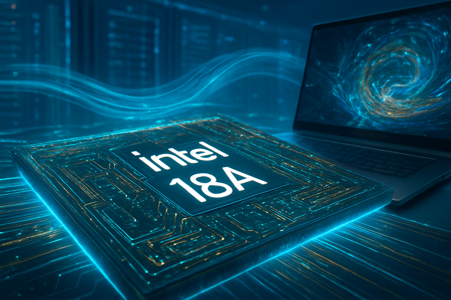
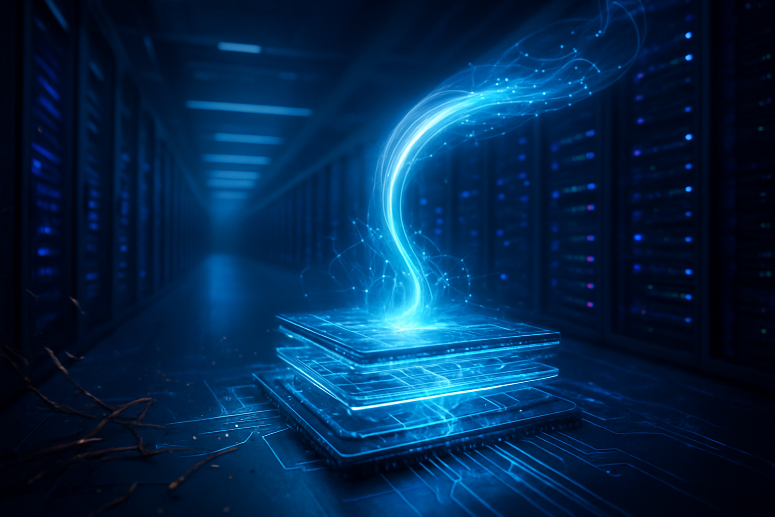
The P&T7 facility is specifically engineered to overcome the daunting physical challenges of HBM4. Unlike its predecessor, HBM3E, which featured a 1024-bit interface, HBM4 doubles the interface width to 2048-bit. This leap allows for staggering bandwidths exceeding 2 TB/s per memory stack. To achieve this, SK Hynix is deploying its proprietary Advanced Mass Reflow Molded Underfill (MR-MUF) technology at P&T7. This process allows the company to stack up to 16 layers of DRAM—offering capacities of 64GB per cube—while keeping the total height within the strict 775-micrometer JEDEC standard. This requires thinning individual DRAM dies to a mere 30 micrometers, a feat of precision engineering that P&T7 is uniquely equipped to handle at scale.
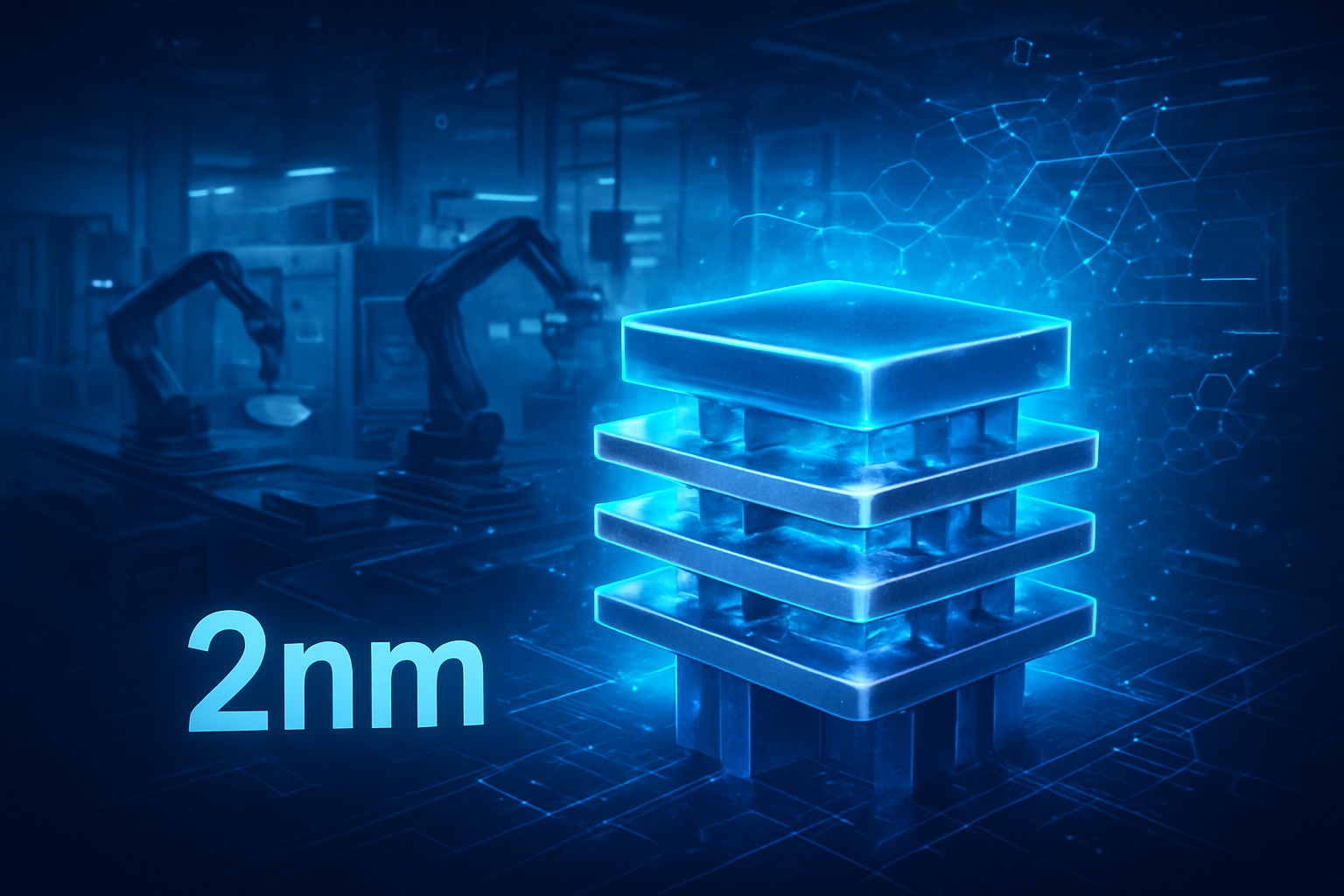
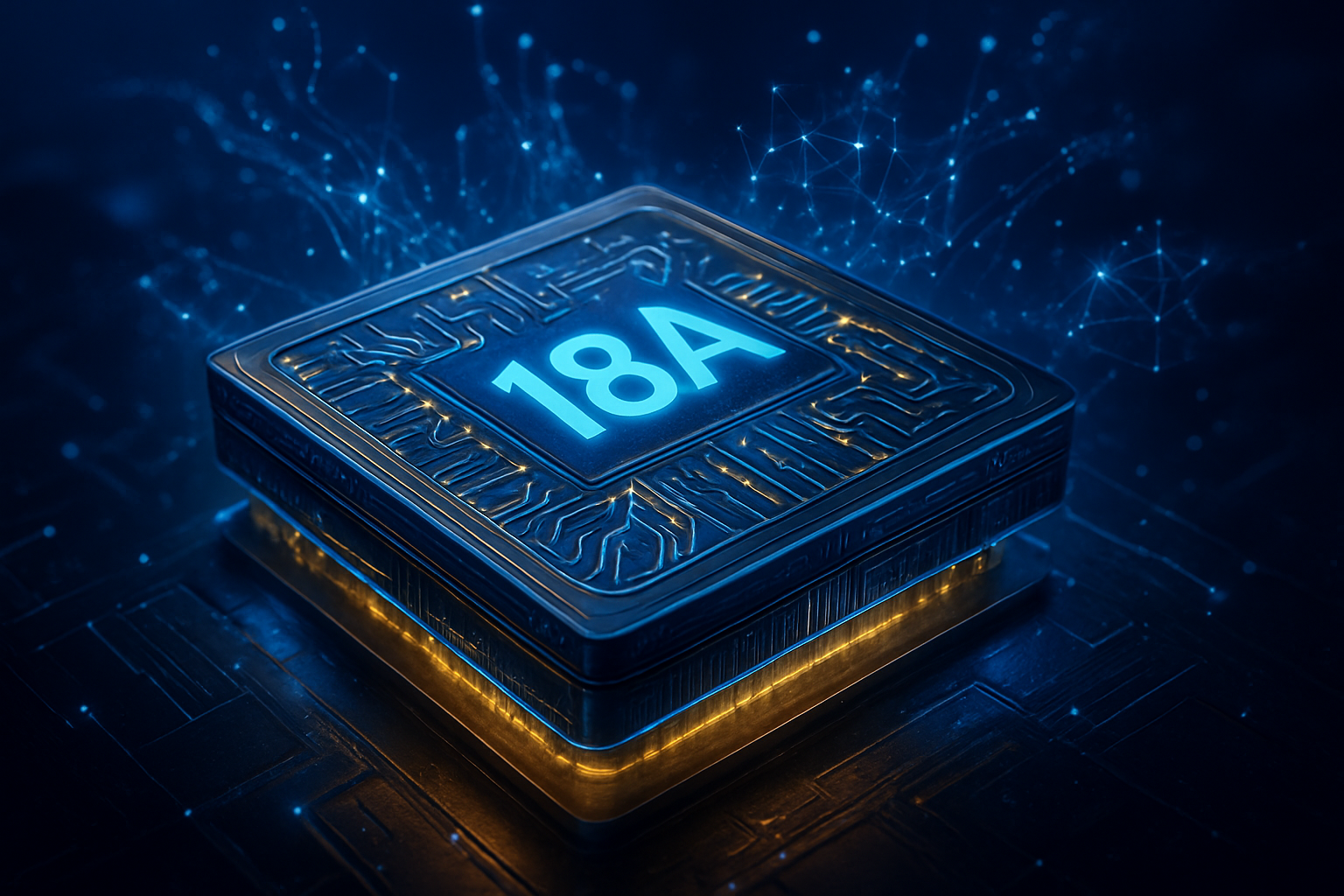
Perhaps the most significant technical shift at P&T7 is the transition of the HBM "base die." In previous generations, the base die was a standard memory component. For HBM4, the base die will be manufactured using advanced logic processes (5nm and 3nm) in collaboration with TSMC (NYSE: TSM). This effectively turns the memory stack into a semi-custom co-processor, allowing for better thermal management and lower latency. The P&T7 plant will act as the final integration point where these TSMC-made logic dies are married to SK Hynix’s high-density DRAM, representing an unprecedented level of cross-foundry collaboration.
Initial reactions from the semiconductor research community suggest that SK Hynix’s decision to stick with MR-MUF for the initial 16-layer HBM4 rollout—rather than jumping immediately to hybrid bonding—is a strategic move to ensure high yields. While competitors are experimenting with hybrid bonding to reduce stack height, SK Hynix’s refined MR-MUF process has already demonstrated superior thermal dissipation, a critical factor for GPUs like NVIDIA’s Blackwell and Rubin that operate at extreme power densities.
Securing the NVIDIA Pipeline: From Blackwell to Rubin
The primary beneficiary of this $13 billion investment is NVIDIA (NASDAQ: NVDA), which has reportedly secured approximately 70% of SK Hynix's HBM4 production capacity through 2027. While SK Hynix currently dominates the supply of HBM3E for the NVIDIA Blackwell (B100/B200) family, the P&T7 facility is built with the future "Rubin" platform in mind. The Rubin GPU is expected to utilize eight stacks of HBM4, providing an astronomical 288GB of ultra-fast memory and 22 TB/s of bandwidth. This leap is essential for the next generation of LLMs, which are expected to exceed 10 trillion parameters.
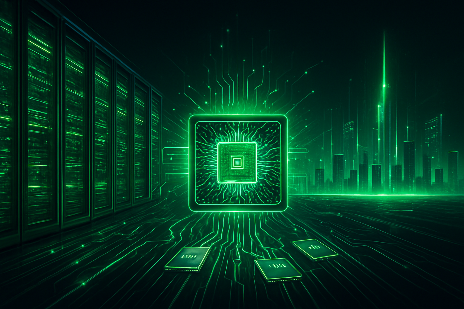
The competitive implications for other tech giants are profound. Samsung (KRX: 005930) and Micron (NASDAQ: MU) are racing to catch up, with Samsung recently passing quality tests for its own HBM4 modules. However, the sheer scale of the P&T7 facility gives SK Hynix a massive advantage in "economies of skill." By housing packaging and testing in such close proximity to the M15X fab, SK Hynix can achieve yield stabilities that are difficult for competitors with fragmented supply chains to match. For hyperscalers like Microsoft (NASDAQ: MSFT) and Meta (NASDAQ: META), who are increasingly designing their own AI silicon, SK Hynix’s P&T7 offers a blueprint for how "custom memory" will be delivered in the late 2020s.
This investment also disrupts the traditional vendor-client relationship. The move toward logic-based base dies means SK Hynix is moving up the value chain, acting more like a boutique foundry for high-performance components rather than a bulk commodity memory supplier. This strategic positioning makes them an indispensable partner for any company attempting to compete at the frontier of AI training and inference.
The Broader AI Landscape: Overcoming the Memory Wall
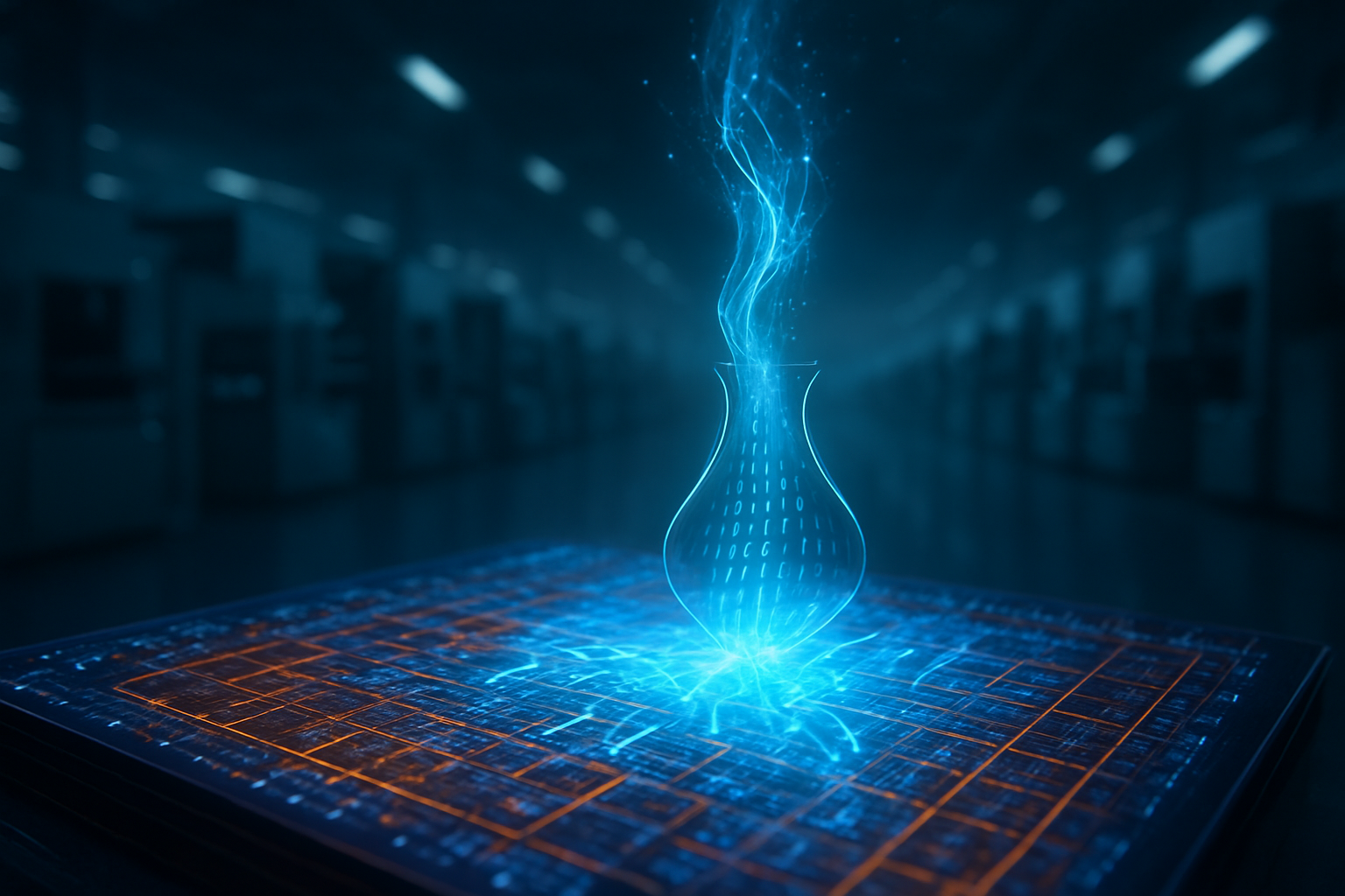
The P&T7 announcement is a direct response to the "Memory Wall"—the growing disparity between how fast a processor can compute and how fast data can be moved into that processor. As AI models grow in complexity, the energy cost of moving data often exceeds the cost of the computation itself. By doubling the bandwidth and increasing the density of HBM4, SK Hynix is effectively extending the lifespan of current transformer-based AI architectures. Without this $13 billion infrastructure, the industry would likely face a hard ceiling on model performance within the next 24 months.
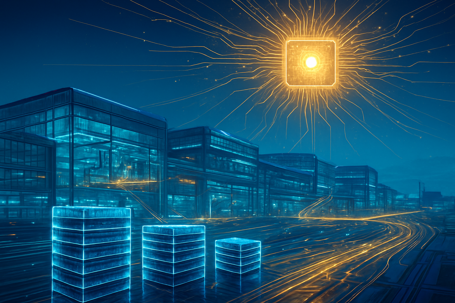
Furthermore, this development highlights the shifting center of gravity in the semiconductor supply chain. While much of the world's focus remains on front-end wafer fabrication in Taiwan, the "back-end" of advanced packaging has become the new bottleneck. SK Hynix’s decision to build the world's largest packaging plant in South Korea—while also expanding into West Lafayette, Indiana—shows a sophisticated "hub-and-spoke" strategy to balance geopolitical security with manufacturing efficiency. It places South Korea at the absolute heart of the AI revolution, making the Cheongju Technopolis as vital to the global economy as any logic fab in Hsinchu.
Comparing this to previous milestones, the P&T7 investment is being viewed by many as the "Gigafactory moment" for the memory industry. Just as massive battery plants were required to make electric vehicles viable, these massive packaging hubs are the prerequisite for the next stage of the AI era. The concern, however, remains one of concentration; with SK Hynix holding such a dominant position in HBM4, any supply chain disruption at the P&T7 site could theoretically stall global AI development for months.
Looking Ahead: The Road to Rubin Ultra and Beyond
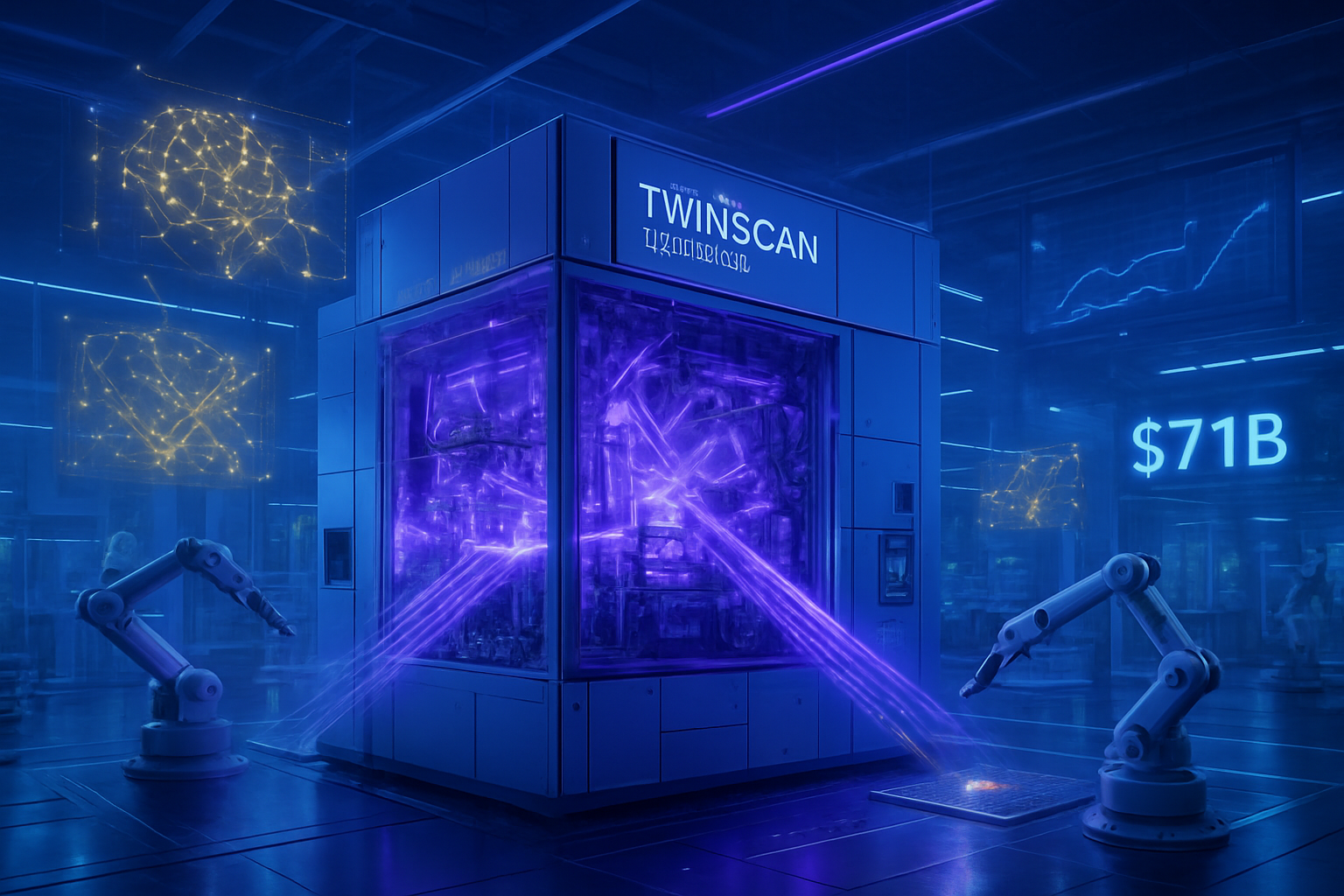
Construction of the P&T7 facility is scheduled to begin in April 2026, with full-scale operations targeted for late 2027. In the near term, SK Hynix will use interim lines and its existing M15X facility to supply the first wave of HBM4 samples to NVIDIA and other tier-one customers. The industry is closely watching for the transition to "Rubin Ultra," a planned refresh of the Rubin architecture that will likely push HBM4 to 20-layer stacks. Experts predict that P&T7 will be the first facility to pilot hybrid bonding at scale for these 20-layer variants, as the physical limits of MR-MUF are eventually reached.
Beyond just GPUs, the high-density memory produced at P&T7 is expected to find its way into high-performance computing (HPC) and even specialized "AI PCs" that require massive local bandwidth for on-device inference. The challenge for SK Hynix will be managing the capital expenditure of such a massive project while the memory market remains notoriously cyclical. However, the "AI-driven" cycle appears to have different dynamics than the traditional PC or smartphone cycles, with demand remaining resilient even in fluctuating economic conditions.
A New Era for AI Hardware
The $13 billion investment in P&T7 is more than just a factory announcement; it is a declaration of dominance. SK Hynix is betting that the future of AI belongs to the company that can most efficiently package and move data. By securing a 70% stake in NVIDIA’s HBM4 orders and building the infrastructure to support the Rubin architecture, SK Hynix has effectively anchored its position as the primary architect of the AI hardware landscape for the remainder of the decade.
Key takeaways from this development include the transition of memory from a commodity to a semi-custom logic-integrated component and the critical role of South Korea as a global hub for advanced packaging. As construction begins this spring, the tech world will be watching P&T7 as the ultimate barometer for the health and velocity of the AI boom. In the coming months, expect to see further announcements regarding the deep integration between SK Hynix, NVIDIA, and TSMC as they finalize the specifications for the first production-ready HBM4 modules.
This content is intended for informational purposes only and represents analysis of current AI developments.
TokenRing AI delivers enterprise-grade solutions for multi-agent AI workflow orchestration, AI-powered development tools, and seamless remote collaboration platforms.
For more information, visit https://www.tokenring.ai/.