San Jose, CA – November 11, 2025 – Navitas Semiconductor (NASDAQ: NVTS), a leading innovator in gallium nitride (GaN) and silicon carbide (SiC) power semiconductors, has embarked on a bold strategic pivot, dubbed "Navitas 2.0," refocusing its efforts squarely on the burgeoning high-power artificial intelligence (AI) markets. This significant reorientation comes on the heels of the company's Q3 2025 financial results, reported on November 3rd, 2025, which saw a considerable stock plunge following disappointing revenue and earnings per share. Despite the immediate market reaction, the company's decisive move towards AI data centers, performance computing, and energy infrastructure positions it as a critical enabler for the next generation of AI, promising a potential long-term recovery and significant impact on the industry.
The "Navitas 2.0" strategy signals a deliberate shift away from lower-margin consumer and mobile segments, particularly in China, towards higher-growth, higher-profit opportunities where its advanced GaN and SiC technologies can provide a distinct competitive advantage. This pivot is a direct response to the escalating power demands of modern AI workloads, which are rapidly outstripping the capabilities of traditional silicon-based power solutions. By concentrating on high-power AI, Navitas aims to capitalize on the foundational need for highly efficient, dense, and reliable power delivery systems that are essential for the "AI factories" of the future.
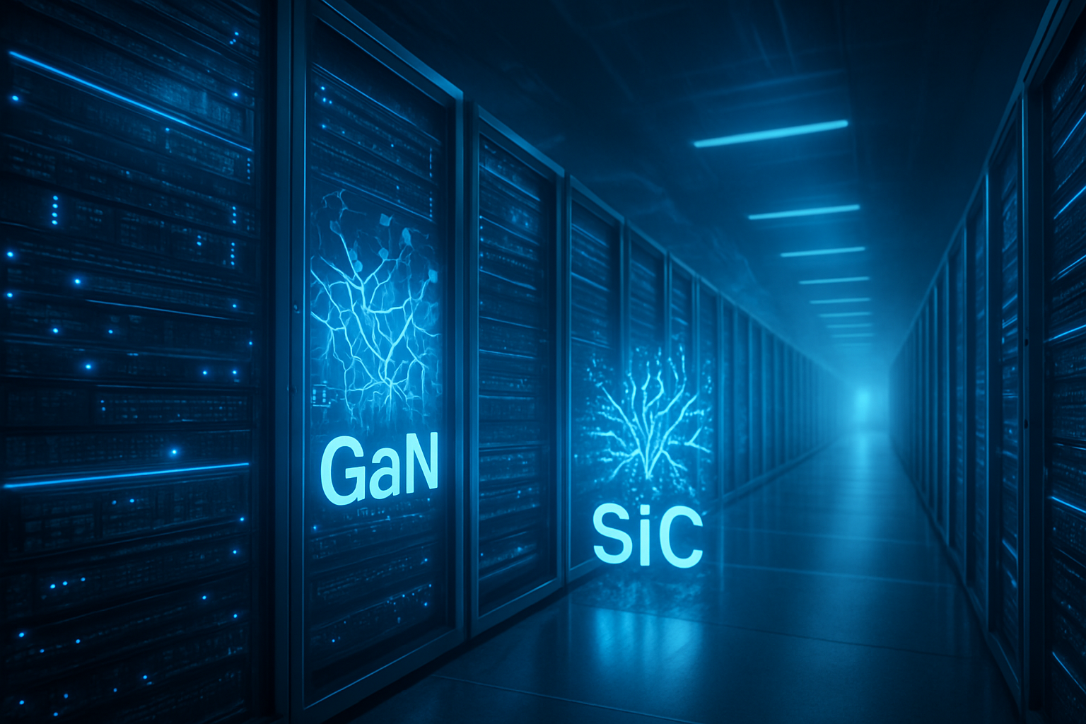
Powering the Future of AI: Navitas's GaN and SiC Technical Edge
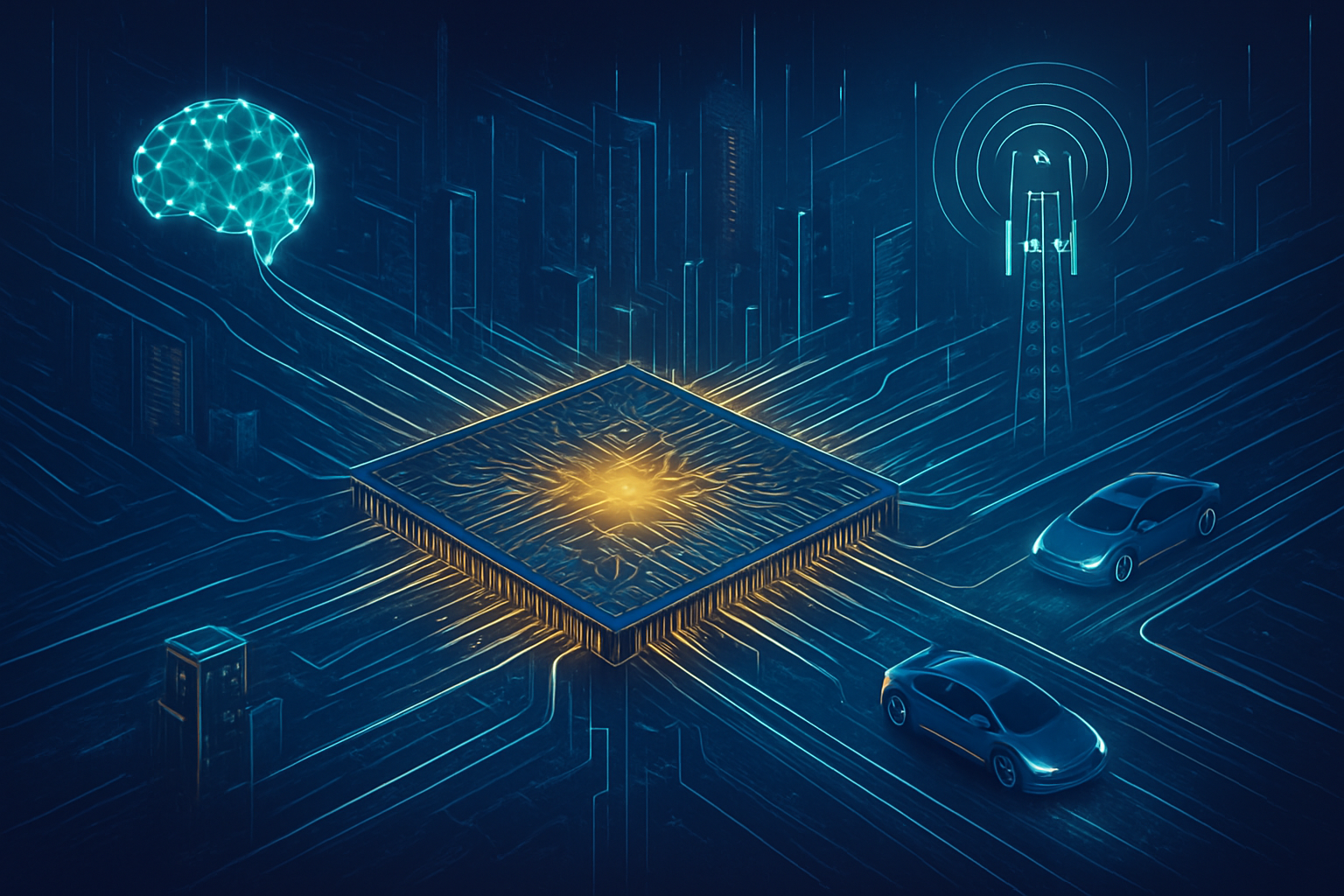
Navitas Semiconductor's strategic pivot is underpinned by its proprietary wide bandgap (WBG) gallium nitride (GaN) and silicon carbide (SiC) technologies. These materials offer a profound leap in performance over traditional silicon in high-power applications, making them indispensable for the stringent requirements of AI data centers, from grid-level power conversion down to the Graphics Processing Unit (GPU).
Navitas's GaN solutions, including its GaNFast™ power ICs, are optimized for high-frequency, high-density DC-DC conversion. These integrated power ICs combine GaN power, drive, control, sensing, and protection, enabling unprecedented power density and energy savings. For instance, Navitas has demonstrated a 4.5 kW, 97%-efficient power supply for AI server racks, achieving a power density of 137 W/in³, significantly surpassing comparable solutions. Their 12 kW GaN and SiC platform boasts an impressive 97.8% peak efficiency. The ability of GaN devices to switch at much higher frequencies allows for smaller, lighter, and more cost-effective passive components, crucial for compact AI infrastructure. Furthermore, the advanced GaNSafe™ ICs integrate critical protection features like short-circuit protection with 350 ns latency and 2 kV ESD protection, ensuring reliability in mission-critical AI environments. Navitas's 100V GaN FET portfolio is specifically tailored for the lower-voltage DC-DC stages on GPU power boards, where thermal management and ultra-high density are paramount.
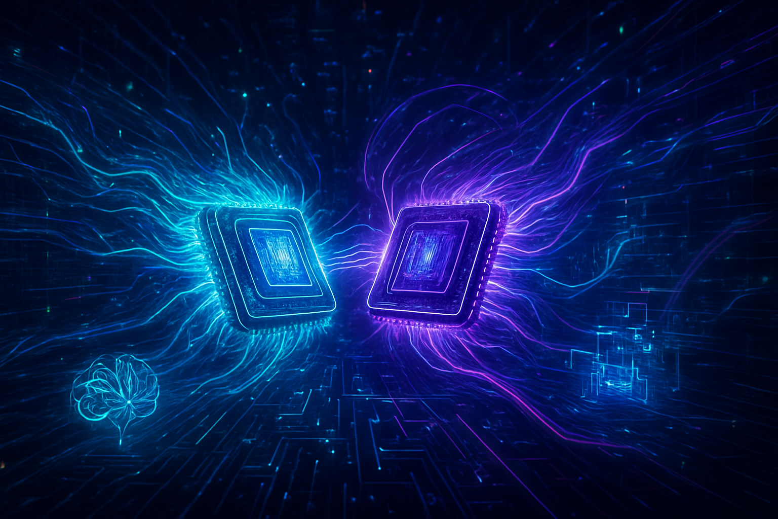
Complementing GaN, Navitas's SiC technologies, under the GeneSiC™ brand, are designed for high-power, high-voltage, and high-reliability applications, particularly in AC grid-to-800 VDC conversion. SiC-based components can withstand higher electric fields, operate at higher voltages and temperatures, and exhibit lower conduction losses, leading to superior efficiency in power conversion. Their Gen-3 Fast SiC MOSFETs, utilizing "trench-assisted planar" technology, are engineered for world-leading performance. Navitas often integrates both GaN and SiC within the same power supply unit, with SiC handling the higher voltage totem-pole Power Factor Correction (PFC) stage and GaN managing the high-frequency LLC stage for optimal performance.
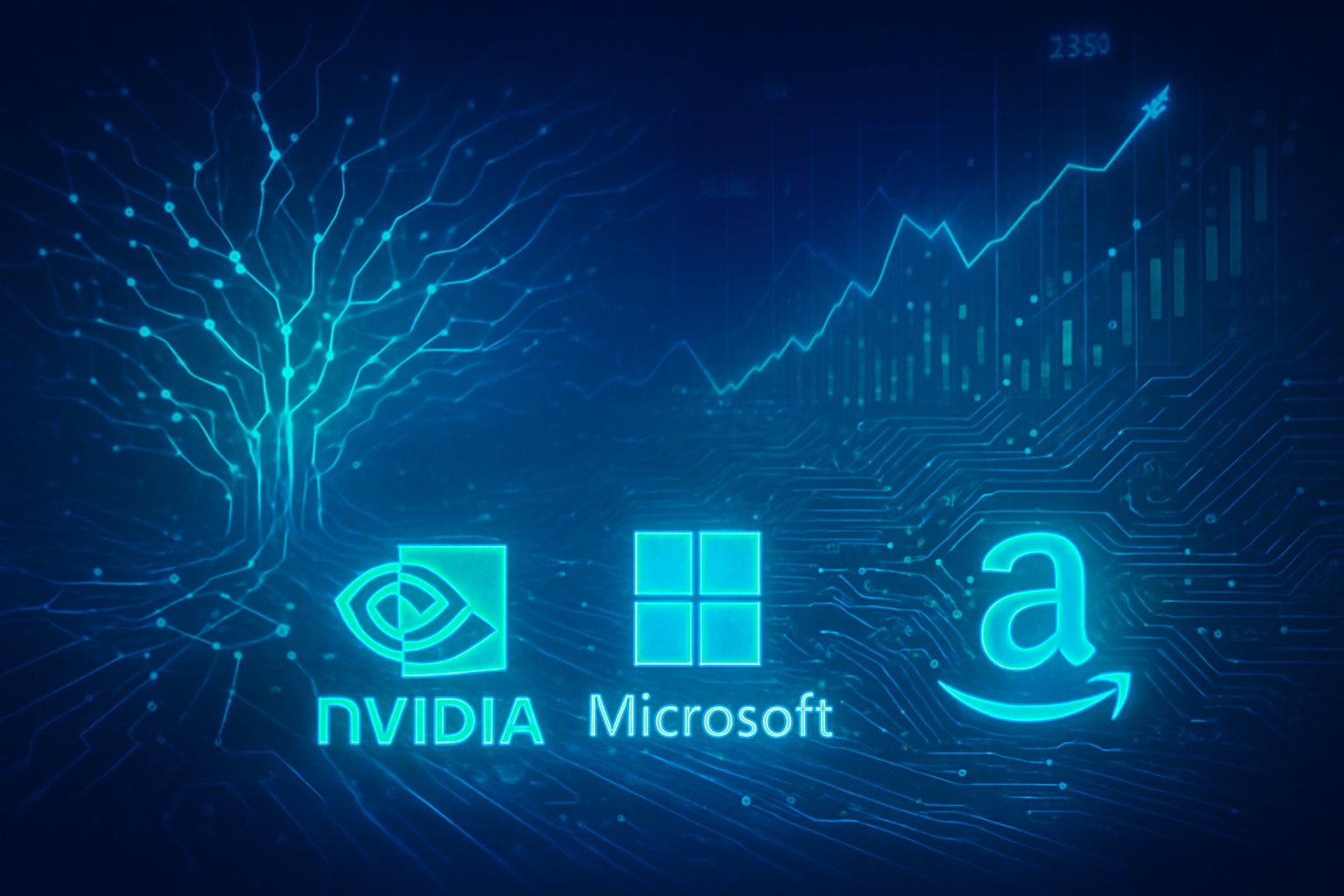
A cornerstone of Navitas's technical strategy is its partnership with NVIDIA (NASDAQ: NVDA), a testament to the efficacy of its WBG solutions. Navitas is supplying advanced GaN and SiC power semiconductors for NVIDIA's next-generation 800V High Voltage Direct Current (HVDC) architecture, central to NVIDIA's "AI factory" computing platforms like "Kyber" rack-scale systems and future GPU solutions. This collaboration is crucial for enabling greater power density, efficiency, reliability, and scalability for the multi-megawatt rack densities demanded by modern AI data centers. Unlike traditional silicon-based approaches that struggle with rising switching losses and limited power density, Navitas's GaN and SiC solutions cut power losses by 50% or more, enabling a fundamental architectural shift to 800V DC systems that reduce copper usage by up to 45% and simplify power distribution.
Reshaping the AI Power Landscape: Industry Implications
Navitas Semiconductor's (NASDAQ: NVTS) strategic pivot to high-power AI markets is poised to significantly reshape the competitive landscape for AI companies, tech giants, and startups alike. The escalating power demands of AI processors necessitate a fundamental shift in power delivery, creating both opportunities and challenges across the industry.
NVIDIA (NASDAQ: NVDA) stands as an immediate and significant beneficiary of Navitas's strategic shift. As a direct partner, NVIDIA relies on Navitas's GaN and SiC solutions to enable its next-generation 800V DC architecture for its AI factory computing. This partnership is critical for NVIDIA to overcome power delivery bottlenecks, allowing for the deployment of increasingly powerful AI processors and maintaining its leadership in the AI hardware space. Other major AI chip developers, such as Intel (NASDAQ: INTC), AMD (NASDAQ: AMD), and Google (NASDAQ: GOOGL), will likely face similar power delivery challenges and will need to adopt comparable high-efficiency, high-density power solutions to remain competitive, potentially seeking partnerships with Navitas or its rivals.
Established power semiconductor manufacturers, including Texas Instruments (NASDAQ: TXN), Infineon (OTC: IFNNY), Wolfspeed (NYSE: WOLF), and ON Semiconductor (NASDAQ: ON), are direct competitors in the high-power GaN/SiC market. Navitas's early mover advantage in AI-specific power solutions and its high-profile partnership with NVIDIA will exert pressure on these players to accelerate their own GaN and SiC developments for AI applications. While these companies have robust offerings, Navitas's integrated solutions and focused roadmap for AI could allow it to capture significant market share. For emerging GaN/SiC startups, Navitas's strong market traction and alliances will intensify competition, requiring them to find niche applications or specialized offerings to differentiate themselves.
The most significant disruption lies in the obsolescence of traditional silicon-based power supply units (PSUs) for advanced AI applications. The performance and efficiency requirements of next-generation AI data centers are exceeding silicon's capabilities. Navitas's solutions, offering superior power density and efficiency, could render legacy silicon-based power supplies uncompetitive, driving a fundamental architectural transformation in data centers. This shift to 800V HVDC reduces energy losses by up to 5% and copper requirements by up to 45%, compelling data centers to adapt their designs, cooling systems, and overall infrastructure. This disruption will also spur the creation of new product categories in power distribution units (PDUs) and uninterruptible power supplies (UPS) optimized for GaN/SiC technology and higher voltages. Navitas's strategic advantages include its technology leadership, early-mover status in AI-specific power, critical partnerships, and a clear product roadmap for increasing power platforms up to 12kW and beyond.
The Broader Canvas: AI's Energy Footprint and Sustainable Innovation
Navitas Semiconductor's (NASDAQ: NVTS) strategic pivot to high-power AI is more than just a corporate restructuring; it's a critical response to one of the most pressing challenges in the broader AI landscape: the escalating energy consumption of artificial intelligence. This shift directly addresses the urgent need for more efficient power delivery as AI's power demands are rapidly becoming a significant bottleneck for further advancement and a major concern for global sustainability.
The proliferation of advanced AI models, particularly large language models and generative AI, requires immense computational power, translating into unprecedented electricity consumption. Projections indicate that AI's energy demand could account for 27-50% of total data center energy consumption by 2030, a dramatic increase from current levels. High-performance AI processors now consume hundreds of watts each, with future generations expected to exceed 1000W, pushing server rack power requirements from a few kilowatts to over 100 kW. Navitas's focus on high-power, high-density, and highly efficient GaN and SiC solutions is therefore not merely an improvement but an enabler for managing this exponential growth without proportionate increases in physical footprint and operational costs. Their 4.5kW platforms, combining GaN and SiC, achieve power densities over 130W/in³ and efficiencies over 97%, demonstrating a path to sustainable AI scaling.
The environmental impact of this pivot is substantial. The increasing energy consumption of AI poses significant sustainability challenges, with data centers projected to more than double their electricity demand by 2030. Navitas's wide-bandgap semiconductors inherently reduce energy waste, minimize heat generation, and decrease the overall material footprint of power systems. Navitas estimates that each GaN power IC shipped reduces CO2 emissions by over 4 kg compared to legacy silicon chips, and SiC MOSFETs save over 25 kg of CO2. The company projects that widespread adoption of GaN and SiC could lead to a reduction of approximately 6 Gtons of CO2 per year by 2050, equivalent to the CO2 generated by over 650 coal-fired power stations. These efficiencies are crucial for achieving global net-zero carbon ambitions and translate into lower operational costs for data centers, making sustainable practices economically viable.
However, this strategic shift is not without its concerns. The transition away from established mobile and consumer markets is expected to cause short-term revenue depression for Navitas, introducing execution risks as the company realigns resources and accelerates product roadmaps. Analysts have raised questions about sustainable cash burn and the intense competitive landscape. Broader concerns include the potential strain on existing electricity grids due to the "always-on" nature of AI operations and potential manufacturing capacity constraints for GaN, especially with concentrated production in Taiwan. Geopolitical factors affecting the semiconductor supply chain also pose risks.
In comparison to previous AI milestones, Navitas's contribution is a hardware-centric breakthrough in power delivery, distinct from, yet equally vital as, advancements in processing power or data storage. Historically, computing milestones focused on miniaturization and increasing transistor density (Moore's Law) to boost computational speed. While these led to significant performance gains, power efficiency often lagged. The development of specialized accelerators like GPUs dramatically improved the efficiency of AI workloads, but the "power problem" persisted. Navitas's innovation addresses this fundamental power infrastructure, enabling the architectural changes (like 800V DC systems) necessary to support the "AI revolution." Without such power delivery breakthroughs, the energy footprint of AI could become economically and environmentally unsustainable, limiting its potential. This pivot ensures that the processing power of AI can be effectively and sustainably delivered, unlocking the full potential of future AI breakthroughs.
The Road Ahead: Future Developments and Expert Outlook
Navitas Semiconductor's (NASDAQ: NVTS) strategic pivot to high-power AI marks a critical juncture, setting the stage for significant near-term and long-term developments not only for the company but for the entire AI industry. The "Navitas 2.0" transformation is a bold bet on the future, driven by the insatiable power demands of next-generation AI.
In the near term, Navitas is intensely focused on accelerating its AI power roadmap. This includes deepening its collaboration with NVIDIA (NASDAQ: NVDA), providing advanced GaN and SiC power semiconductors for NVIDIA's 800V DC architecture in AI factory computing. The company has already made substantial progress, releasing the world's first 8.5 kW AI data center power supply unit (PSU) with 98% efficiency and a 12 kW PSU for hyperscale AI data centers achieving 97.8% peak efficiency, both leveraging GaN and SiC and complying with Open Compute Project (OCP) and Open Rack v3 (ORv3) specifications. Further product introductions include a portfolio of 100V and 650V discrete GaNFast™ FETs, GaNSafe™ ICs with integrated protection, and high-voltage SiC products. The upcoming release of 650V bidirectional GaN switches and the continued refinement of digital control techniques like IntelliWeave™ promise even greater efficiency and reliability. Navitas anticipates that Q4 2025 will represent a revenue bottom, with sequential growth expected to resume in 2026 as its strategic shift gains traction.
Looking further ahead, Navitas's long-term vision is to solidify its leadership in high-power markets, delivering enhanced business scale and quality. This involves continually advancing its AI power roadmap, aiming for PSUs with power levels exceeding 12kW. The partnership with NVIDIA is expected to evolve, leading to more specialized GaN and SiC solutions for future AI accelerators and modular data center power architectures. With a strong balance sheet and substantial cash reserves, Navitas is well-positioned to fund the capital-intensive R&D and manufacturing required for these ambitious projects.
The broader high-power AI market is projected for explosive growth, with the global AI data center market expected to reach nearly $934 billion by 2030, driven by the demand for smaller, faster, and more energy-efficient semiconductors. This market is undergoing a fundamental shift towards newer power architectures like 800V HVDC, essential for the multi-megawatt rack densities of "AI factories." Beyond data centers, Navitas's advanced GaN and SiC technologies are critical for performance computing, energy infrastructure (solar inverters, energy storage), industrial electrification (motor drives, robotics), and even edge AI applications, where high performance and minimal power consumption are crucial.
Despite the promising outlook, significant challenges remain. The extreme power consumption of AI chips (700-1200W per chip) necessitates advanced cooling solutions and energy-efficient designs to prevent localized hot spots. High current densities and miniaturization also pose challenges for reliable power delivery. For Navitas specifically, the transition from mobile to high-power markets involves an extended go-to-market timeline and intense competition, requiring careful execution to overcome short-term revenue dips. Manufacturing capacity constraints for GaN, particularly with concentrated production in Taiwan, and supply chain vulnerabilities also present risks.
Experts generally agree that Navitas is well-positioned to maintain a leading role in the GaN power device market due to its integrated solutions and diverse application portfolio. The convergence of AI, electrification, and sustainable energy is seen as the primary accelerator for GaN technology. However, investors remain cautious, demanding tangible design wins and clear pathways to near-term profitability. The period of late 2025 and early 2026 is viewed as a critical transition phase for Navitas, where the success of its strategic pivot will become more evident. Continued innovation in GaN and SiC, coupled with a focus on sustainability and addressing the unique power challenges of AI, will be key to Navitas's long-term success and its role in enabling the next era of artificial intelligence.
Comprehensive Wrap-Up: A Pivotal Moment for AI Power
Navitas Semiconductor's (NASDAQ: NVTS) "Navitas 2.0" strategic pivot marks a truly pivotal moment in the company's trajectory and, more broadly, in the evolution of AI infrastructure. The decision to shift from lower-margin consumer electronics to the demanding, high-growth arena of high-power AI, driven by advanced GaN and SiC technologies, is a bold, necessary, and potentially transformative move. While the immediate aftermath of its Q3 2025 results saw a stock plunge, reflecting investor apprehension about short-term financial performance, the long-term implications position Navitas as a critical enabler for the future of artificial intelligence.
The key takeaway is that the scaling of AI is now inextricably linked to advancements in power delivery. Traditional silicon-based solutions are simply insufficient for the multi-megawatt rack densities and unprecedented power demands of modern AI data centers. Navitas, with its superior GaN and SiC wide bandgap semiconductors, offers a compelling solution: higher efficiency, greater power density, and enhanced reliability. Its partnership with NVIDIA (NASDAQ: NVDA) for 800V DC "AI factory" architectures is a strong validation of its technological leadership and strategic foresight. This shift is not just about incremental improvements; it's about enabling a fundamental architectural transformation in how AI is powered, reducing energy waste, and fostering sustainability.
In the grand narrative of AI history, this development aligns with previous hardware breakthroughs that unlocked new computational capabilities. Just as specialized processors like GPUs accelerated AI training, advancements in efficient power delivery are now crucial to sustain and scale these powerful systems. Without companies like Navitas addressing the "power problem," the energy footprint of AI could become economically and environmentally unsustainable, limiting its potential. This pivot signifies a recognition that the physical infrastructure underpinning AI is as critical as the algorithms and processing units themselves.
In the coming weeks and months, all eyes will be on Navitas's execution of its "Navitas 2.0" strategy. Investors and industry observers will be watching for tangible design wins, further product deployments in AI data centers, and clear signs of revenue growth in its new target markets. The pace at which Navitas can transition its business, manage competitive pressures from established players, and navigate potential supply chain challenges will determine the ultimate success of this ambitious repositioning. If successful, Navitas Semiconductor could emerge not just as a survivor of its post-Q3 downturn, but as a foundational pillar in the sustainable development and expansion of the global AI ecosystem.
This content is intended for informational purposes only and represents analysis of current AI developments.
TokenRing AI delivers enterprise-grade solutions for multi-agent AI workflow orchestration, AI-powered development tools, and seamless remote collaboration platforms.
For more information, visit https://www.tokenring.ai/.