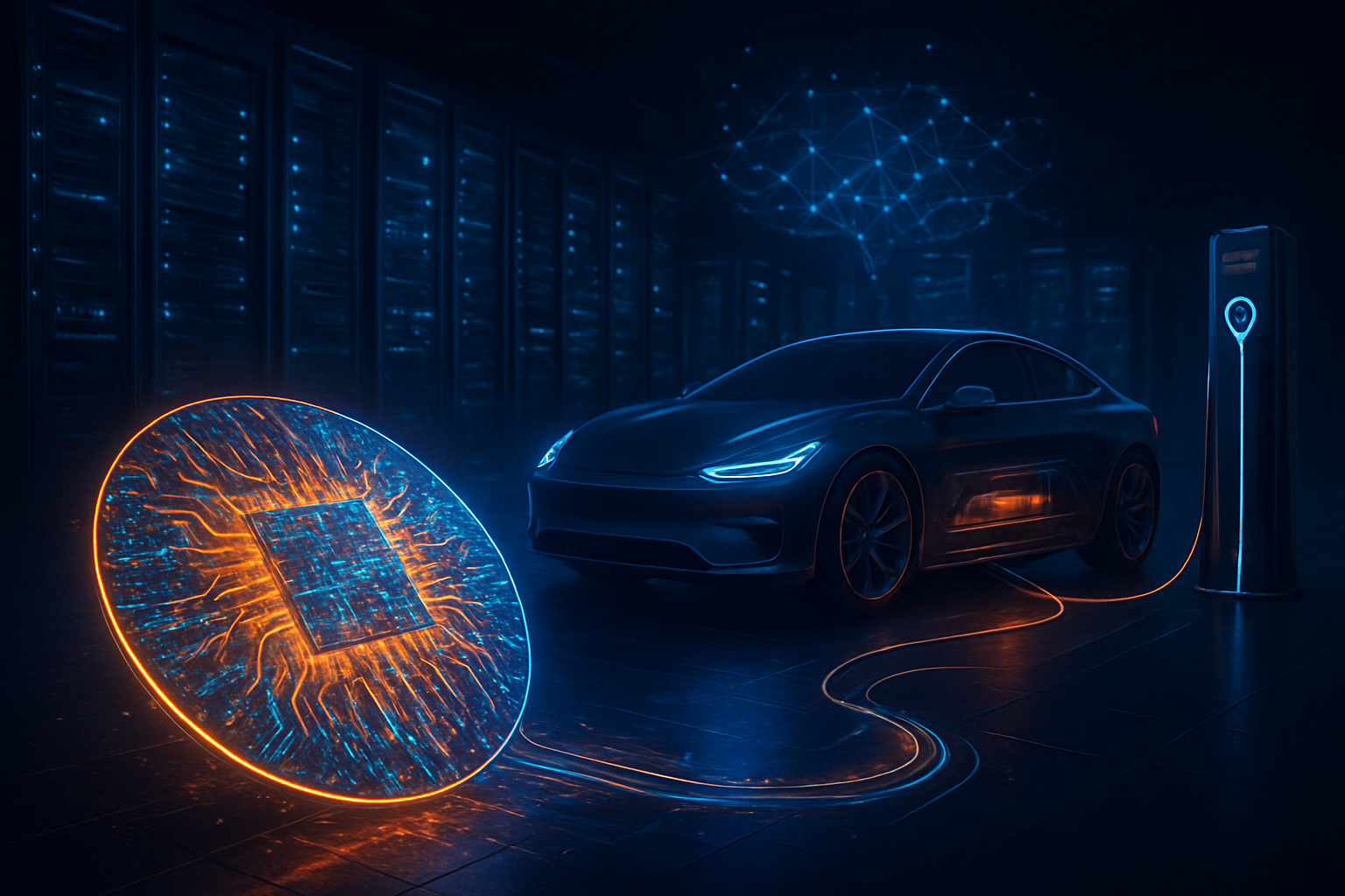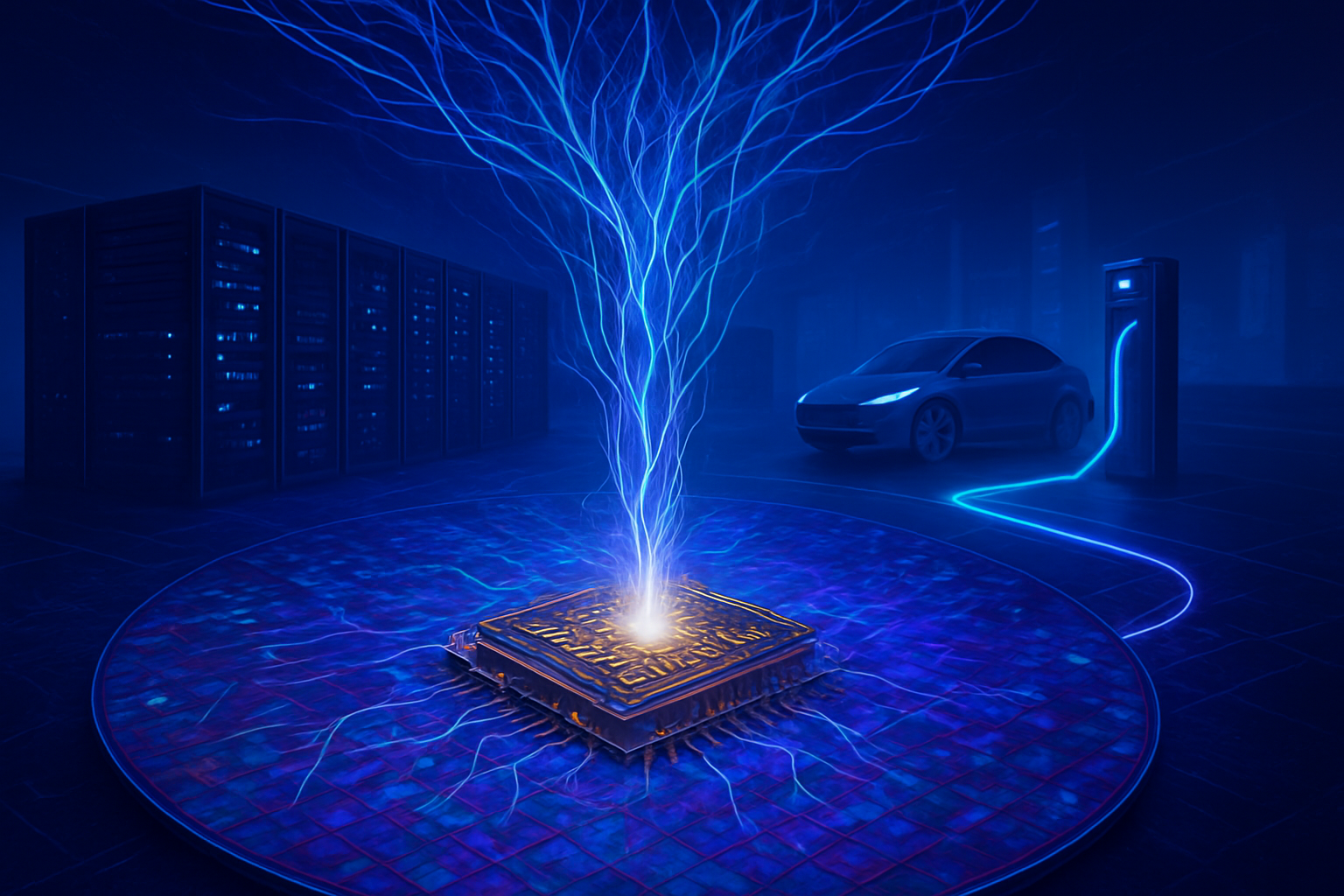
The global technology landscape is currently undergoing its most significant hardware transformation since the invention of the silicon transistor. As of January 21, 2026, the transition from traditional silicon to Wide-Bandgap (WBG) semiconductors—specifically Gallium Nitride (GaN) and Silicon Carbide (SiC)—has reached a fever pitch. This "Power Revolution" is no longer a niche upgrade; it has become the fundamental backbone of the artificial intelligence boom and the mass adoption of 800V electric vehicle (EV) architectures. Without these advanced materials, the massive power demands of next-generation AI data centers and the range requirements of modern EVs would be virtually impossible to sustain.
The immediate significance of this shift is measurable in raw efficiency and physical scale. In the first few weeks of 2026, we have seen the industry move from 200mm (8-inch) production standards to the long-awaited 300mm (12-inch) wafer milestone. This evolution is slashing the cost of high-performance power chips, bringing them toward price parity with silicon while delivering up to 99% system efficiency. As AI chips like NVIDIA’s latest "Rubin" architecture push past the 1,000-watt-per-chip threshold, the ability of GaN and SiC to handle extreme heat and high voltages in a fraction of the space is the only factor preventing a total energy grid crisis.
Technical Milestones: Breaking the Silicon Ceiling
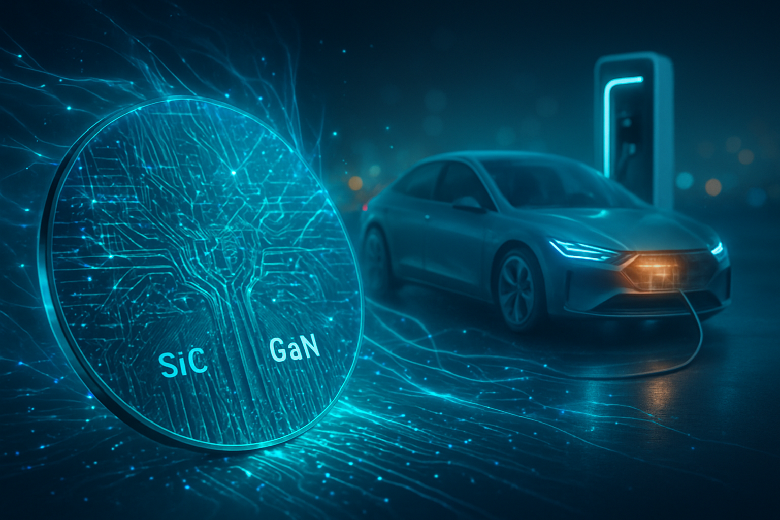
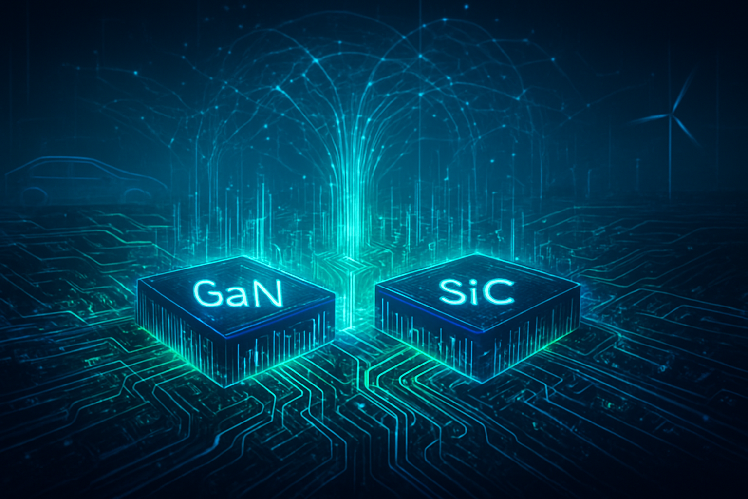
The technical superiority of WBG semiconductors stems from their ability to operate at much higher voltages, temperatures, and frequencies than traditional silicon. Silicon Carbide (SiC) has established itself as the "muscle" for high-voltage traction in EVs, while Gallium Nitride (GaN) has emerged as the high-speed engine for data center power supplies. A major breakthrough announced in early January 2026 involves the widespread commercialization of Vertical GaN architecture. Unlike traditional lateral GaN, vertical structures allow devices to operate at 1200V and above, enabling a 30% increase in efficiency and a 50% reduction in the physical footprint of power supply units (PSUs).
In the data center, these advancements have manifested in the move toward 800V High-Voltage Direct Current (HVDC) power stacks. By switching from AC to 800V DC, data center operators are minimizing conversion losses that previously plagued large-scale AI clusters. Modern GaN-based PSUs are now achieving record-breaking 97.5% peak efficiency, allowing a standard server rack to quadruple its power density. Where a legacy 3kW module once sat, engineers can now fit a 12kW unit in the same physical space. This miniaturization is further supported by "wire-bondless" packaging and silver sintering techniques that replace old-fashioned copper wiring with high-performance thermal interfaces.
Initial reactions from the semiconductor research community have been overwhelmingly positive, with experts noting that the transition to 300mm single-crystal SiC wafers—first demonstrated by Wolfspeed early this month—is a "Moore's Law moment" for power electronics. The ability to produce 2.3 times more chips per wafer is expected to drive down costs by nearly 40% over the next 18 months. This technical leap effectively ends the era of silicon dominance in power applications, as the performance-to-cost ratio finally tips in favor of WBG materials.
Market Impact: The New Power Players
The shift to WBG semiconductors has sparked a massive realignment among chipmakers and tech giants. Wolfspeed (NYSE: WOLF), having successfully navigated a strategic restructuring in late 2025, has emerged as a vertically integrated leader in 200mm and 300mm SiC production. Their ability to control the supply chain from raw crystal growth to finished chips has given them a significant edge in the EV market. Similarly, STMicroelectronics (NYSE: STM) has ramped up production at its Catania campus to 15,000 wafers per week, securing its position as a primary supplier for European and American automakers.
Other major beneficiaries include Infineon Technologies (OTC: IFNNY) and ON Semiconductor (NASDAQ: ON), both of whom have forged deep collaborations with NVIDIA (NASDAQ: NVDA). As AI "factories" require unprecedented amounts of electricity, NVIDIA has integrated these WBG-enabled power stacks directly into its reference designs. This "Grid-to-Processor" strategy ensures that the power delivery is as efficient as the computation itself. Startups in the GaN space, such as Navitas Semiconductor, are also seeing increased valuation as they disrupt the consumer electronics and onboard charger (OBC) markets with ultra-compact, high-speed switching solutions.
This development is creating a strategic disadvantage for companies that have been slow to pivot away from silicon-based Insulated Gate Bipolar Transistors (IGBTs). While legacy silicon still holds the low-end consumer market, the high-margin sectors of AI and EVs are now firmly WBG-territory. Major tech companies are increasingly viewing power efficiency as a competitive "moat"—if a data center can run 20% more AI chips on the same power budget because of SiC and GaN, that company gains a massive lead in the ongoing AI arms race.
Broader Significance: Sustaining the AI Boom
The wider significance of the WBG revolution cannot be overstated; it is the "green" solution to a brown-energy problem. The AI industry has faced intense scrutiny over its massive electricity consumption, but the deployment of WBG semiconductors offers a tangible way to mitigate environmental impact. By reducing power conversion losses, these materials could save hundreds of terawatt-hours of electricity globally by the end of the decade. This aligns with the aggressive ESG (Environmental, Social, and Governance) targets set by tech giants who are struggling to balance their AI ambitions with carbon-neutrality goals.
Historically, this transition is being compared to the shift from vacuum tubes to transistors. While the transistor allowed for the miniaturization of logic, WBG materials are allowing for the miniaturization and "greening" of power. However, concerns remain regarding the supply of raw materials like high-purity carbon and gallium, as well as the geopolitical tensions surrounding the semiconductor supply chain. Ensuring a stable supply of these "power minerals" is now a matter of national security for major economies.
Furthermore, the impact on the EV industry is transformative. By making 800V architectures the standard, the "range anxiety" that has plagued EV adoption is rapidly disappearing. With SiC-enabled 500kW chargers, vehicles can now add 400km of range in just five minutes—the same time it takes to fill a gas tank. This parity with internal combustion engines is the final hurdle for mass-market EV transition, and it is being cleared by the physical properties of Silicon Carbide.
The Horizon: From 1200V to Gallium Oxide
Looking toward the near-term future, we expect the vertical GaN market to mature, potentially displacing SiC in certain mid-voltage EV applications. Researchers are also beginning to look beyond SiC and GaN toward Gallium Oxide (Ga2O3), an Ultra-Wide-Bandgap (UWBG) material that promises even higher breakdown voltages and lower losses. While Ga2O3 is still in the experimental phase, early prototypes suggest it could be the key to 3000V+ industrial power systems and future-generation electric aviation.
In the long term, we anticipate a complete "power integration" where the power supply is no longer a separate brick but is integrated directly onto the same package as the processor. This "Power-on-Chip" concept, enabled by the high-frequency capabilities of GaN, could eliminate even more efficiency losses and lead to even smaller, more powerful AI devices. The primary challenge remains the cost of manufacturing and the complexity of thermal management at such extreme power densities, but experts predict that the 300mm wafer transition will solve the economics of this problem by 2027.
Conclusion: A New Era of Efficiency
The revolution in Wide-Bandgap semiconductors represents a fundamental shift in how the world manages and consumes energy. From the high-voltage demands of a Tesla or BYD to the massive computational clusters of an NVIDIA AI factory, GaN and SiC are the invisible heroes of the modern tech era. The milestones achieved in early 2026—specifically the transition to 300mm wafers and the rise of 800V HVDC data centers—mark the point of no return for traditional silicon in high-performance power applications.
As we look ahead, the significance of this development in AI history will be seen as the moment hardware efficiency finally began to catch up with algorithmic demand. The "Power Revolution" has provided a lifeline to an industry that was beginning to hit a physical wall. In the coming weeks and months, watch for more automotive OEMs to announce the phase-out of 400V systems in favor of WBG-powered 800V platforms, and for data center operators to report significant energy savings as they upgrade to these next-generation power stacks.
This content is intended for informational purposes only and represents analysis of current AI and semiconductor developments.
TokenRing AI delivers enterprise-grade solutions for multi-agent AI workflow orchestration, AI-powered development tools, and seamless remote collaboration platforms.
For more information, visit https://www.tokenring.ai/.