Tag: SiC

  • The Wide-Bandgap Revolution: GaN and SiC Power Devices Reshape the Future of Electronics

    The Wide-Bandgap Revolution: GaN and SiC Power Devices Reshape the Future of Electronics

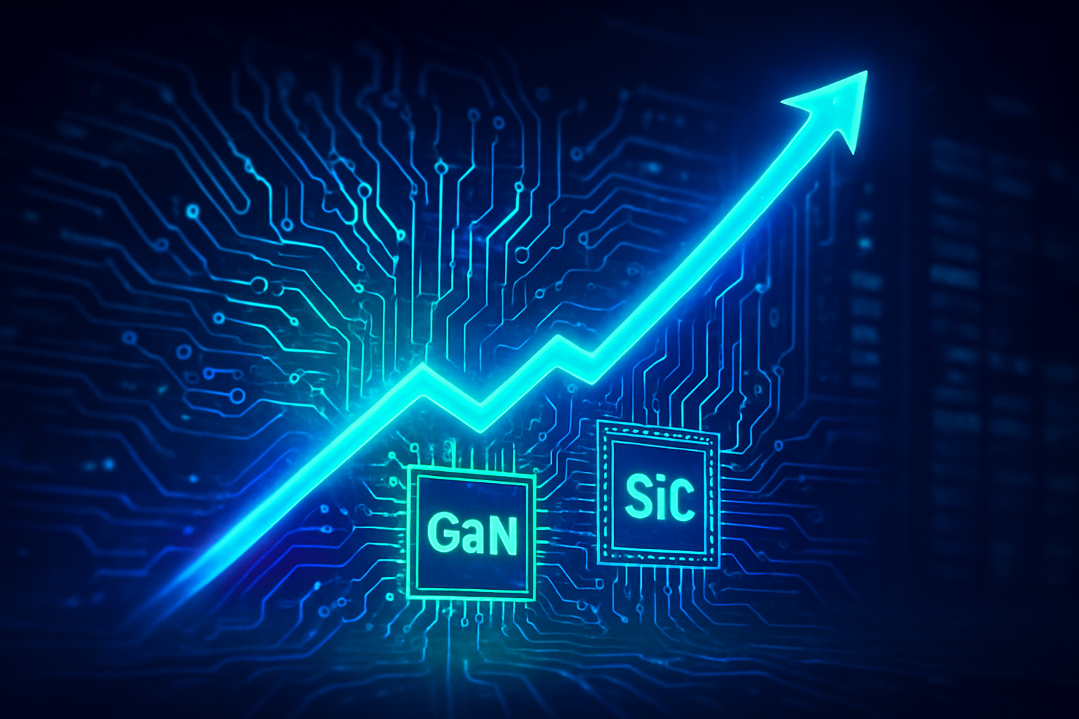
    The semiconductor industry is on the cusp of a profound transformation, driven by the escalating adoption and strategic alliances surrounding next-generation power devices built with Gallium Nitride (GaN) and Silicon Carbide (SiC). These wide-bandgap (WBG) materials are rapidly displacing traditional silicon in high-performance applications, promising unprecedented levels of efficiency, power density, and thermal management. As of December 2025, the convergence of advanced manufacturing techniques, significant cost reductions, and a surge in demand from critical sectors like electric vehicles (EVs), AI data centers, and renewable energy is cementing GaN and SiC's role as foundational technologies for the coming decades.

    This paradigm shift is not merely an incremental improvement; it represents a fundamental rethinking of power electronics design. With their superior inherent properties, GaN and SiC enable devices that can switch faster, operate at higher temperatures, and handle greater power with significantly less energy loss than their silicon counterparts. This immediate significance translates into smaller, lighter, and more energy-efficient systems across a vast array of applications, propelling innovation and addressing pressing global challenges related to energy consumption and sustainability.

    Unpacking the Technical Edge: How GaN and SiC Redefine Power

    The technical advancements in GaN and SiC power devices are multifaceted, focusing on optimizing their intrinsic material properties to push the boundaries of power conversion. Unlike silicon, GaN and SiC possess a wider bandgap, higher electron mobility, and superior thermal conductivity. These characteristics allow them to operate at much higher voltages, frequencies, and temperatures without compromising efficiency or reliability.

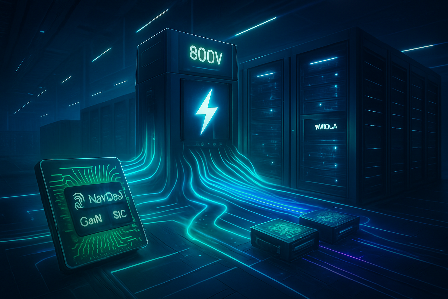
    Recent breakthroughs include the mass production of 300mm GaN wafers, a critical step towards cost reduction and broader market penetration in high-power consumer and automotive applications. Similarly, the transition to 8-inch SiC wafers is improving yields and lowering per-device costs. In device architecture, innovations like monolithic bidirectional GaN switches are enabling highly efficient EV onboard chargers that are up to 40% smaller and achieve over 97.5% efficiency. New generations of 1200V SiC MOSFETs boast up to 30% lower switching losses, directly impacting the performance of EV traction inverters and industrial drives. Furthermore, hybrid GaN/SiC integration is supporting ultra-high-voltage and high-frequency power conversion vital for cutting-edge AI data centers and 800V EV drivetrains.

    These advancements fundamentally differ from previous silicon-based approaches by offering a step-change in performance. Silicon's physical limits for high-frequency and high-power applications have been largely reached. GaN and SiC, by contrast, offer lower conduction and switching losses, higher power density, and better thermal performance, which translates directly into smaller form factors, reduced cooling requirements, and significantly higher energy efficiency. The initial reaction from the AI research community and industry experts has been overwhelmingly positive, with many recognizing these materials as essential enablers for next-generation computing and energy infrastructure. The ability to manage power more efficiently at higher frequencies is particularly crucial for AI accelerators and data centers, where power consumption and heat dissipation are enormous challenges.

    Corporate Chessboard: Companies Vying for Wide-Bandgap Dominance

    The rise of GaN and SiC has ignited a fierce competitive landscape and fostered a wave of strategic alliances among semiconductor giants, tech titans, and innovative startups. Companies like Infineon Technologies AG (ETR: IFX), STMicroelectronics (NYSE: STM), Wolfspeed (NYSE: WOLF), ROHM Semiconductor (TYO: 6767), onsemi (NASDAQ: ON), and Navitas Semiconductor (NASDAQ: NVTS) are at the forefront, investing heavily in R&D, manufacturing capacity, and market development.

    These companies stand to benefit immensely from the growing adoption of WBG materials. For instance, Infineon Technologies AG (ETR: IFX) is pioneering 300mm GaN wafers and expanding its SiC production to meet surging demand, particularly from the automotive sector. GlobalFoundries (NASDAQ: GFS) and Navitas Semiconductor (NASDAQ: NVTS) have formed a long-term strategic alliance to bolster U.S.-focused GaN technology and manufacturing for critical high-power applications. Similarly, onsemi (NASDAQ: ON) and Innoscience have entered a deep cooperation to jointly develop high-efficiency GaN power devices, leveraging Innoscience's 8-inch silicon-based GaN process platform. These alliances are crucial for accelerating innovation, scaling production, and securing supply chains in a rapidly expanding market.

    The competitive implications for major AI labs and tech companies are significant. As AI workloads demand ever-increasing computational power, the energy efficiency offered by GaN and SiC in power supply units (PSUs) becomes critical. Companies like NVIDIA Corporation (NASDAQ: NVDA), heavily invested in AI infrastructure, are already partnering with GaN leaders like Innoscience for their 800V DC power supply architectures for AI data centers. This development has the potential to disrupt existing power management solutions, making traditional silicon-based PSUs less competitive in terms of efficiency and form factor. Companies that successfully integrate GaN and SiC into their products will gain a strategic advantage through superior performance, smaller footprints, and reduced operating costs for their customers.

    A Broader Horizon: Impact on AI, Energy, and Global Trends

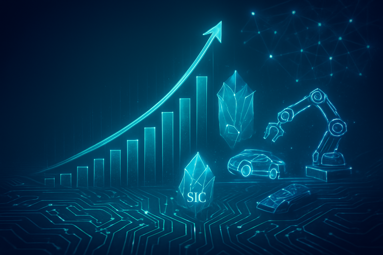
    The widespread adoption of GaN and SiC power devices extends far beyond individual company balance sheets, fitting seamlessly into broader AI, energy, and global technological trends. These materials are indispensable enablers for the global transition towards a more energy-efficient and sustainable future. Their ability to minimize energy losses is directly contributing to carbon neutrality goals, particularly in energy-intensive sectors.

    In the context of AI, the impact is profound. AI data centers are notorious for their massive energy consumption and heat generation. GaN and SiC-based power supplies and converters dramatically improve the efficiency of power delivery within these centers, reducing rack power loss and cutting facility energy costs. This allows for denser server racks and more powerful AI accelerators, pushing the boundaries of what is computationally feasible. Beyond data centers, these materials are crucial for the rapid expansion of electric vehicles, enabling faster charging, longer ranges, and more compact power electronics. They are also integral to renewable energy systems, enhancing the efficiency of solar inverters, wind turbines, and energy storage solutions, thereby facilitating better grid integration and management.

    Potential concerns, however, include the initial higher cost compared to silicon, the need for specialized manufacturing facilities, and the complexity of designing with these high-frequency devices (e.g., managing EMI and parasitic inductance). Nevertheless, the industry is actively addressing these challenges, with costs reaching near-parity with silicon in 2025 for many applications, and design tools becoming more sophisticated. This shift can be compared to previous semiconductor milestones, such as the transition from germanium to silicon, marking a similar fundamental leap in material science that unlocked new levels of performance and application possibilities.

    The Road Ahead: Charting Future Developments and Applications

    The trajectory for GaN and SiC power devices points towards continued innovation and expanding applications. In the near term, experts predict further advancements in packaging technologies, leading to more integrated power modules that simplify design and improve thermal performance. The development of higher voltage GaN devices, potentially challenging SiC in some 900-1200V segments, is also on the horizon, with research into vertical GaN and new material platforms like GaN-on-Sapphire gaining momentum.

    Looking further out, the potential applications and use cases are vast. Beyond current applications in EVs, data centers, and consumer electronics, GaN and SiC are expected to play a critical role in advanced robotics, aerospace power systems, smart grids, and even medical devices where miniaturization and efficiency are paramount. The continuous drive for higher power density and efficiency will push these materials into new frontiers, enabling devices that are currently impractical with silicon.

    However, challenges remain. Further cost reduction through improved manufacturing processes and economies of scale is crucial for widespread adoption in more cost-sensitive markets. Ensuring long-term reliability and robustness in extreme operating conditions is also a key focus for research and development. Experts predict that the market will see increasing specialization, with GaN dominating high-frequency, mid-to-low voltage applications and SiC retaining its lead in very high-power, high-voltage domains. The coming years will likely witness a consolidation of design best practices and the emergence of standardized modules, making it easier for engineers to integrate these powerful new semiconductors into their designs.

    A New Era of Power: Summarizing the Wide-Bandgap Impact

    In summary, the advancements in GaN and SiC power devices represent a pivotal moment in the history of electronics. These wide-bandgap semiconductors are not just an alternative to silicon; they are a fundamental upgrade, enabling unprecedented levels of efficiency, power density, and thermal performance across a spectrum of industries. From significantly extending the range and reducing the charging time of electric vehicles to dramatically improving the energy efficiency of AI data centers and bolstering renewable energy infrastructure, their impact is pervasive and transformative.

    This development's significance in AI history cannot be overstated. As AI models grow in complexity and computational demand, the ability to power them efficiently and reliably becomes a bottleneck. GaN and SiC provide a critical solution, allowing for the continued scaling of AI technologies without commensurate increases in energy consumption and physical footprint. The ongoing strategic alliances and massive investments from industry leaders underscore the long-term commitment to these materials.

    What to watch for in the coming weeks and months includes further announcements of new product lines, expanded manufacturing capacities, and deeper collaborations between semiconductor manufacturers and end-user industries. The continued downward trend in pricing, coupled with increasing performance benchmarks, will dictate the pace of market penetration. The evolution of design tools and best practices for GaN and SiC integration will also be a key factor in accelerating their adoption. The wide-bandgap revolution is here, and its ripples will be felt across every facet of the tech industry for decades to come.


    This content is intended for informational purposes only and represents analysis of current AI developments.

    TokenRing AI delivers enterprise-grade solutions for multi-agent AI workflow orchestration, AI-powered development tools, and seamless remote collaboration platforms.
    For more information, visit https://www.tokenring.ai/.

  • Navitas and Avnet Forge Global Alliance to Power the AI Revolution with Advanced GaN and SiC

    Navitas and Avnet Forge Global Alliance to Power the AI Revolution with Advanced GaN and SiC

    San Jose, CA & Phoenix, AZ – December 11, 2025 – Navitas Semiconductor (NASDAQ: NVTS), a leader in next-generation power semiconductors, and Avnet (NASDAQ: AVT), a global technology distributor, today announced a significant expansion of their distribution agreement. This strategic move elevates Avnet to a globally franchised strategic distribution partner for Navitas, a pivotal development aimed at accelerating the adoption of Navitas' cutting-edge gallium nitride (GaN) and silicon carbide (SiC) power devices across high-growth markets, most notably the burgeoning AI data center sector.

    The enhanced partnership comes at a critical juncture, as the artificial intelligence industry grapples with an unprecedented surge in power consumption, often termed a "dramatic and unexpected power challenge." By leveraging Avnet's extensive global reach, technical expertise, and established customer relationships, Navitas is poised to deliver its energy-efficient GaNFast™ power ICs and GeneSiC™ silicon carbide power MOSFETs and Schottky MPS diodes to a wider array of customers worldwide, directly addressing the urgent need for more efficient and compact power solutions in AI infrastructure.

    Technical Prowess to Meet AI's Insatiable Demand

    This expanded agreement solidifies the global distribution of Navitas' advanced wide bandgap (WBG) semiconductors, which are engineered to deliver superior performance compared to traditional silicon-based power devices. Navitas' GaNFast™ power ICs integrate GaN power and drive with control, sensing, and protection functionalities, enabling significant reductions in component count and system size. Concurrently, their GeneSiC™ silicon carbide devices are meticulously optimized for high-power, high-voltage, and high-reliability applications, making them ideal for the demanding environments of modern data centers.

    The technical advantages of GaN and SiC are profound in the context of AI. These materials allow for much faster switching speeds, higher power densities, and significantly greater energy efficiency. For AI data centers, this translates directly into reduced power conversion losses, potentially improving overall system efficiency by up to 5%. Such improvements are critical as AI accelerators and servers consume enormous amounts of power. By deploying GaN and SiC, data centers can not only lower operational costs but also mitigate their environmental footprint, including CO2 emissions and water consumption, which are increasingly under scrutiny. This differs sharply from previous approaches that relied heavily on less efficient silicon, which struggles to keep pace with the power and density requirements of next-generation AI hardware. While specific initial reactions from the broader AI research community are still emerging, the industry has long recognized the imperative for more efficient power delivery, making this partnership a welcome development for those pushing the boundaries of AI computation.

    Reshaping the AI Power Landscape

    The ramifications of this global distribution agreement are significant for AI companies, tech giants, and startups alike. Companies heavily invested in AI infrastructure, such as NVIDIA (NASDAQ: NVDA) with its advanced GPUs, and cloud service providers like Google (NASDAQ: GOOGL), Microsoft (NASDAQ: MSFT), and Amazon (NASDAQ: AMZN) that operate massive AI data centers, stand to benefit immensely. Enhanced access to Navitas' GaN and SiC solutions through Avnet means these companies can more readily integrate power-efficient components into their next-generation AI servers and power delivery units. This can lead to more compact designs, reduced cooling requirements, and ultimately, lower total cost of ownership for their AI operations.

    From a competitive standpoint, this partnership strengthens Navitas' position as a key enabler in the power semiconductor market, particularly against traditional silicon power device manufacturers. It also provides a strategic advantage to Avnet, allowing them to offer a more comprehensive and technologically advanced portfolio to their global customer base, solidifying their role in the AI supply chain. For startups developing innovative AI hardware, easier access to these advanced power components can lower barriers to entry and accelerate product development cycles. The potential disruption to existing power supply architectures, which are often constrained by the limitations of silicon, is considerable, pushing the entire industry towards more efficient and sustainable power management solutions.

    Broader Implications for AI's Sustainable Future

    This expanded partnership fits squarely into the broader AI landscape's urgent drive for sustainability and efficiency. As AI models grow exponentially in complexity and size, their energy demands escalate, posing significant challenges to global energy grids and environmental goals. The deployment of advanced power semiconductors like GaN and SiC is not just about incremental improvements; it represents a fundamental shift towards more sustainable computing infrastructure. This development underscores a critical trend where hardware innovation, particularly in power delivery, is becoming as vital as algorithmic breakthroughs in advancing AI.

    The impacts extend beyond mere cost savings. By enabling higher power densities, GaN and SiC facilitate the creation of smaller, more compact AI systems, freeing up valuable real estate in data centers and potentially allowing for more computing power within existing footprints. While the benefits are clear, potential concerns might arise around the supply chain's ability to scale rapidly enough to meet the explosive demand from the AI sector, as well as the initial cost premium associated with these newer technologies compared to mature silicon. However, the long-term operational savings and performance gains typically outweigh these initial considerations. This milestone can be compared to previous shifts in computing, where advancements in fundamental components like microprocessors or memory unlocked entirely new capabilities and efficiencies for the entire tech ecosystem.

    The Road Ahead: Powering the Next Generation of AI

    Looking to the future, the expanded collaboration between Navitas and Avnet is expected to catalyze several key developments. In the near term, we can anticipate a faster integration of GaN and SiC into a wider range of AI power supply units, server power systems, and specialized AI accelerator cards. The immediate focus will likely remain on enhancing efficiency and power density in AI data centers, but the long-term potential extends to other high-power AI applications, such as autonomous vehicles, robotics, and edge AI devices where compact, efficient power is paramount.

    Challenges that need to be addressed include further cost optimization of GaN and SiC manufacturing to achieve broader market penetration, as well as continued education and training for engineers to fully leverage the unique properties of these materials. Experts predict that the relentless pursuit of AI performance will continue to drive innovation in power semiconductors, pushing the boundaries of what's possible in terms of efficiency and integration. We can expect to see further advancements in GaN and SiC integration, potentially leading to 'power-on-chip' solutions that combine power conversion with AI processing in even more compact forms, paving the way for truly self-sufficient and hyper-efficient AI systems.

    A Decisive Step Towards Sustainable AI

    In summary, Navitas Semiconductor's expanded global distribution agreement with Avnet marks a decisive step in addressing the critical power challenges facing the AI industry. By significantly broadening the reach of Navitas' high-performance GaN and SiC power semiconductors, the partnership is poised to accelerate the adoption of these energy-efficient technologies in AI data centers and other high-growth markets. This collaboration is not merely a business agreement; it represents a crucial enabler for the next generation of AI infrastructure, promising greater efficiency, reduced environmental impact, and enhanced performance.

    The significance of this development in AI history lies in its direct attack on one of the most pressing bottlenecks for AI's continued growth: power consumption. It highlights the growing importance of underlying hardware innovations in supporting the rapid advancements in AI software and algorithms. In the coming weeks and months, industry observers will be watching closely for the tangible impact of this expanded distribution, particularly how quickly it translates into more efficient and sustainable AI deployments across the globe. This partnership sets a precedent for how specialized component manufacturers and global distributors can collaboratively drive the technological shifts necessary for AI's sustainable future.


    This content is intended for informational purposes only and represents analysis of current AI developments.

    TokenRing AI delivers enterprise-grade solutions for multi-agent AI workflow orchestration, AI-powered development tools, and seamless remote collaboration platforms.
    For more information, visit https://www.tokenring.ai/.

  • Navitas Semiconductor Soars on Nvidia Partnership, Reshaping the Power Semiconductor Landscape

    Navitas Semiconductor Soars on Nvidia Partnership, Reshaping the Power Semiconductor Landscape

    Navitas Semiconductor (NASDAQ: NVTS) has recently experienced an unprecedented surge in its stock value, driven by a pivotal strategic partnership with AI giant Nvidia (NASDAQ: NVDA). This collaboration, focused on developing cutting-edge Gallium Nitride (GaN) and Silicon Carbide (SiC) power devices for Nvidia's next-generation AI infrastructure, has ignited investor confidence and significantly repositioned Navitas within the burgeoning power semiconductor market. The dramatic stock rally, particularly following announcements in June and October 2025, underscores the critical role of advanced power management solutions in the era of escalating AI computational demands.

    The partnership with Nvidia represents a significant validation of Navitas's wide-bandgap semiconductor technology, signaling a strategic shift for the company towards higher-growth, higher-margin sectors like AI data centers, electric vehicles (EVs), and renewable energy. This move is poised to redefine efficiency standards in high-power applications, offering substantial improvements in performance, density, and cost savings for hyperscale operators. The market's enthusiastic response reflects a broader recognition of Navitas's potential to become a foundational technology provider in the rapidly evolving landscape of artificial intelligence infrastructure.

    Technical Prowess Driving the AI Revolution

    The core of Navitas Semiconductor's recent success and the Nvidia partnership lies in its proprietary Gallium Nitride (GaN) and Silicon Carbide (SiC) technologies. These wide-bandgap materials are not merely incremental improvements over traditional silicon-based power semiconductors; they represent a fundamental leap forward in power conversion efficiency and density, especially crucial for the demanding requirements of modern AI data centers.

    Specifically, Navitas's GaNFast™ power ICs integrate GaN power, drive, control, sensing, and protection functions onto a single chip. This integration enables significantly faster power delivery, higher system density, and superior energy efficiency compared to conventional silicon solutions. GaN's inherent advantages, such as higher electron mobility and lower gate capacitance, make it ideal for high-frequency, high-performance power designs. For Nvidia's 800V HVDC architecture, this translates into power supplies that are not only smaller and lighter but also dramatically more efficient, reducing wasted energy and heat generation – a critical concern in densely packed AI server racks.

    Complementing GaN, Navitas's GeneSiC™ technology addresses applications requiring higher voltages, offering robust efficiency and reliability for systems up to 6,500V. SiC's superior thermal conductivity, rugged design, and high dielectric breakdown strength make it perfectly suited for the higher-power demands of AI factory computing platforms, electric vehicle charging, and industrial power supplies. The combination of GaN and SiC allows Navitas to offer a comprehensive suite of power solutions that can cater to the diverse and extreme power requirements of Nvidia's cutting-edge AI infrastructure, which standard silicon technology struggles to meet without significant compromises in size, weight, and efficiency.

    Initial reactions from the AI research community and industry experts have been overwhelmingly positive. Many view this collaboration as a game-changer, not just for Navitas but for the entire AI industry. Experts highlight that the efficiency gains promised by Navitas's technology—up to 5% improvement and a 45% reduction in copper usage per 1MW rack—are not trivial. These improvements translate directly into massive operational cost savings for hyperscale data centers, lower carbon footprints, and the ability to pack more computational power into existing footprints, thereby accelerating the deployment and scaling of AI capabilities globally.

    Reshaping the Competitive Landscape

    The strategic partnership between Navitas Semiconductor and Nvidia carries profound implications for AI companies, tech giants, and startups across the industry. Navitas (NASDAQ: NVTS) itself stands to be a primary beneficiary, solidifying its position as a leading innovator in wide-bandgap semiconductors. The endorsement from a market leader like Nvidia (NASDAQ: NVDA) not only validates Navitas's technology but also provides a significant competitive advantage in securing future design wins and market share in the high-growth AI, EV, and energy sectors.

    For Nvidia, this partnership ensures access to state-of-the-art power solutions essential for maintaining its dominance in AI computing. As AI models grow in complexity and computational demands skyrocket, efficient power delivery becomes a bottleneck. By integrating Navitas's GaN and SiC technologies, Nvidia can offer more powerful, energy-efficient, and compact AI systems, further entrenching its lead over competitors like Advanced Micro Devices (NASDAQ: AMD) and Intel (NASDAQ: INTC) in the AI accelerator market. This collaboration enables Nvidia to push the boundaries of what's possible in AI infrastructure, directly impacting the performance and scalability of AI applications globally.

    The ripple effect extends to other power semiconductor manufacturers. Companies focused solely on traditional silicon-based power management solutions may face significant disruption. The superior performance of GaN and SiC in high-frequency and high-voltage applications creates a clear competitive gap that will be challenging to bridge without substantial investment in wide-bandbandgap technologies. This could accelerate the transition across the industry towards GaN and SiC, forcing competitors to either acquire specialized expertise or rapidly develop their own next-generation solutions. Startups innovating in power electronics may find new opportunities for collaboration or acquisition as larger players seek to catch up.

    Beyond direct competitors, hyperscale cloud providers and data center operators, such as Amazon (NASDAQ: AMZN) with AWS, Microsoft (NASDAQ: MSFT) with Azure, and Google (NASDAQ: GOOGL) with Google Cloud, stand to benefit immensely. The promise of reduced energy consumption and cooling costs, coupled with increased power density, directly addresses some of their most significant operational challenges. This strategic alignment positions Navitas and Nvidia at the forefront of a paradigm shift in data center design and efficiency, potentially setting new industry standards and influencing procurement decisions across the entire tech ecosystem.

    Broader Significance in the AI Landscape

    Navitas Semiconductor's strategic partnership with Nvidia and the subsequent stock surge are not merely isolated corporate events; they signify a crucial inflection point in the broader AI landscape. This development underscores the increasingly critical role of specialized hardware, particularly in power management, in unlocking the full potential of artificial intelligence. As AI models become larger and more complex, the energy required to train and run them escalates dramatically. Efficient power delivery is no longer a secondary consideration but a fundamental enabler for continued AI advancement.

    The adoption of GaN and SiC technologies by a leading AI innovator like Nvidia validates the long-held promise of wide-bandgap semiconductors. This fits perfectly into the overarching trend of "AI infrastructure optimization," where every component, from processors to interconnects and power supplies, is being re-evaluated and redesigned for maximum performance and efficiency. The impact is far-reaching: it addresses growing concerns about the environmental footprint of AI, offering a path towards more sustainable computing. By reducing energy waste, Navitas's technology contributes to lower operational costs for data centers, which in turn can make advanced AI more accessible and economically viable for a wider range of applications.

    Potential concerns, however, include the scalability of GaN and SiC production to meet potentially explosive demand, and the initial higher manufacturing costs compared to silicon. While Navitas is addressing supply chain strengthening through partnerships like the one with GlobalFoundries (NASDAQ: GF) for US-based GaN manufacturing (announced November 20, 2025), ensuring consistent, high-volume, and cost-effective supply will be paramount. Nevertheless, the long-term benefits in terms of efficiency and performance are expected to outweigh these initial challenges.

    This milestone can be compared to previous breakthroughs in AI hardware, such as the widespread adoption of GPUs for parallel processing or the development of specialized AI accelerators like TPUs. Just as those innovations removed computational bottlenecks, the advancement in power semiconductors is now tackling the energy bottleneck. It highlights a maturing AI industry that is optimizing not just algorithms but the entire hardware stack, moving towards a future where AI systems are not only intelligent but also inherently efficient and sustainable.

    The Road Ahead: Future Developments and Predictions

    The strategic alliance between Navitas Semiconductor and Nvidia, fueled by the superior performance of GaN and SiC power semiconductors, sets the stage for significant near-term and long-term developments in AI infrastructure. In the near term, we can expect to see the accelerated integration of Navitas's 800V HVDC power devices into Nvidia's next-generation AI factory computing platforms. This will likely lead to the rollout of more energy-efficient and higher-density AI server racks, enabling data centers to deploy more powerful AI workloads within existing or even smaller footprints. The focus will be on demonstrating tangible efficiency gains and cost reductions in real-world deployments.

    Looking further ahead, the successful deployment of GaN and SiC in AI data centers is likely to catalyze broader adoption across other high-power applications. Potential use cases on the horizon include more efficient electric vehicle charging infrastructure, enabling faster charging times and longer battery life; advanced renewable energy systems, such as solar inverters and wind turbine converters, where minimizing energy loss is critical; and industrial power supplies requiring robust, compact, and highly efficient solutions. Experts predict a continued shift away from silicon in these demanding sectors, with wide-bandgap materials becoming the de facto standard for high-performance power electronics.

    However, several challenges need to be addressed for these predictions to fully materialize. Scaling up manufacturing capacity for GaN and SiC to meet the anticipated exponential demand will be crucial. This involves not only expanding existing fabrication facilities but also developing more cost-effective production methods to bring down the unit price of these advanced semiconductors. Furthermore, the industry will need to invest in training a workforce skilled in designing, manufacturing, and deploying systems that leverage these novel materials. Standardization efforts for GaN and SiC components and modules will also be important to foster wider adoption and ease integration.

    Experts predict that the momentum generated by the Nvidia partnership will position Navitas (NASDAQ: NVTS) as a key enabler of the AI revolution, with its technology becoming indispensable for future generations of AI hardware. They foresee a future where power efficiency is as critical as processing power in determining the competitiveness of AI systems, and Navitas is currently at the forefront of this critical domain. The coming years will likely see further innovations in wide-bandgap materials, potentially leading to even greater efficiencies and new applications currently unforeseen.

    A New Era for Power Semiconductors in AI

    Navitas Semiconductor's dramatic stock surge, propelled by its strategic partnership with Nvidia, marks a significant turning point in the power semiconductor market and its indispensable role in the AI era. The key takeaway is the undeniable validation of Gallium Nitride (GaN) and Silicon Carbide (SiC) technologies as essential components for the next generation of high-performance, energy-efficient AI infrastructure. This collaboration highlights how specialized hardware innovation, particularly in power management, is crucial for overcoming the energy and density challenges posed by increasingly complex AI workloads.

    This development holds immense significance in AI history, akin to previous breakthroughs in processing and memory that unlocked new computational paradigms. It underscores a maturation of the AI industry, where optimization is extending beyond software and algorithms to the fundamental physics of power delivery. The efficiency gains offered by Navitas's wide-bandgap solutions—reduced energy consumption, lower cooling requirements, and higher power density—are not just technical achievements; they are economic imperatives and environmental responsibilities for the hyperscale data centers powering the AI revolution.

    Looking ahead, the long-term impact of this partnership is expected to be transformative. It is poised to accelerate the broader adoption of GaN and SiC across various high-power applications, from electric vehicles to renewable energy, establishing new benchmarks for performance and sustainability. The success of Navitas (NASDAQ: NVTS) in securing a foundational role in Nvidia's (NASDAQ: NVDA) AI ecosystem will likely inspire further investment and innovation in wide-bandgap technologies from competitors and startups alike.

    In the coming weeks and months, industry observers should watch for further announcements regarding the deployment of Nvidia's AI platforms incorporating Navitas's technology, as well as any updates on Navitas's manufacturing scale-up efforts and additional strategic partnerships. The performance of Navitas's stock, and indeed the broader power semiconductor market, will serve as a bellwether for the ongoing technological shift towards more efficient and sustainable high-power electronics, a shift that is now inextricably linked to the future of artificial intelligence.


    This content is intended for informational purposes only and represents analysis of current AI developments.

    TokenRing AI delivers enterprise-grade solutions for multi-agent AI workflow orchestration, AI-powered development tools, and seamless remote collaboration platforms.
    For more information, visit https://www.tokenring.ai/.

  • ON Semiconductor Navigates Market Headwinds with Strategic Clarity: SiC, AI, and EVs Drive Long-Term Optimism Amidst Analyst Upgrades

    ON Semiconductor Navigates Market Headwinds with Strategic Clarity: SiC, AI, and EVs Drive Long-Term Optimism Amidst Analyst Upgrades

    PHOENIX, AZ – December 2, 2025 – ON Semiconductor (NASDAQ: ON) has been a focal point of investor attention throughout late 2024 and 2025, demonstrating a resilient, albeit sometimes volatile, stock performance despite broader market apprehension. The company, a key player in intelligent power and sensing technologies, has consistently showcased its strategic pivot towards high-growth segments such as electric vehicles (EVs), industrial automation, and Artificial Intelligence (AI) data centers. This strategic clarity, underpinned by significant investments in Silicon Carbide (SiC) technology and key partnerships, has garnered a mixed but ultimately optimistic outlook from industry analysts, with a notable number of "Buy" ratings and upward-revised price targets signaling confidence in its long-term trajectory.

    Despite several quarters where ON Semiconductor surpassed Wall Street's earnings and revenue expectations, its stock often reacted negatively, indicating investor sensitivity to forward-looking guidance and macroeconomic headwinds. However, as the semiconductor market shows signs of stabilization in late 2025, ON Semiconductor's consistent focus on operational efficiency through its "Fab Right" strategy and its aggressive pursuit of next-generation technologies like SiC and Gallium Nitride (GaN) are beginning to translate into renewed analyst confidence and a clearer path for future growth.

    Powering the Future: ON Semiconductor's Technological Edge in Wide Bandgap Materials and AI

    ON Semiconductor's positive long-term outlook is firmly rooted in its leadership and significant investments in several transformative technological and market trends. Central to this is its pioneering work in Silicon Carbide (SiC) technology, a wide bandgap material offering superior efficiency, thermal conductivity, and breakdown voltage compared to traditional silicon. SiC is indispensable for high-power density and efficiency applications, particularly in the rapidly expanding EV market and the increasingly energy-hungry AI data centers.

    The company's strategic advantage in SiC stems from its aggressive vertical integration, controlling the entire manufacturing process from crystal growth to wafer processing and final device fabrication. This comprehensive approach, supported by substantial investments including a planned €1.64 billion investment in Europe's first fully integrated 8-inch SiC power device fab in the Czech Republic, ensures supply chain stability, stringent quality control, and accelerated innovation. ON Semiconductor's EliteSiC MOSFETs and diodes are engineered to deliver superior efficiency and faster switching speeds, crucial for extending EV range, enabling faster charging, and optimizing power conversion in industrial and AI applications.

    Beyond SiC, ON Semiconductor is making significant strides in electric vehicles, where its integrated SiC solutions are pivotal for 800V architectures, enhancing range and reducing charging times. Strategic partnerships with automotive giants like Volkswagen Group (XTRA: VOW) and other OEMs underscore its deep market penetration. In industrial automation, its intelligent sensing and broad power portfolios support the shift towards Industry 4.0, while for AI data centers, ON Semiconductor provides high-efficiency power conversion solutions, including a critical partnership with Nvidia (NASDAQ: NVDA) to accelerate the transition to 800 VDC power architectures. The company is also exploring Gallium Nitride (GaN) technology, collaborating with Innoscience to scale production for similar high-efficiency applications across industrial, automotive, and AI sectors.

    Strategic Positioning and Competitive Advantage in a Dynamic Semiconductor Landscape

    ON Semiconductor's strategic position in the semiconductor industry is robust, built on a foundation of continuous innovation, operational efficiency, and a deliberate focus on high-growth, high-value segments. As the second-largest power chipmaker globally and a leading supplier of automotive image sensors, the company has successfully pivoted its portfolio towards megatrends such as EV electrification, Advanced Driver-Assistance Systems (ADAS), industrial automation, and renewable energy. This targeted approach is critical for long-term growth and market leadership, providing stability amidst market fluctuations.

    The company's "Fab Right" strategy is a cornerstone of its competitive advantage, optimizing its manufacturing asset footprint to enhance efficiency and improve return on invested capital. This involves consolidating facilities, divesting subscale fabs, and investing in more efficient 300mm fabs, such as the East Fishkill facility acquired from GLOBALFOUNDRIES (NASDAQ: GFS). This strategy allows ON Semiconductor to manufacture higher-margin strategic growth products on larger wafers, leading to increased capacity and manufacturing efficiencies while maintaining flexibility through foundry partnerships.

    Crucially, ON Semiconductor's aggressive vertical integration in Silicon Carbide (SiC) sets it apart. By controlling the entire SiC production process—from crystal growth to advanced packaging—the company ensures supply assurance, maintains stringent quality and cost controls, and accelerates innovation. This end-to-end capability is vital for meeting the demanding requirements of automotive customers and building supply chain resilience. Strategic partnerships with industry leaders like Audi (XTRA: NSU), DENSO CORPORATION (TYO: 6902), Innoscience, and Nvidia further solidify ON Semiconductor's market positioning, enabling collaborative innovation and early integration of its advanced semiconductor technologies into next-generation products. These developments collectively enhance ON Semiconductor's competitive edge, allowing it to capitalize on evolving market demands and solidify its role as a critical enabler of future technologies.

    Broader Implications: Fueling Global Electrification and the AI Revolution

    ON Semiconductor's strategic advancements in SiC technology for EVs and AI data centers, amplified by its partnership with Nvidia, resonate deeply within the broader semiconductor and AI landscape. These developments are not isolated events but rather integral components of a global push towards increased power efficiency, widespread electrification, and the relentless demand for high-performance computing. The industry's transition to wide bandgap materials like SiC and GaN represents a fundamental shift, moving beyond the physical limitations of traditional silicon to unlock new levels of performance and energy savings.

    The wider impacts of these innovations are profound. In the realm of sustainability, ON Semiconductor's SiC solutions contribute significantly to reducing energy losses in EVs and data centers, thereby lowering the carbon footprint of electrified transport and digital infrastructure. Technologically, the collaboration with Nvidia on 800V DC power architectures pushes the boundaries of power management in AI, facilitating more powerful, compact, and efficient AI accelerators and data center designs. Economically, the increased adoption of SiC drives substantial growth in the power semiconductor market, creating new opportunities and fostering innovation across the ecosystem.

    However, this transformative period is not without its concerns. SiC manufacturing remains complex and costly, with challenges in crystal growth, wafer processing, and defect rates potentially limiting widespread adoption. Intense competition, particularly from aggressive Chinese manufacturers, coupled with potential short-term oversupply in 2025 due to rapid capacity expansion and fluctuating EV demand, poses significant market pressures. Geopolitical risks and cost pressures also continue to reshape global supply chain strategies. This dynamic environment, characterized by both immense opportunity and formidable challenges, echoes historical transitions in the semiconductor industry, such as the shift from germanium to silicon or the relentless pursuit of miniaturization under Moore's Law, where material science and manufacturing prowess dictate the pace of progress.

    The Road Ahead: Future Developments and Expert Outlook

    Looking to the near-term (2025-2026), ON Semiconductor anticipates a period of financial improvement and market recovery, with positive revenue trends and projected earnings growth. The company's strategic focus on AI and industrial markets, bolstered by its Nvidia partnership, is expected to mitigate potential downturns in the automotive sector. Longer-term (beyond 2026), ON Semiconductor is committed to sustainable growth through continued investment in next-generation technologies and ambitious environmental goals, including significant reductions in greenhouse gas emissions by 2034. A key challenge remains its sensitivity to the EV market slowdown and broader economic factors impacting consumer spending.

    The broader semiconductor industry is poised for robust growth, with projections of the global market exceeding $700 billion in 2025 and potentially reaching $1 trillion by the end of the decade, or even $2 trillion by 2040. This expansion will be primarily fueled by AI, Internet of Things (IoT), advanced automotive applications, and real-time data processing needs. Near-term, improvements in chip supply are expected, alongside growth in PC and smartphone sales, and the ramp-up of advanced packaging technologies and 2 nm processes by leading foundries.

    Future applications and use cases will be dominated by AI accelerators for data centers and edge devices, high-performance components for EVs and autonomous vehicles, power management solutions for renewable energy infrastructure, and specialized chips for medical devices, 5G/6G communication, and IoT. Expert predictions include AI chips exceeding $150 billion in 2025, with the total addressable market for AI accelerators reaching $500 billion by 2028. Generative AI is seen as the next major growth curve, driving innovation in chip design, manufacturing, and the development of specialized hardware like Neural Processing Units (NPUs). Challenges include persistent talent shortages, geopolitical tensions impacting supply chains, rising manufacturing costs, and the increasing demand for energy efficiency and sustainability in chip production. The continued adoption of SiC and GaN, along with AI's transformative impact on chip design and manufacturing, will define the industry's trajectory towards a future of more intelligent, efficient, and powerful electronic systems.

    A Strategic Powerhouse in the AI Era: Final Thoughts

    ON Semiconductor's journey through late 2024 and 2025 underscores its resilience and strategic foresight in a rapidly evolving technological landscape. Despite navigating market headwinds and investor caution, the company has consistently demonstrated its commitment to high-growth sectors and next-generation technologies. The key takeaways from this period are clear: ON Semiconductor's aggressive vertical integration in SiC, its pivotal role in powering the EV revolution, and its strategic partnership with Nvidia for AI data centers position it as a critical enabler of the future.

    This development signifies ON Semiconductor's transition from a broad-based semiconductor supplier to a specialized powerhouse in intelligent power and sensing solutions, particularly in wide bandgap materials. Its "Fab Right" strategy and focus on operational excellence are not merely cost-saving measures but fundamental shifts designed to enhance agility and competitiveness. In the grand narrative of AI history and semiconductor evolution, ON Semiconductor's current trajectory represents a crucial phase where material science breakthroughs are directly translating into real-world applications that drive energy efficiency, performance, and sustainability across industries.

    In the coming weeks and months, investors and industry observers should watch for further announcements regarding ON Semiconductor's SiC manufacturing expansion, new design wins in the automotive and industrial sectors, and the tangible impacts of its collaboration with Nvidia in the burgeoning AI data center market. The company's ability to continue capitalizing on these megatrends, while effectively managing manufacturing complexities and competitive pressures, will be central to its sustained growth and its enduring significance in the AI-driven era.


    This content is intended for informational purposes only and represents analysis of current AI developments.

    TokenRing AI delivers enterprise-grade solutions for multi-agent AI workflow orchestration, AI-powered development tools, and seamless remote collaboration platforms.
    For more information, visit https://www.tokenring.ai/.

  • Beyond Silicon: The Dawn of a New Era in Semiconductor Fabrication

    Beyond Silicon: The Dawn of a New Era in Semiconductor Fabrication

    The foundational material of the modern digital age, silicon, is rapidly approaching its inherent physical and performance limitations, heralding a pivotal shift in semiconductor fabrication. As the relentless demand for faster, smaller, and more energy-efficient chips intensifies, the tech industry is turning its gaze towards a promising new generation of materials. Gallium Nitride (GaN), Silicon Carbide (SiC), and two-dimensional (2D) materials like graphene are emerging as critical contenders to augment or even replace silicon, promising to unlock unprecedented advancements in computing power, energy efficiency, and miniaturization that are vital for the future of artificial intelligence, high-performance computing, and advanced electronics.

    This paradigm shift is not merely an incremental improvement but a fundamental re-evaluation of the building blocks of technology. The immediate significance of these emerging materials lies in their ability to shatter silicon's long-standing barriers, offering solutions to challenges that silicon simply cannot overcome. From powering the next generation of electric vehicles to enabling ultra-fast 5G/6G communication networks and creating more efficient data centers, these novel materials are poised to redefine what's possible in the world of semiconductors.

    The Technical Edge: Unpacking the Power of Next-Gen Materials

    Silicon's dominance for decades has been due to its abundance, excellent semiconductor properties, and well-established manufacturing processes. However, as transistors shrink to near-atomic scales, silicon faces insurmountable hurdles in miniaturization, power consumption, heat dissipation, and breakdown at high temperatures and voltages. This is where wide-bandgap (WBG) semiconductors like GaN and SiC, along with revolutionary 2D materials, step in, offering distinct advantages that silicon cannot match.

    Gallium Nitride (GaN), with a bandgap of 3.4 electron volts (eV) compared to silicon's 1.1 eV, is a game-changer for high-frequency and high-power applications. Its high electron mobility and saturation velocity allow GaN devices to switch up to 100 times faster than silicon, drastically reducing energy losses and boosting efficiency, particularly in power conversion systems. This translates to smaller, lighter, and more efficient power adapters (like those found in fast chargers), as well as significant energy savings in data centers and wireless infrastructure. GaN's superior thermal conductivity also means less heat generation and more effective dissipation, crucial for compact and reliable devices. The AI research community and industry experts have enthusiastically embraced GaN, recognizing its immediate impact on power electronics and its potential to enable more efficient AI hardware by reducing power overhead.

    Silicon Carbide (SiC), another WBG semiconductor with a bandgap of 3.3 eV, excels in extreme operating conditions. SiC devices can withstand significantly higher voltages (up to 10 times higher breakdown field strength than silicon) and temperatures, making them exceptionally robust for harsh environments. Its thermal conductivity is 3-4 times greater than silicon, which is vital for managing heavy loads in high-power applications such as electric vehicle (EV) inverters, solar inverters, and industrial motor drives. SiC semiconductors can reduce energy losses by up to 50% during power conversion, directly contributing to increased range and faster charging times for EVs. The automotive industry, in particular, has been a major driver for SiC adoption, with leading manufacturers integrating SiC into their next-generation electric powertrains, marking a clear departure from silicon-based power modules.

    Beyond WBG materials, two-dimensional (2D) materials like graphene and molybdenum disulfide (MoS2) represent the ultimate frontier in miniaturization. Graphene, a single layer of carbon atoms, boasts extraordinary electron mobility—up to 100 times that of silicon—and exceptional thermal conductivity, making it ideal for ultra-fast transistors and interconnects. While early graphene lacked an intrinsic bandgap, recent breakthroughs in engineering semiconducting graphene and the discovery of other 2D materials like MoS2 (with a stable bandgap nearly twice that of silicon) have reignited excitement. These atomically thin materials are paramount for pushing Moore's Law further, enabling novel 3D device architectures that can be stacked without significant performance degradation. The ability to create flexible and transparent electronics also opens doors for new form factors in wearable technology and advanced displays, garnering significant attention from leading research institutions and semiconductor giants for their potential to overcome silicon's ultimate scaling limits.

    Corporate Race: The Strategic Imperative for Tech Giants and Startups

    The shift towards non-silicon materials is igniting a fierce competitive race among semiconductor companies, tech giants, and innovative startups. Companies heavily invested in power electronics, automotive, and telecommunications stand to benefit immensely. Infineon Technologies AG (XTRA: IFX), STMicroelectronics N.V. (NYSE: STM), and ON Semiconductor Corporation (NASDAQ: ON) are leading the charge in SiC and GaN manufacturing, aggressively expanding production capabilities and R&D to meet surging demand from the electric vehicle and industrial sectors. These companies are strategically positioning themselves to dominate the high-growth markets for power management and conversion, where SiC and GaN offer unparalleled performance.

    For major AI labs and tech companies like NVIDIA Corporation (NASDAQ: NVDA), Intel Corporation (NASDAQ: INTC), and Taiwan Semiconductor Manufacturing Company Limited (NYSE: TSM), the implications are profound. While their primary focus remains on silicon for general-purpose computing, the adoption of GaN and SiC in power delivery and high-frequency components will enable more efficient and powerful AI accelerators and data center infrastructure. Intel, for instance, has been actively researching 2D materials for future transistor designs, aiming to extend the capabilities of its processors beyond silicon's physical limits. The ability to integrate these novel materials could lead to breakthroughs in energy efficiency for AI training and inference, significantly reducing operational costs and environmental impact. Startups specializing in GaN and SiC device fabrication, such as Navitas Semiconductor Corporation (NASDAQ: NVTS) and Wolfspeed, Inc. (NYSE: WOLF), are experiencing rapid growth, disrupting traditional silicon-centric supply chains with their specialized expertise and advanced manufacturing processes.

    The potential disruption to existing products and services is substantial. As GaN and SiC become more cost-effective and widespread, they will displace silicon in a growing number of applications where performance and efficiency are paramount. This could lead to a re-calibration of market share in power electronics, with companies that quickly adapt to these new material platforms gaining a significant strategic advantage. For 2D materials, the long-term competitive implications are even greater, potentially enabling entirely new categories of devices and computing paradigms that are currently impossible with silicon, pushing the boundaries of miniaturization and functionality. Companies that invest early and heavily in the research and development of these advanced materials are setting themselves up to define the next generation of technological innovation.

    A Broader Horizon: Reshaping the AI Landscape and Beyond

    The exploration of materials beyond silicon marks a critical juncture in the broader technological landscape, akin to previous monumental shifts in computing. This transition is not merely about faster chips; it underpins the continued advancement of artificial intelligence, edge computing, and sustainable energy solutions. The limitations of silicon have become a bottleneck for AI's insatiable demand for computational power and energy efficiency. Novel materials directly address this by enabling processors that run cooler, consume less power, and operate at higher frequencies, accelerating the development of more complex neural networks and real-time AI applications.

    The impacts extend far beyond the tech industry. In terms of sustainability, the superior energy efficiency of GaN and SiC devices can significantly reduce the carbon footprint of data centers, electric vehicles, and power grids. For instance, the widespread adoption of GaN in data center power supplies could lead to substantial reductions in global energy consumption and CO2 emissions, addressing pressing environmental concerns. The ability of 2D materials to enable extreme miniaturization and flexible electronics could also lead to advancements in medical implants, ubiquitous sensing, and personalized health monitoring, integrating technology more seamlessly into daily life.

    Potential concerns revolve around the scalability of manufacturing these new materials, their cost-effectiveness compared to silicon (at least initially), and the establishment of robust supply chains. While significant progress has been made, bringing these technologies to mass production with the same consistency and cost as silicon remains a challenge. However, the current momentum and investment indicate a strong commitment to overcoming these hurdles. This shift can be compared to the transition from vacuum tubes to transistors or from discrete components to integrated circuits—each marked a fundamental change that propelled technology forward by orders of magnitude. The move beyond silicon is poised to be another such transformative milestone, enabling the next wave of innovation across virtually every sector.

    The Road Ahead: Future Developments and Expert Predictions

    The trajectory for emerging semiconductor materials is one of rapid evolution and expanding applications. In the near term, we can expect to see continued widespread adoption of GaN and SiC in power electronics, particularly in electric vehicles, fast chargers, and renewable energy systems. The focus will be on improving manufacturing yields, reducing costs, and enhancing the reliability and performance of GaN and SiC devices. Experts predict a significant increase in the market share for these WBG semiconductors, with SiC dominating high-power, high-voltage applications and GaN excelling in high-frequency, medium-power domains.

    Longer term, the potential of 2D materials is immense. Research into graphene and other transition metal dichalcogenides (TMDs) will continue to push the boundaries of transistor design, aiming for atomic-scale devices that can operate at unprecedented speeds with minimal power consumption. The integration of 2D materials into existing silicon fabrication processes, potentially through monolithic 3D integration, is a key area of focus. This could lead to hybrid chips that leverage the best properties of both silicon and 2D materials, enabling novel architectures for quantum computing, neuromorphic computing, and ultra-dense memory. Challenges that need to be addressed include scalable and defect-free growth of large-area 2D materials, effective doping strategies, and reliable contact formation at the atomic scale.

    Experts predict that the next decade will witness a diversification of semiconductor materials, moving away from a silicon-monopoly towards a more specialized approach where different materials are chosen for their optimal properties in specific applications. We can anticipate breakthroughs in new material combinations, advanced packaging techniques for heterogeneous integration, and the development of entirely new device architectures. The ultimate goal is to enable a future where computing is ubiquitous, intelligent, and sustainable, with novel materials playing a crucial role in realizing this vision.

    A New Foundation for the Digital Age

    The journey beyond silicon represents a fundamental re-imagining of the building blocks of our digital world. The emergence of gallium nitride, silicon carbide, and 2D materials like graphene is not merely an incremental technological upgrade; it is a profound shift that promises to redefine the limits of performance, efficiency, and miniaturization in semiconductor devices. The key takeaway is clear: silicon's reign as the sole king of semiconductors is drawing to a close, making way for a multi-material future where specialized materials unlock unprecedented capabilities across diverse applications.

    This development is of immense significance in AI history, as it directly addresses the physical constraints that could otherwise impede the continued progress of artificial intelligence. By enabling more powerful, efficient, and compact hardware, these novel materials will accelerate advancements in machine learning, deep learning, and edge AI, allowing for more sophisticated and pervasive intelligent systems. The long-term impact will be felt across every industry, from enabling smarter grids and more sustainable energy solutions to revolutionizing transportation, healthcare, and communication.

    In the coming weeks and months, watch for further announcements regarding manufacturing scale-up for GaN and SiC, particularly from major players in the automotive and power electronics sectors. Keep an eye on research breakthroughs in 2D materials, especially concerning their integration into commercial fabrication processes and the development of functional prototypes. The race to master these new materials is on, and the implications for the future of technology are nothing short of revolutionary.


    This content is intended for informational purposes only and represents analysis of current AI developments.

    TokenRing AI delivers enterprise-grade solutions for multi-agent AI workflow orchestration, AI-powered development tools, and seamless remote collaboration platforms.
    For more information, visit https://www.tokenring.ai/.

  • Navitas Electrifies NVIDIA’s AI Factories with 800-Volt Power Revolution

    Navitas Electrifies NVIDIA’s AI Factories with 800-Volt Power Revolution

    In a landmark collaboration poised to redefine the power backbone of artificial intelligence, Navitas Semiconductor (NASDAQ: NVTS) is strategically integrating its cutting-edge gallium nitride (GaN) and silicon carbide (SiC) power technologies into NVIDIA's (NASDAQ: NVDA) visionary 800-volt (VDC) AI factory ecosystem. This pivotal alliance is not merely an incremental upgrade but a fundamental architectural shift, directly addressing the escalating power demands of AI and promising unprecedented gains in energy efficiency, performance, and scalability for data centers worldwide. By supplying the high-power, high-efficiency chips essential for fueling the next generation of AI supercomputing platforms, including NVIDIA's upcoming Rubin Ultra GPUs and Kyber rack-scale systems, Navitas is set to unlock the full potential of AI.

    As AI models grow exponentially in complexity and computational intensity, traditional 54-volt power distribution systems in data centers are proving increasingly insufficient for the multi-megawatt rack densities required by cutting-edge AI factories. Navitas's wide-bandgap semiconductors are purpose-built to navigate these extreme power challenges. This integration facilitates direct power conversion from the utility grid to 800 VDC within data centers, eliminating multiple lossy conversion stages and delivering up to a 5% improvement in overall power efficiency for NVIDIA's infrastructure. This translates into substantial energy savings, reduced operational costs, and a significantly smaller carbon footprint, while simultaneously unlocking the higher power density and superior thermal management crucial for maximizing the performance of power-hungry AI processors that now demand 1,000 watts or more per chip.

    The Technical Core: Powering the AI Future with GaN and SiC

    Navitas Semiconductor's strategic integration into NVIDIA's 800-volt AI factory ecosystem is rooted in a profound technical transformation of power delivery. The collaboration centers on enabling NVIDIA's advanced 800-volt High-Voltage Direct Current (HVDC) architecture, a significant departure from the conventional 54V in-rack power distribution. This shift is critical for future AI systems like NVIDIA's Rubin Ultra and Kyber rack-scale platforms, which demand unprecedented levels of power and efficiency.

    Navitas's contribution is built upon its expertise in wide-bandgap semiconductors, specifically its GaNFast™ (gallium nitride) and GeneSiC™ (silicon carbide) power semiconductor technologies. These materials inherently offer superior switching speeds, lower resistance, and higher thermal conductivity compared to traditional silicon, making them ideal for the extreme power requirements of modern AI. The company is developing a comprehensive portfolio of GaN and SiC devices tailored for the entire power delivery chain within the 800VDC architecture, from the utility grid down to the GPU.

    Key technical offerings include 100V GaN FETs optimized for the lower-voltage DC-DC stages on GPU power boards. These devices feature advanced dual-sided cooled packages, enabling ultra-high power density and superior thermal management—critical for next-generation AI compute platforms. These 100V GaN FETs are manufactured using a 200mm GaN-on-Si process through a strategic partnership with Power Chip, ensuring scalable, high-volume production. Additionally, Navitas's 650V GaN portfolio includes new high-power GaN FETs and advanced GaNSafe™ power ICs, which integrate control, drive, sensing, and built-in protection features to enhance robustness and reliability for demanding AI infrastructure. The company also provides high-voltage SiC devices, ranging from 650V to 6,500V, designed for various stages of the data center power chain, as well as grid infrastructure and energy storage applications.

    This 800VDC approach fundamentally improves energy efficiency by enabling direct conversion from 13.8 kVAC utility power to 800 VDC within the data center, eliminating multiple traditional AC/DC and DC/DC conversion stages that introduce significant power losses. NVIDIA anticipates up to a 5% improvement in overall power efficiency by adopting this 800V HVDC architecture. Navitas's solutions contribute to this by achieving Power Factor Correction (PFC) peak efficiencies of up to 99.3% and reducing power losses by 30% compared to existing silicon-based solutions. Initial reactions from the AI research community and industry experts have been overwhelmingly positive, recognizing this as a crucial step in overcoming the power delivery bottlenecks that have begun to limit AI scaling. The ability to support AI processors demanding over 1,000W each, while reducing copper usage by an estimated 45% and lowering cooling expenses, marks a significant departure from previous power architectures.

    Competitive Implications and Market Dynamics

    Navitas Semiconductor's integration into NVIDIA's 800-volt AI factory ecosystem carries profound competitive implications, poised to reshape market dynamics for AI companies, tech giants, and startups alike. NVIDIA, as a dominant force in AI hardware, stands to significantly benefit from this development. The enhanced energy efficiency and power density enabled by Navitas's GaN and SiC technologies will allow NVIDIA to push the boundaries of its GPU performance even further, accommodating the insatiable power demands of future AI accelerators like the Rubin Ultra. This strengthens NVIDIA's market leadership by offering a more sustainable, cost-effective, and higher-performing platform for AI development and deployment.

    Other major AI labs and tech companies heavily invested in large-scale AI infrastructure, such as Alphabet (NASDAQ: GOOGL), Meta Platforms (NASDAQ: META), Amazon (NASDAQ: AMZN), and Microsoft (NASDAQ: MSFT), which operate massive data centers, will also benefit indirectly. As NVIDIA's platforms become more efficient and scalable, these companies can deploy more powerful AI models with reduced operational expenditures related to energy consumption and cooling. This development could potentially disrupt existing products or services that rely on less efficient power delivery systems, accelerating the transition to wide-bandgap semiconductor solutions across the data center industry.

    For Navitas Semiconductor, this partnership represents a significant strategic advantage and market positioning. By becoming a core enabler for NVIDIA's next-generation AI factories, Navitas solidifies its position as a critical supplier in the burgeoning high-power AI chip market. This moves Navitas beyond its traditional mobile and consumer electronics segments into the high-growth, high-margin data center and enterprise AI space. The validation from a tech giant like NVIDIA provides Navitas with immense credibility and a competitive edge over other power semiconductor manufacturers still heavily reliant on older silicon technologies.

    Furthermore, this collaboration could catalyze a broader industry shift, prompting other AI hardware developers and data center operators to explore similar 800-volt architectures and wide-bandgap power solutions. This could create new market opportunities for Navitas and other companies specializing in GaN and SiC, while potentially challenging traditional power component suppliers to innovate rapidly or risk losing market share. Startups in the AI space that require access to cutting-edge, efficient compute infrastructure will find NVIDIA's enhanced offerings more attractive, potentially fostering innovation by lowering the total cost of ownership for powerful AI training and inference.

    Broader Significance in the AI Landscape

    Navitas's integration into NVIDIA's 800-volt AI factory ecosystem represents more than just a technical upgrade; it's a critical inflection point in the broader AI landscape, addressing one of the most pressing challenges facing the industry: sustainable power. As AI models like large language models and advanced generative AI continue to scale in complexity and parameter count, their energy footprint has become a significant concern. This development fits perfectly into the overarching trend of "green AI" and the drive towards more energy-efficient computing, recognizing that the future of AI growth is inextricably linked to its power consumption.

    The impacts of this shift are multi-faceted. Environmentally, the projected 5% improvement in power efficiency for NVIDIA's infrastructure, coupled with reduced copper usage and cooling demands, translates into substantial reductions in carbon emissions and resource consumption. Economically, lower operational costs for data centers will enable greater investment in AI research and deployment, potentially democratizing access to high-performance computing by making it more affordable. Societally, a more energy-efficient AI infrastructure can help mitigate concerns about the environmental impact of AI, fostering greater public acceptance and support for its continued development.

    Potential concerns, however, include the initial investment required for data centers to transition to the new 800-volt architecture, as well as the need for skilled professionals to manage and maintain these advanced power systems. Supply chain robustness for GaN and SiC components will also be crucial as demand escalates. Nevertheless, these challenges are largely outweighed by the benefits. This milestone can be compared to previous AI breakthroughs that addressed fundamental bottlenecks, such as the development of specialized AI accelerators (like GPUs themselves) or the advent of efficient deep learning frameworks. Just as these innovations unlocked new levels of computational capability, Navitas's power solutions are now addressing the energy bottleneck, enabling the next wave of AI scaling.

    This initiative underscores a growing awareness across the tech industry that hardware innovation must keep pace with algorithmic advancements. Without efficient power delivery, even the most powerful AI chips would be constrained. The move to 800VDC and wide-bandgap semiconductors signals a maturation of the AI industry, where foundational infrastructure is now receiving as much strategic attention as the AI models themselves. It sets a new standard for power efficiency in AI computing, influencing future data center designs and energy policies globally.

    Future Developments and Expert Predictions

    The strategic integration of Navitas Semiconductor into NVIDIA's 800-volt AI factory ecosystem heralds a new era for AI infrastructure, with significant near-term and long-term developments on the horizon. In the near term, we can expect to see the rapid deployment of NVIDIA's next-generation AI platforms, such as the Rubin Ultra GPUs and Kyber rack-scale systems, leveraging these advanced power technologies. This will likely lead to a noticeable increase in the energy efficiency benchmarks for AI data centers, setting new industry standards. We will also see Navitas continue to expand its portfolio of GaN and SiC devices, specifically tailored for high-power AI applications, with a focus on higher voltage ratings, increased power density, and enhanced integration features.

    Long-term developments will likely involve a broader adoption of 800-volt (or even higher) HVDC architectures across the entire data center industry, extending beyond just AI factories to general-purpose computing. This paradigm shift will drive innovation in related fields, such as advanced cooling solutions and energy storage systems, to complement the ultra-efficient power delivery. Potential applications and use cases on the horizon include the development of "lights-out" data centers with minimal human intervention, powered by highly resilient and efficient GaN/SiC-based systems. We could also see the technology extend to edge AI deployments, where compact, high-efficiency power solutions are crucial for deploying powerful AI inference capabilities in constrained environments.

    However, several challenges need to be addressed. The standardization of 800-volt infrastructure across different vendors will be critical to ensure interoperability and ease of adoption. The supply chain for wide-bandgap materials, while growing, will need to scale significantly to meet the anticipated demand from a rapidly expanding AI industry. Furthermore, the industry will need to invest in training the workforce to design, install, and maintain these advanced power systems.

    Experts predict that this collaboration is just the beginning of a larger trend towards specialized power electronics for AI. They foresee a future where power delivery is as optimized and customized for specific AI workloads as the processors themselves. "This move by NVIDIA and Navitas is a clear signal that power efficiency is no longer a secondary consideration but a primary design constraint for next-generation AI," says Dr. Anya Sharma, a leading analyst in AI infrastructure. "We will see other chip manufacturers and data center operators follow suit, leading to a complete overhaul of how we power our digital future." The expectation is that this will not only make AI more sustainable but also enable even more powerful and complex AI models that are currently constrained by power limitations.

    Comprehensive Wrap-up: A New Era for AI Power

    Navitas Semiconductor's strategic integration into NVIDIA's 800-volt AI factory ecosystem marks a monumental step in the evolution of artificial intelligence infrastructure. The key takeaway is clear: power efficiency and density are now paramount to unlocking the next generation of AI performance. By leveraging Navitas's advanced GaN and SiC technologies, NVIDIA's future AI platforms will benefit from significantly improved energy efficiency, reduced operational costs, and enhanced scalability, directly addressing the burgeoning power demands of increasingly complex AI models.

    This development's significance in AI history cannot be overstated. It represents a proactive and innovative solution to a critical bottleneck that threatened to impede AI's rapid progress. Much like the advent of GPUs revolutionized parallel processing for AI, this power architecture revolutionizes how that processing is efficiently fueled. It underscores a fundamental shift in industry focus, where the foundational infrastructure supporting AI is receiving as much attention and innovation as the algorithms and models themselves.

    Looking ahead, the long-term impact will be a more sustainable, powerful, and economically viable AI landscape. Data centers will become greener, capable of handling multi-megawatt rack densities with unprecedented efficiency. This will, in turn, accelerate the development and deployment of more sophisticated AI applications across various sectors, from scientific research to autonomous systems.

    In the coming weeks and months, the industry will be closely watching for several key indicators. We should anticipate further announcements from NVIDIA regarding the specific performance and efficiency gains achieved with the Rubin Ultra and Kyber systems. We will also monitor Navitas's product roadmap for new GaN and SiC solutions tailored for high-power AI, as well as any similar strategic partnerships that may emerge from other major tech companies. The success of this 800-volt architecture will undoubtedly set a precedent for future data center designs, making it a critical development to track in the ongoing story of AI innovation.


    This content is intended for informational purposes only and represents analysis of current AI developments.

    TokenRing AI delivers enterprise-grade solutions for multi-agent AI workflow orchestration, AI-powered development tools, and seamless remote collaboration platforms.
    For more information, visit https://www.tokenring.ai/.

  • Beyond the Silicon: AMD and Navitas Semiconductor Forge Distinct Paths in the High-Power AI Era

    Beyond the Silicon: AMD and Navitas Semiconductor Forge Distinct Paths in the High-Power AI Era

    The race to power the artificial intelligence revolution is intensifying, pushing the boundaries of both computational might and energy efficiency. At the forefront of this monumental shift are industry titans like Advanced Micro Devices (NASDAQ: AMD) and innovative power semiconductor specialists such as Navitas Semiconductor (NASDAQ: NVTS). While often discussed in the context of the burgeoning high-power AI chip market, their roles are distinct yet profoundly interconnected. AMD is aggressively expanding its portfolio of AI-enabled processors and GPUs, delivering the raw computational horsepower needed for advanced AI training and inference. Concurrently, Navitas Semiconductor is revolutionizing the very foundation of AI infrastructure by providing the Gallium Nitride (GaN) and Silicon Carbide (SiC) technologies essential for efficient and compact power delivery to these energy-hungry AI systems. This dynamic interplay defines a new era where specialized innovations across the hardware stack are critical for unleashing AI's full potential.

    The Dual Engines of AI Advancement: Compute and Power

    AMD's strategy in the high-power AI sector is centered on delivering cutting-edge AI accelerators that can handle the most demanding workloads. As of November 2025, the company has rolled out its formidable Ryzen AI Max series processors for PCs, featuring up to 16 Zen 5 CPU cores and an XDNA 2 Neural Processing Unit (NPU) capable of 50 TOPS (Tera Operations Per Second). These chips are designed to bring high-performance AI directly to the desktop, facilitating Microsoft's Copilot+ experiences and other on-device AI applications. For the data center, AMD's Instinct MI350 series GPUs, shipping in Q3 2025, represent a significant leap. Built on the CDNA 4 architecture and 3nm process technology, these GPUs integrate 185 billion transistors, offering up to a 4x generation-on-generation AI compute improvement and a staggering 35x leap in inferencing performance. With 288GB of HBM3E memory, they can support models with up to 520 billion parameters on a single GPU. Looking ahead, the Instinct MI400 series, including the MI430X with 432GB of HBM4 memory, is slated for 2026, promising even greater compute density and scalability. AMD's commitment to an open ecosystem, exemplified by its ROCm software platform and a major partnership with OpenAI for future GPU deployments, underscores its ambition to be a dominant force in AI compute.

    Navitas Semiconductor, on the other hand, is tackling the equally critical challenge of power efficiency. As AI data centers proliferate and demand exponentially more energy, the ability to deliver power cleanly and efficiently becomes paramount. Navitas specializes in GaN and SiC power semiconductors, which offer superior switching speeds and lower energy losses compared to traditional silicon. In May 2025, Navitas launched an industry-leading 12kW GaN & SiC platform specifically for hyperscale AI data centers, boasting 97.8% efficiency and meeting the stringent Open Compute Project (OCP) requirements for high-power server racks. They have also introduced an 8.5 kW AI data center power supply achieving 98% efficiency and a 4.5 kW power supply with an unprecedented power density of 137 W/in³, crucial for densely packed AI GPU racks. Their innovative "IntelliWeave" control technique can push Power Factor Correction (PFC) peak efficiencies to 99.3%, reducing power losses by 30%. Navitas's strategic partnerships, including a long-term agreement with GlobalFoundries for U.S.-based GaN manufacturing set for early 2026 and a collaboration with Powerchip Semiconductor Manufacturing Corporation (PSMC) for 200mm GaN-on-silicon production, highlight their commitment to scaling production. Furthermore, their direct support for NVIDIA’s next-generation AI factory computing platforms with 100V GaN FETs and high-voltage SiC devices demonstrates their foundational role across the AI hardware ecosystem.

    Reshaping the AI Landscape: Beneficiaries and Competitive Implications

    The advancements from both AMD and Navitas Semiconductor have profound implications across the AI industry. AMD's powerful new AI processors, particularly the Instinct MI350/MI400 series, directly benefit hyperscale cloud providers, large enterprises, and AI research labs engaged in intensive AI model training and inference. Companies developing large language models (LLMs), generative AI applications, and complex simulation platforms stand to gain immensely from the increased compute density and performance. AMD's emphasis on an open software ecosystem with ROCm also appeals to developers seeking alternatives to proprietary platforms, potentially fostering greater innovation and reducing vendor lock-in. This positions AMD (NASDAQ: AMD) as a formidable challenger to NVIDIA (NASDAQ: NVDA) in the high-end AI accelerator market, offering competitive performance and a strategic choice for those looking to diversify their AI hardware supply chain.

    Navitas Semiconductor's (NASDAQ: NVTS) innovations, while not directly providing AI compute, are critical enablers for the entire high-power AI ecosystem. Companies building and operating AI data centers, from colocation facilities to enterprise-specific AI factories, are the primary beneficiaries. By facilitating the transition to higher voltage systems (e.g., 800V DC) and enabling more compact, efficient power supplies, Navitas's GaN and SiC solutions allow for significantly increased server rack power capacity and overall computing density. This translates directly into lower operational costs, reduced cooling requirements, and a smaller physical footprint for AI infrastructure. For AI startups and smaller tech giants, this means more accessible and scalable deployment of AI workloads, as the underlying power infrastructure becomes more robust and cost-effective. The competitive implication is that while AMD battles for the AI compute crown, Navitas ensures that the entire AI arena can function efficiently, indirectly influencing the viability and scalability of all AI chip manufacturers' offerings.

    The Broader Significance: Fueling Sustainable AI Growth

    The parallel advancements by AMD and Navitas Semiconductor fit into the broader AI landscape as critical pillars supporting the sustainable growth of AI. The insatiable demand for computational power for increasingly complex AI models necessitates not only faster chips but also more efficient ways to power them. AMD's relentless pursuit of higher TOPS and larger memory capacities for its AI accelerators directly addresses the former, enabling the training of models with billions, even trillions, of parameters. This pushes the boundaries of what AI can achieve, from more nuanced natural language understanding to sophisticated scientific discovery.

    However, this computational hunger comes with a significant energy footprint. This is where Navitas's contributions become profoundly significant. The adoption of GaN and SiC power semiconductors is not merely an incremental improvement; it's a fundamental shift towards more energy-efficient AI infrastructure. By reducing power losses by 30% or more, Navitas's technologies help mitigate the escalating energy consumption of AI data centers, addressing growing environmental concerns and operational costs. This aligns with a broader trend in the tech industry towards green computing and sustainable AI. Without such advancements in power electronics, the scaling of AI could be severely hampered by power grid limitations and prohibitive operating expenses. The synergy between high-performance compute and ultra-efficient power delivery is defining a new paradigm for AI, ensuring that breakthroughs in algorithms and models can be practically deployed and scaled.

    The Road Ahead: Powering Future AI Frontiers

    Looking ahead, the high-power AI chip market will continue to be a hotbed of innovation. For AMD (NASDAQ: AMD), the near-term will see the continued rollout of the Instinct MI350 series and the eagerly anticipated MI400 series in 2026, which are expected to further cement its position as a leading provider of AI accelerators. Future developments will likely include even more advanced process technologies, novel chip architectures, and deeper integration of AI capabilities across its entire product stack, from client devices to exascale data centers. The company will also focus on expanding its software ecosystem and fostering strategic partnerships to ensure its hardware is widely adopted and optimized. Experts predict a continued arms race in AI compute, with performance metrics and energy efficiency remaining key differentiators.

    Navitas Semiconductor (NASDAQ: NVTS) is poised for significant expansion, particularly as AI data centers increasingly adopt higher voltage and denser power solutions. The long-term strategic partnership with GlobalFoundries for U.S.-based GaN manufacturing and the collaboration with PSMC for 200mm GaN-on-silicon technology underscore a commitment to scaling production to meet surging demand. Expected near-term developments include the wider deployment of their 12kW GaN & SiC platforms and further innovations in power density and efficiency. The challenges for Navitas will involve rapidly scaling production, driving down costs, and ensuring widespread adoption of GaN and SiC across a traditionally conservative power electronics industry. Experts predict that GaN and SiC will become indispensable for virtually all high-power AI infrastructure, enabling the next generation of AI factories and intelligent edge devices. The synergy between high-performance AI chips and highly efficient power delivery will unlock new applications in areas like autonomous systems, advanced robotics, and personalized AI at unprecedented scales.

    A New Era of AI Infrastructure Takes Shape

    The dynamic landscape of high-power AI infrastructure is being meticulously sculpted by the distinct yet complementary innovations of companies like Advanced Micro Devices and Navitas Semiconductor. AMD's relentless pursuit of computational supremacy with its cutting-edge AI processors is matched by Navitas's foundational work in ultra-efficient power delivery. While AMD (NASDAQ: AMD) pushes the boundaries of what AI can compute, Navitas Semiconductor (NASDAQ: NVTS) ensures that this computation is powered sustainably and efficiently, laying the groundwork for scalable AI deployment.

    This synergy is not merely about competition; it's about co-evolution. The demands of next-generation AI models necessitate breakthroughs at every layer of the hardware stack. AMD's Instinct GPUs and Ryzen AI processors provide the intelligence, while Navitas's GaN and SiC power ICs provide the vital, efficient energy heartbeat. The significance of these developments in AI history lies in their combined ability to make increasingly complex and energy-intensive AI practically feasible. As we move into the coming weeks and months, industry watchers will be keenly observing not only the performance benchmarks of new AI chips but also the advancements in the power electronics that make their widespread deployment possible. The future of AI hinges on both the brilliance of its brains and the efficiency of its circulatory system.


    This content is intended for informational purposes only and represents analysis of current AI developments.

    TokenRing AI delivers enterprise-grade solutions for multi-agent AI workflow orchestration, AI-powered development tools, and seamless remote collaboration platforms.
    For more information, visit https://www.tokenring.ai/.

  • ON Semiconductor Unleashes $6 Billion Share Buyback: A Bold Statement on Valuation and Future Strategy

    ON Semiconductor Unleashes $6 Billion Share Buyback: A Bold Statement on Valuation and Future Strategy

    Phoenix, AZ – November 18, 2025 – ON Semiconductor (NASDAQ: ON), a leading provider of intelligent power and sensing technologies, today announced a new and expansive $6 billion share repurchase program. This significant financial maneuver, set to commence on January 1, 2026, and run for three years through December 31, 2028, effectively doubles the company's previous $3 billion authorization. The announcement, made concurrently with the current date, signals a strong vote of confidence from management in the company's financial health, long-term strategic direction, and a belief that its shares are currently undervalued.

    The immediate significance of this colossal buyback is multi-faceted. It represents a substantial commitment of capital, amounting to approximately one-third of the company's current market capitalization of $18.34 billion. Thad Trent, ON Semiconductor's Executive Vice President and CFO, underscored that doubling the authorization demonstrates a dedication to disciplined capital management and creating long-term shareholder value. This move also highlights the company's robust liquidity, with a current ratio of 5.23, and a history of aggressive share repurchases, having utilized nearly 100% of its free cash flow in 2025 for buybacks under the expiring program.

    Financial Power Play: Unpacking the $6 Billion Share Repurchase

    The $6 billion share repurchase program is a clear signal of ON Semiconductor's financial strength and its strategic approach to capital allocation. The program offers flexibility, allowing repurchases through various methods, including open market purchases, privately negotiated transactions, or Rule 10b5-1 trading plans, with timing dependent on market conditions and stock prices. This flexibility allows the company to opportunistically acquire shares.

    This new authorization significantly expands upon a prior $3 billion program that is set to expire on December 31, 2025. Under the previous program, ON Semiconductor had already repurchased $2.1 billion of its common stock over the preceding three years, including a notable allocation of approximately 100% of its free cash flow in 2025 to share repurchases. This aggressive approach indicates a consistent strategy of returning capital to shareholders. Historically, ON Semiconductor has also focused on transforming its business by divesting from legacy, low-growth segments and investing heavily in higher-growth, higher-margin industries like automotive and industrial, particularly in advanced power solutions such as Silicon Carbide (SiC) and Gallium Nitride (GaN). This "Fab Right" strategy aims to optimize manufacturing for higher-value products and expand gross margins.

    The financial implications of such a large buyback are substantial. Primarily, it is expected to boost Earnings Per Share (EPS) by reducing the number of outstanding shares. Assuming constant or growing net income, fewer shares mean a larger slice of earnings for each remaining share. This can make the stock more attractive to investors and potentially lead to a higher stock valuation. Management's decision to repurchase shares often signals their belief that the stock is undervalued, projecting confidence in future earnings and the company's prospects. This is particularly relevant given that ON Semiconductor shares were trading down approximately 27% year-to-date and appeared undervalued by some estimates prior to the announcement. On the balance sheet, the buyback will reduce cash holdings and total assets, simultaneously decreasing shareholders' equity. However, this can also improve metrics like Return on Equity (ROE), making the company appear more efficient. Crucially, ON Semiconductor's strong liquidity and moderate debt levels suggest it can fund this buyback without undue financial strain.

    Market Responds Positively as Investors Eye Long-Term Value

    The market's reaction to ON Semiconductor's (NASDAQ: ON) $6 billion share buyback announcement was immediately positive. Following the news, ON Semiconductor's shares experienced an uplift, trading higher in extended hours. This positive movement came as the stock had been trading lower year-to-date, suggesting that the buyback could serve as a significant catalyst for a rebound, especially given independent assessments of the company's undervaluation.

    Financial analysts largely viewed the substantial share repurchase program favorably. A Capital Allocation Analyst expressed a positive outlook, noting the doubling of the buyback authorization. Analysts generally interpret such significant buybacks as a strong signal of management's confidence in the company's future performance and cash flow visibility. This confidence, combined with the EPS boost from a reduced share count, is seen as supportive of the stock's valuation. InvestingPro highlighted ON Semiconductor's aggressive share buyback strategy as a key characteristic of its management. While some analysts, like Piper Sandler, had recently adjusted price targets due to broader industry multiples, the overall sentiment around the buyback itself was positive, affirming a commitment to shareholder value.

    For current investors, the $6 billion share buyback signifies a strong dedication to returning capital, potentially leading to increased EPS and a higher stock valuation. It reinforces management's belief in the company's intrinsic value and future prospects, serving as a positive indicator of long-term value creation and financial stability. Prospective investors might view the buyback as an opportune moment, suggesting that management considers the stock undervalued. The commitment to consistent capital returns, coupled with ON Semiconductor's strategic focus on high-growth sectors like automotive, industrial automation, and AI data centers through investments in SiC and GaN technologies, could make it an attractive option for those seeking companies with disciplined financial management and exposure to future market trends. However, prospective investors should also weigh the potential impact of significant capital allocation to buybacks on the scale of future direct investments in R&D or other growth initiatives.

    Strategic Reinforcement: Aligning Buybacks with Growth Ambitions

    ON Semiconductor's (NASDAQ: ON) $6 billion share repurchase program is not merely a financial transaction; it's a strategic maneuver that reinforces the company's long-term vision and disciplined approach to growth. The program, commencing in 2026, underscores management's unwavering confidence in its financial health, consistent cash flow generation, and its strategic pivot towards high-growth, high-margin markets.

    The buyback aligns directly with ON Semiconductor's stated long-term goals of creating shareholder value and maintaining disciplined capital allocation. CEO Hassane El-Khoury emphasized that the increased program reflects confidence in the company's strategic direction. This capital management strategy is supported by ambitious financial targets, including a goal of achieving a 53% non-GAAP gross margin by 2027 and a revenue compound annual growth rate (CAGR) of 10-12% from 2022 to 2027, outpacing the broader semiconductor market. Furthermore, ON Semiconductor aims to convert approximately 25% of its revenue into free cash flow by 2025.

    Crucially, the share buyback program does not signal a retreat from strategic investments in critical technologies. ON Semiconductor remains committed to advancing its differentiated power and sensing technologies, particularly in Silicon Carbide (SiC) and Gallium Nitride (GaN). These advanced materials are foundational for next-generation power solutions and are central to the company's growth strategy in electric vehicles (EVs), sustainable energy grids, industrial automation, and AI data centers. The company is actively ramping up its SiC production to support long-term supply agreements and aims to capture 40% market share in the SiC segment by 2027 through strategic brownfield investments. While navigating recent headwinds in the EV market, the long-term outlook for SiC demand remains robust. The buyback demonstrates management's confidence in its cash generation capabilities even while making significant capital expenditures to scale SiC capacity.

    ON Semiconductor is strategically focused on high-growth megatrends. Its pivotal role in providing analog and power solutions for vehicle electrification, industrial automation, and AI data centers is solidified through partnerships, such as with Volkswagen Group, utilizing ON Semiconductor's EliteSiC technology in electric vehicles. The company's emphasis on onshore production also provides a competitive advantage and a "derisked" partnership for global automakers. Any perceived "shifts" in strategic focus are more accurately described as strategic optimizations. The company is undergoing restructuring and cost reduction initiatives through non-cash impairment and accelerated depreciation charges as part of its "Fab Right" strategy. This aims to optimize its manufacturing footprint for greater efficiency and improved return on invested capital, prioritizing high-growth areas rather than redirecting its strategic path.

    Broader Implications: A Semiconductor Industry Trend

    ON Semiconductor's (NASDAQ: ON) $6 billion share buyback program is a significant event that resonates within the broader semiconductor industry landscape, reflecting current trends in corporate finance and capital allocation. This substantial capital return program, representing a sizable portion of the company's market capitalization, signals a clear commitment to shareholder value and management's confidence in its future cash flow generation.

    The buyback fits into an industry landscape characterized by cyclical shifts and increasing capital allocation to emerging technologies. After a challenging 2023, the semiconductor market is poised for a rebound in 2024 and significant growth in 2025, driven by megatrends like artificial intelligence (AI), electric vehicles (EVs), and industrial automation—areas where ON Semiconductor is strategically positioned. While global semiconductor capital expenditure saw a dip, a rebound is anticipated, particularly for AI chips. However, share buybacks have become a prevalent feature across the tech sector, with a sharp uptick expected in 2024 and 2025, fueled by strong cash generation and, in some cases, investor pressure for direct returns.

    A common concern raised with large buyback programs is their potential impact on critical long-term investments, such as Research and Development (R&D) and capital expenditures. Critics argue that such programs can divert resources from innovation. However, ON Semiconductor's management has explicitly emphasized its continued investment in "differentiated technologies across power and sensing that will define the next generation of intelligent, energy-efficient systems." The company's focus on ramping silicon carbide capacity and its "Fab Right" restructuring efforts suggest a strategy of optimizing operations and investing in high-growth areas while simultaneously returning capital to shareholders. Some research even suggests that share repurchases can promote R&D expenditure rather than reduce it in the high-tech industry. The challenge for companies like ON Semiconductor is to strike a balance between rewarding shareholders and ensuring sufficient investment for long-term competitiveness.

    ON Semiconductor's buyback is not an isolated incident. Many major players in the semiconductor industry have engaged in similar or even larger capital return programs. Intel (NASDAQ: INTC), for instance, spent over $30 billion on buybacks from 2019 to 2023, even while receiving substantial CHIPS Act subsidies for manufacturing expansion. Advanced Micro Devices (NASDAQ: AMD) recently announced a $6 billion buyback, adding to an existing authorization, bringing its total to $10 billion. Analog Devices (NASDAQ: ADI) also spent $9 billion on buybacks between 2019 and 2023. This trend reflects a broader industry shift where strong financial positions are being used for both direct shareholder remuneration and strategic growth initiatives, often in response to strong cash flows and investor demands.

    Future Horizons: Sustained Growth and Emerging Challenges

    Following the substantial $6 billion share buyback authorization, ON Semiconductor (NASDAQ: ON) is strategically positioned for significant future developments, capitalizing on its strengths in intelligent power and sensing technologies. The buyback program, while a strong commitment to shareholder value, is complementary to the company's aggressive pursuit of growth in critical market segments.

    In the near term, ON Semiconductor is navigating a mixed market landscape. While facing a current slowdown in the Electric Vehicle (EV) market due to elevated interest rates and inventory adjustments, a recovery is anticipated. The company is actively monitoring demand and has secured key design wins in China's EV ecosystem, with product ramps expected in the second half of 2025. The industrial segment, which experienced an earlier decline, is expected to rebound sooner, with ON Semiconductor planning to broaden its analog/mixed-signal product lineup and introduce new image sensors in 2025. Furthermore, the company is undergoing restructuring and cost-reduction initiatives as part of its "Fab Right" strategy, aiming to reduce costs by 30% by 2026. Management expects the second quarter of 2025 to mark the bottom for the automotive market, with overall signs of recovery emerging.

    Long-term developments for ON Semiconductor are centered on capitalizing on several megatrends. Continued emphasis on automotive electrification and safety will drive demand for SiC technology to improve battery efficiency, extend range, and enable smaller, lighter power conversion systems. The global EV market is projected to reach 30% of passenger vehicle sales by 2030. The company will also see ongoing investment and expansion in industrial automation, robotics, machine vision, smart cities/buildings, and sustainable energy grids. Significant growth is anticipated in AI data centers and cloud infrastructure, driven by demand for intelligent power and sensing solutions, with the company's Hyperlux ID sensors and vertical GaN technology being key enablers. Strategic partnerships, such as with Nvidia (NASDAQ: NVDA), are expected to further enhance ON Semiconductor's capabilities in AI and industrial applications. Management aims to convert approximately 25% of its revenue into free cash flow by 2025 and forecasts revenue growth of 10-12% CAGR from 2022 through 2027, targeting a gross margin of 53% by 2027.

    Potential applications and use cases on the horizon span across its core markets: in automotive, this includes EVs, Advanced Driver-Assistance Systems (ADAS), autonomous driving, and EV charging stations; in industrial, it encompasses industrial automation, robotics, sustainable energy grids, and medical imaging; and in AI/Cloud, it involves AI data centers, cloud infrastructure power management, and 5G infrastructure.

    Despite the optimistic outlook, ON Semiconductor faces several challenges. High exposure to the automotive sector makes it vulnerable to cyclical downturns and EV adoption rate fluctuations. The industry is also currently dealing with excess inventory, impacting near-term revenue. Intense competition, particularly in the SiC market, and broader geopolitical and supply chain risks also pose challenges. Furthermore, execution risks associated with ramping SiC production and the "Fab Right" transition could impact margin targets.

    Experts generally maintain a positive outlook, predicting a strong recovery for ON Semiconductor, with expected earnings growth of 29% by 2026 as the automotive market stabilizes and AI-related demand increases. Many analyses suggest the stock is currently undervalued, presenting an attractive entry point. Some foresee ON Semiconductor positioned for a semiconductor "supercycle" driven by increasing AI adoption, with long-term forecasts projecting substantial stock price increases, reflecting confidence in the company's alignment with irreversible megatrends like electrification and automation.

    Comprehensive Wrap-Up: A Confident Stride into the Future

    ON Semiconductor's (NASDAQ: ON) announcement of a new $6 billion share repurchase program marks a pivotal moment in the company's financial and strategic trajectory. This aggressive move, doubling its previous authorization and commencing in January 2026, underscores a robust commitment to returning capital to shareholders and signals profound confidence in its financial resilience and long-term strategic vision.

    Key takeaways from this development include the substantial capital commitment, a continuation of ON Semiconductor's aggressive share repurchase strategy, and a clear demonstration of management's belief in the company's intrinsic value. The program's flexible execution methods allow for opportunistic share acquisitions, further emphasizing a disciplined approach to capital management.

    In the context of corporate finance, this buyback signifies a strategic prioritization of capital returns, aiming to enhance shareholder value through increased EPS and potentially a stronger stock valuation. Within the semiconductor industry, it highlights ON Semiconductor's unique position in high-growth, high-margin areas like automotive, industrial, and AI data centers, particularly with its differentiated Silicon Carbide (SiC) and Gallium Nitride (GaN) technologies. This move reflects a balanced strategy of investing in innovation while simultaneously rewarding shareholders, aligning with a broader industry trend where strong cash-generating companies are increasingly utilizing buybacks.

    The long-term impact is expected to be positive for shareholders, potentially leading to sustained stock price appreciation and reinforcing ON Semiconductor's image as a company dedicated to both disciplined capital management and strategic growth. This dual focus is crucial for strengthening its competitive position in the rapidly evolving power and sensing technology landscape.

    What to watch for in the coming weeks and months includes the actual pace and magnitude of the buyback execution, the company's ability to maintain strong free cash flow, and the performance of its strategic initiatives in core growth markets. Investors should also closely monitor quarterly financial results and guidance for insights into revenue growth, margin trends, and the anticipated 2026 rebound. The impact of recently disclosed asset impairments on near-term earnings and the broader semiconductor market conditions will also be crucial indicators for ON Semiconductor's continued success.


    This content is intended for informational purposes only and represents analysis of current AI developments.

    TokenRing AI delivers enterprise-grade solutions for multi-agent AI workflow orchestration, AI-powered development tools, and seamless remote collaboration platforms.
    For more information, visit https://www.tokenring.ai/.

  • Navitas Semiconductor (NVTS) Ignites AI Power Revolution with Strategic Pivot to High-Voltage GaN and SiC

    Navitas Semiconductor (NVTS) Ignites AI Power Revolution with Strategic Pivot to High-Voltage GaN and SiC

    San Jose, CA – November 11, 2025 – Navitas Semiconductor (NASDAQ: NVTS), a leading innovator in gallium nitride (GaN) and silicon carbide (SiC) power semiconductors, has embarked on a bold strategic pivot, dubbed "Navitas 2.0," refocusing its efforts squarely on the burgeoning high-power artificial intelligence (AI) markets. This significant reorientation comes on the heels of the company's Q3 2025 financial results, reported on November 3rd, 2025, which saw a considerable stock plunge following disappointing revenue and earnings per share. Despite the immediate market reaction, the company's decisive move towards AI data centers, performance computing, and energy infrastructure positions it as a critical enabler for the next generation of AI, promising a potential long-term recovery and significant impact on the industry.

    The "Navitas 2.0" strategy signals a deliberate shift away from lower-margin consumer and mobile segments, particularly in China, towards higher-growth, higher-profit opportunities where its advanced GaN and SiC technologies can provide a distinct competitive advantage. This pivot is a direct response to the escalating power demands of modern AI workloads, which are rapidly outstripping the capabilities of traditional silicon-based power solutions. By concentrating on high-power AI, Navitas aims to capitalize on the foundational need for highly efficient, dense, and reliable power delivery systems that are essential for the "AI factories" of the future.

    Powering the Future of AI: Navitas's GaN and SiC Technical Edge

    Navitas Semiconductor's strategic pivot is underpinned by its proprietary wide bandgap (WBG) gallium nitride (GaN) and silicon carbide (SiC) technologies. These materials offer a profound leap in performance over traditional silicon in high-power applications, making them indispensable for the stringent requirements of AI data centers, from grid-level power conversion down to the Graphics Processing Unit (GPU).

    Navitas's GaN solutions, including its GaNFast™ power ICs, are optimized for high-frequency, high-density DC-DC conversion. These integrated power ICs combine GaN power, drive, control, sensing, and protection, enabling unprecedented power density and energy savings. For instance, Navitas has demonstrated a 4.5 kW, 97%-efficient power supply for AI server racks, achieving a power density of 137 W/in³, significantly surpassing comparable solutions. Their 12 kW GaN and SiC platform boasts an impressive 97.8% peak efficiency. The ability of GaN devices to switch at much higher frequencies allows for smaller, lighter, and more cost-effective passive components, crucial for compact AI infrastructure. Furthermore, the advanced GaNSafe™ ICs integrate critical protection features like short-circuit protection with 350 ns latency and 2 kV ESD protection, ensuring reliability in mission-critical AI environments. Navitas's 100V GaN FET portfolio is specifically tailored for the lower-voltage DC-DC stages on GPU power boards, where thermal management and ultra-high density are paramount.

    Complementing GaN, Navitas's SiC technologies, under the GeneSiC™ brand, are designed for high-power, high-voltage, and high-reliability applications, particularly in AC grid-to-800 VDC conversion. SiC-based components can withstand higher electric fields, operate at higher voltages and temperatures, and exhibit lower conduction losses, leading to superior efficiency in power conversion. Their Gen-3 Fast SiC MOSFETs, utilizing "trench-assisted planar" technology, are engineered for world-leading performance. Navitas often integrates both GaN and SiC within the same power supply unit, with SiC handling the higher voltage totem-pole Power Factor Correction (PFC) stage and GaN managing the high-frequency LLC stage for optimal performance.

    A cornerstone of Navitas's technical strategy is its partnership with NVIDIA (NASDAQ: NVDA), a testament to the efficacy of its WBG solutions. Navitas is supplying advanced GaN and SiC power semiconductors for NVIDIA's next-generation 800V High Voltage Direct Current (HVDC) architecture, central to NVIDIA's "AI factory" computing platforms like "Kyber" rack-scale systems and future GPU solutions. This collaboration is crucial for enabling greater power density, efficiency, reliability, and scalability for the multi-megawatt rack densities demanded by modern AI data centers. Unlike traditional silicon-based approaches that struggle with rising switching losses and limited power density, Navitas's GaN and SiC solutions cut power losses by 50% or more, enabling a fundamental architectural shift to 800V DC systems that reduce copper usage by up to 45% and simplify power distribution.

    Reshaping the AI Power Landscape: Industry Implications

    Navitas Semiconductor's (NASDAQ: NVTS) strategic pivot to high-power AI markets is poised to significantly reshape the competitive landscape for AI companies, tech giants, and startups alike. The escalating power demands of AI processors necessitate a fundamental shift in power delivery, creating both opportunities and challenges across the industry.

    NVIDIA (NASDAQ: NVDA) stands as an immediate and significant beneficiary of Navitas's strategic shift. As a direct partner, NVIDIA relies on Navitas's GaN and SiC solutions to enable its next-generation 800V DC architecture for its AI factory computing. This partnership is critical for NVIDIA to overcome power delivery bottlenecks, allowing for the deployment of increasingly powerful AI processors and maintaining its leadership in the AI hardware space. Other major AI chip developers, such as Intel (NASDAQ: INTC), AMD (NASDAQ: AMD), and Google (NASDAQ: GOOGL), will likely face similar power delivery challenges and will need to adopt comparable high-efficiency, high-density power solutions to remain competitive, potentially seeking partnerships with Navitas or its rivals.

    Established power semiconductor manufacturers, including Texas Instruments (NASDAQ: TXN), Infineon (OTC: IFNNY), Wolfspeed (NYSE: WOLF), and ON Semiconductor (NASDAQ: ON), are direct competitors in the high-power GaN/SiC market. Navitas's early mover advantage in AI-specific power solutions and its high-profile partnership with NVIDIA will exert pressure on these players to accelerate their own GaN and SiC developments for AI applications. While these companies have robust offerings, Navitas's integrated solutions and focused roadmap for AI could allow it to capture significant market share. For emerging GaN/SiC startups, Navitas's strong market traction and alliances will intensify competition, requiring them to find niche applications or specialized offerings to differentiate themselves.

    The most significant disruption lies in the obsolescence of traditional silicon-based power supply units (PSUs) for advanced AI applications. The performance and efficiency requirements of next-generation AI data centers are exceeding silicon's capabilities. Navitas's solutions, offering superior power density and efficiency, could render legacy silicon-based power supplies uncompetitive, driving a fundamental architectural transformation in data centers. This shift to 800V HVDC reduces energy losses by up to 5% and copper requirements by up to 45%, compelling data centers to adapt their designs, cooling systems, and overall infrastructure. This disruption will also spur the creation of new product categories in power distribution units (PDUs) and uninterruptible power supplies (UPS) optimized for GaN/SiC technology and higher voltages. Navitas's strategic advantages include its technology leadership, early-mover status in AI-specific power, critical partnerships, and a clear product roadmap for increasing power platforms up to 12kW and beyond.

    The Broader Canvas: AI's Energy Footprint and Sustainable Innovation

    Navitas Semiconductor's (NASDAQ: NVTS) strategic pivot to high-power AI is more than just a corporate restructuring; it's a critical response to one of the most pressing challenges in the broader AI landscape: the escalating energy consumption of artificial intelligence. This shift directly addresses the urgent need for more efficient power delivery as AI's power demands are rapidly becoming a significant bottleneck for further advancement and a major concern for global sustainability.

    The proliferation of advanced AI models, particularly large language models and generative AI, requires immense computational power, translating into unprecedented electricity consumption. Projections indicate that AI's energy demand could account for 27-50% of total data center energy consumption by 2030, a dramatic increase from current levels. High-performance AI processors now consume hundreds of watts each, with future generations expected to exceed 1000W, pushing server rack power requirements from a few kilowatts to over 100 kW. Navitas's focus on high-power, high-density, and highly efficient GaN and SiC solutions is therefore not merely an improvement but an enabler for managing this exponential growth without proportionate increases in physical footprint and operational costs. Their 4.5kW platforms, combining GaN and SiC, achieve power densities over 130W/in³ and efficiencies over 97%, demonstrating a path to sustainable AI scaling.

    The environmental impact of this pivot is substantial. The increasing energy consumption of AI poses significant sustainability challenges, with data centers projected to more than double their electricity demand by 2030. Navitas's wide-bandgap semiconductors inherently reduce energy waste, minimize heat generation, and decrease the overall material footprint of power systems. Navitas estimates that each GaN power IC shipped reduces CO2 emissions by over 4 kg compared to legacy silicon chips, and SiC MOSFETs save over 25 kg of CO2. The company projects that widespread adoption of GaN and SiC could lead to a reduction of approximately 6 Gtons of CO2 per year by 2050, equivalent to the CO2 generated by over 650 coal-fired power stations. These efficiencies are crucial for achieving global net-zero carbon ambitions and translate into lower operational costs for data centers, making sustainable practices economically viable.

    However, this strategic shift is not without its concerns. The transition away from established mobile and consumer markets is expected to cause short-term revenue depression for Navitas, introducing execution risks as the company realigns resources and accelerates product roadmaps. Analysts have raised questions about sustainable cash burn and the intense competitive landscape. Broader concerns include the potential strain on existing electricity grids due to the "always-on" nature of AI operations and potential manufacturing capacity constraints for GaN, especially with concentrated production in Taiwan. Geopolitical factors affecting the semiconductor supply chain also pose risks.

    In comparison to previous AI milestones, Navitas's contribution is a hardware-centric breakthrough in power delivery, distinct from, yet equally vital as, advancements in processing power or data storage. Historically, computing milestones focused on miniaturization and increasing transistor density (Moore's Law) to boost computational speed. While these led to significant performance gains, power efficiency often lagged. The development of specialized accelerators like GPUs dramatically improved the efficiency of AI workloads, but the "power problem" persisted. Navitas's innovation addresses this fundamental power infrastructure, enabling the architectural changes (like 800V DC systems) necessary to support the "AI revolution." Without such power delivery breakthroughs, the energy footprint of AI could become economically and environmentally unsustainable, limiting its potential. This pivot ensures that the processing power of AI can be effectively and sustainably delivered, unlocking the full potential of future AI breakthroughs.

    The Road Ahead: Future Developments and Expert Outlook

    Navitas Semiconductor's (NASDAQ: NVTS) strategic pivot to high-power AI marks a critical juncture, setting the stage for significant near-term and long-term developments not only for the company but for the entire AI industry. The "Navitas 2.0" transformation is a bold bet on the future, driven by the insatiable power demands of next-generation AI.

    In the near term, Navitas is intensely focused on accelerating its AI power roadmap. This includes deepening its collaboration with NVIDIA (NASDAQ: NVDA), providing advanced GaN and SiC power semiconductors for NVIDIA's 800V DC architecture in AI factory computing. The company has already made substantial progress, releasing the world's first 8.5 kW AI data center power supply unit (PSU) with 98% efficiency and a 12 kW PSU for hyperscale AI data centers achieving 97.8% peak efficiency, both leveraging GaN and SiC and complying with Open Compute Project (OCP) and Open Rack v3 (ORv3) specifications. Further product introductions include a portfolio of 100V and 650V discrete GaNFast™ FETs, GaNSafe™ ICs with integrated protection, and high-voltage SiC products. The upcoming release of 650V bidirectional GaN switches and the continued refinement of digital control techniques like IntelliWeave™ promise even greater efficiency and reliability. Navitas anticipates that Q4 2025 will represent a revenue bottom, with sequential growth expected to resume in 2026 as its strategic shift gains traction.

    Looking further ahead, Navitas's long-term vision is to solidify its leadership in high-power markets, delivering enhanced business scale and quality. This involves continually advancing its AI power roadmap, aiming for PSUs with power levels exceeding 12kW. The partnership with NVIDIA is expected to evolve, leading to more specialized GaN and SiC solutions for future AI accelerators and modular data center power architectures. With a strong balance sheet and substantial cash reserves, Navitas is well-positioned to fund the capital-intensive R&D and manufacturing required for these ambitious projects.

    The broader high-power AI market is projected for explosive growth, with the global AI data center market expected to reach nearly $934 billion by 2030, driven by the demand for smaller, faster, and more energy-efficient semiconductors. This market is undergoing a fundamental shift towards newer power architectures like 800V HVDC, essential for the multi-megawatt rack densities of "AI factories." Beyond data centers, Navitas's advanced GaN and SiC technologies are critical for performance computing, energy infrastructure (solar inverters, energy storage), industrial electrification (motor drives, robotics), and even edge AI applications, where high performance and minimal power consumption are crucial.

    Despite the promising outlook, significant challenges remain. The extreme power consumption of AI chips (700-1200W per chip) necessitates advanced cooling solutions and energy-efficient designs to prevent localized hot spots. High current densities and miniaturization also pose challenges for reliable power delivery. For Navitas specifically, the transition from mobile to high-power markets involves an extended go-to-market timeline and intense competition, requiring careful execution to overcome short-term revenue dips. Manufacturing capacity constraints for GaN, particularly with concentrated production in Taiwan, and supply chain vulnerabilities also present risks.

    Experts generally agree that Navitas is well-positioned to maintain a leading role in the GaN power device market due to its integrated solutions and diverse application portfolio. The convergence of AI, electrification, and sustainable energy is seen as the primary accelerator for GaN technology. However, investors remain cautious, demanding tangible design wins and clear pathways to near-term profitability. The period of late 2025 and early 2026 is viewed as a critical transition phase for Navitas, where the success of its strategic pivot will become more evident. Continued innovation in GaN and SiC, coupled with a focus on sustainability and addressing the unique power challenges of AI, will be key to Navitas's long-term success and its role in enabling the next era of artificial intelligence.

    Comprehensive Wrap-Up: A Pivotal Moment for AI Power

    Navitas Semiconductor's (NASDAQ: NVTS) "Navitas 2.0" strategic pivot marks a truly pivotal moment in the company's trajectory and, more broadly, in the evolution of AI infrastructure. The decision to shift from lower-margin consumer electronics to the demanding, high-growth arena of high-power AI, driven by advanced GaN and SiC technologies, is a bold, necessary, and potentially transformative move. While the immediate aftermath of its Q3 2025 results saw a stock plunge, reflecting investor apprehension about short-term financial performance, the long-term implications position Navitas as a critical enabler for the future of artificial intelligence.

    The key takeaway is that the scaling of AI is now inextricably linked to advancements in power delivery. Traditional silicon-based solutions are simply insufficient for the multi-megawatt rack densities and unprecedented power demands of modern AI data centers. Navitas, with its superior GaN and SiC wide bandgap semiconductors, offers a compelling solution: higher efficiency, greater power density, and enhanced reliability. Its partnership with NVIDIA (NASDAQ: NVDA) for 800V DC "AI factory" architectures is a strong validation of its technological leadership and strategic foresight. This shift is not just about incremental improvements; it's about enabling a fundamental architectural transformation in how AI is powered, reducing energy waste, and fostering sustainability.

    In the grand narrative of AI history, this development aligns with previous hardware breakthroughs that unlocked new computational capabilities. Just as specialized processors like GPUs accelerated AI training, advancements in efficient power delivery are now crucial to sustain and scale these powerful systems. Without companies like Navitas addressing the "power problem," the energy footprint of AI could become economically and environmentally unsustainable, limiting its potential. This pivot signifies a recognition that the physical infrastructure underpinning AI is as critical as the algorithms and processing units themselves.

    In the coming weeks and months, all eyes will be on Navitas's execution of its "Navitas 2.0" strategy. Investors and industry observers will be watching for tangible design wins, further product deployments in AI data centers, and clear signs of revenue growth in its new target markets. The pace at which Navitas can transition its business, manage competitive pressures from established players, and navigate potential supply chain challenges will determine the ultimate success of this ambitious repositioning. If successful, Navitas Semiconductor could emerge not just as a survivor of its post-Q3 downturn, but as a foundational pillar in the sustainable development and expansion of the global AI ecosystem.


    This content is intended for informational purposes only and represents analysis of current AI developments.

    TokenRing AI delivers enterprise-grade solutions for multi-agent AI workflow orchestration, AI-powered development tools, and seamless remote collaboration platforms.
    For more information, visit https://www.tokenring.ai/.

  • Silicon Carbide Surges: Powering a Greener Future with a 12.5% CAGR to Reach $1.8 Billion by 2027

    Silicon Carbide Surges: Powering a Greener Future with a 12.5% CAGR to Reach $1.8 Billion by 2027

    The global Silicon Carbide (SiC) market is experiencing an unprecedented surge, poised to reach a staggering US$1,810.56 million by 2027, growing at a robust Compound Annual Growth Rate (CAGR) of 12.5%. This rapid expansion is not merely a market trend but a fundamental shift in power electronics, driven primarily by the insatiable demands of the electric vehicle (EV) revolution and the accelerating transition to renewable energy sources. SiC, with its superior material properties, is proving to be the indispensable backbone for next-generation energy-efficient technologies, fundamentally reshaping how power is managed and delivered across industries.

    This significant growth reflects a pivotal moment where traditional silicon-based power electronics are reaching their inherent limitations. SiC, a wide-bandgap semiconductor, offers vastly improved efficiency, power density, and thermal performance, making it the material of choice for applications requiring high power, high voltage, and high-temperature operation. Its immediate significance lies in its ability to extend EV driving ranges, enable faster charging, and maximize the energy yield from solar and wind power, directly contributing to global decarbonization efforts and the broader adoption of sustainable technologies.

    The Technical Edge: Why SiC is the New Gold Standard

    The technical superiority of Silicon Carbide over conventional silicon is the bedrock of its market dominance. SiC boasts a bandgap of approximately 3.2 eV, nearly three times that of silicon (1.12 eV), allowing it to withstand significantly higher electric fields before breakdown. This translates to devices capable of operating at much higher voltages (up to 3.3 kV in commercial MOSFETs) with lower leakage currents and reduced on-resistance. Furthermore, SiC's exceptional thermal conductivity (100–400 W/m·K, more than three times silicon's) enables efficient heat dissipation, allowing devices to operate reliably at elevated temperatures (up to 250°C commercially) and at higher power densities, often negating the need for bulky cooling systems.

    These intrinsic properties yield profound differences in power electronics. SiC devices offer vastly faster switching speeds and lower switching and conduction losses, leading to significantly higher power conversion efficiencies—up to 80% reduction in power loss compared to silicon IGBTs. This efficiency directly translates to tangible benefits in critical applications. In Electric Vehicle (EV) traction inverters, SiC MOSFETs enhance power density and reduce energy loss, potentially increasing an EV's driving range by 5-10%. For instance, a SiC-based inverter can achieve 220 kW output power with a peak efficiency of 99.1%, while reducing weight by approximately 6 kg and volume by 30% compared to a Si IGBT-based solution. SiC is also crucial for the emerging 800V EV architectures, where it can reduce losses by up to 70% compared to silicon.

    For on-board chargers (OBCs), SiC's high switching frequency and low losses enable faster charging times and increased power density, allowing for smaller, lighter, and more compact charger designs with peak system efficiencies of up to 98%. In renewable energy systems, particularly solar inverters, SiC minimizes losses, leading to higher energy conversion efficiencies (often exceeding 98-99%) and enabling more compact, reliable designs. Its ability to handle higher voltages also allows solar farms to increase string voltage, reducing cable size and inverter count, thereby lowering overall project costs. Initial reactions from the research community and industry experts universally hail SiC as a "game-changer" and a "disruptive technology," noting its rapid adoption and continuous R&D efforts focused on improving wafer quality, reducing defects, and enhancing packaging technologies. Despite challenges like initial costs and manufacturing complexities, the long-term outlook remains overwhelmingly positive.

    Corporate Power Plays: Who Benefits from the SiC Boom

    The rapid expansion of the SiC market is creating a new hierarchy of beneficiaries, from material manufacturers to automotive giants and renewable energy innovators. Major SiC manufacturers are strategically positioning themselves for dominance. STMicroelectronics (NYSE: STM), for instance, holds the largest market share in SiC power devices and is investing heavily in a full-process SiC factory in Italy, expected by 2026, alongside an 8-inch SiC joint venture in China. Infineon Technologies AG (FWB: IFX) is expanding its SiC capabilities through product innovation and factory expansions, such as in Kulim, Malaysia. Wolfspeed, Inc. (NYSE: WOLF) stands out as a pioneer and the world's largest supplier of SiC materials, particularly for automotive-grade MOSFET substrates, leveraging a vertically integrated model and a first-mover advantage in 8-inch wafer technology. Onsemi (NASDAQ: ON) has rapidly ascended in market share, largely due to its EliteSiC series and a significant contract with Volkswagen for EV traction inverters. Other key players like ROHM Co., Ltd. (TYO: 6767), Fuji Electric Co., Ltd. (TYO: 6504), Toshiba Electronic Devices & Storage Corporation (TYO: 6502), and Microchip Technology Inc. (NASDAQ: MCHP) are also making substantial investments.

    In the automotive sector, Electric Vehicle (EV) manufacturers are the primary drivers of SiC demand, expected to account for 70% of SiC power device consumption by 2030. Early adopters like Tesla (NASDAQ: TSLA), which integrated SiC into its Model 3 in 2017, have paved the way. Now, major players such as Hyundai (KRX: 005380), Kia (KRX: 000270), BYD (HKG: 1211), Nio (NYSE: NIO), Xpeng (NYSE: XPEV), and Li Auto (NASDAQ: LI) are heavily utilizing SiC to enhance vehicle efficiency, range, and charging speeds. The Volkswagen Group (FWB: VOW) has secured a multi-year contract with Onsemi for EV traction inverters, signaling a broader industry shift. These OEMs are increasingly forming partnerships with SiC manufacturers to secure supply and co-develop optimized solutions.

    In the renewable energy sector, companies like Wolfspeed, Inc. are leading the charge in providing SiC power devices for solar inverters, wind turbines, and battery-based energy storage systems. SiC's ability to handle high power densities reduces energy losses in power conversion, critical for scaling green technologies and integrating smart grids. The competitive landscape is characterized by intense R&D, significant capital investments in manufacturing capacity, and a strategic push towards vertical integration to ensure supply chain control and cost efficiency. The transition to larger 8-inch SiC wafers is a crucial strategy to reduce device costs, with many players investing heavily in this shift. While challenges such as higher initial costs, material defects, and recent market adjustments due to a slowdown in EV demand persist, companies adopting SiC gain significant strategic advantages in efficiency, performance, and system miniaturization, ensuring their competitive edge in an increasingly electrified world.

    A Cornerstone of the Green Revolution: Wider Implications

    The expansion of the Silicon Carbide market is far more than an industrial success story; it represents a fundamental cornerstone of the global electrification and decarbonization trends, deeply embedded in the push for sustainable technology. Valued at approximately $2 billion today, the global SiC device market is projected to surge to between $11 billion and $14 billion by 2030, underscoring its pivotal role in transforming energy systems worldwide.

    SiC is a critical enabler for electrification, particularly in the automotive industry, where EVs are poised to account for 70% or more of future SiC power device demand. Its ability to increase EV range by over 20% with the same battery pack, reduce charging times to under 40 minutes for fast chargers, and enable high-efficiency 800V powertrains is indispensable for widespread EV adoption. Beyond vehicles, SiC is increasingly adopted in industrial automation, telecommunications (including 5G infrastructure), and data centers, where its high-frequency handling reduces energy consumption.

    In decarbonization efforts, SiC is a powerhouse. It is essential in renewable energy sources like solar panel cells and wind turbines, where it efficiently converts and manages large amounts of energy. SiC semiconductors offer potential energy savings of up to 30% compared to traditional silicon chips, significantly contributing to CO2 emission reduction. For data centers, which consume vast amounts of electricity, SiC devices generate less heat, improving energy efficiency and reducing the need for extensive cooling systems. If all global data centers replaced silicon components with SiC, the energy savings could power Manhattan for a year. This aligns perfectly with the broader trend towards sustainable technology, as SiC's superior material properties—including a bandgap nearly three times that of silicon, a 10-fold higher breakdown field strength, and three times better thermal conductivity—enable smaller, more robust, and more reliable electronic systems with a reduced environmental footprint.

    However, the rapid growth also brings potential concerns. High manufacturing costs, complex production processes, and the higher initial environmental impact of SiC wafer production compared to silicon are challenges that need addressing. Supply chain volatility, including a recent "capacity glut" and price erosion for SiC wafers, along with increased competition, demand continuous innovation. Material defects and technical integration issues also require ongoing R&D. Despite these hurdles, the transition from silicon to SiC is widely described as a "once-in-a-generation technological shift," echoing the transformative impact of the Insulated Gate Bipolar Transistor (IGBT) in the 1980s. SiC transistors are now poised to achieve similar, if not greater, impact by further eliminating losses and enabling unprecedented efficiency and miniaturization, where silicon has reached its physical limits. The interplay between SiC and other wide bandgap semiconductors like Gallium Nitride (GaN) further highlights this dynamic evolution in power electronics.

    The Road Ahead: SiC's Future Trajectory

    The future of Silicon Carbide technology is brimming with potential, promising continued advancements and an expanding sphere of influence far beyond its current strongholds in EVs and renewable energy. In the near term (1-3 years), the industry is intensely focused on the widespread transition to 200 mm (8-inch) SiC wafers. This shift, already being spearheaded by companies like Wolfspeed, Inc. (NYSE: WOLF), Infineon Technologies AG (FWB: IFX), and Robert Bosch GmbH (ETR: BOSCH), is critical for enhancing manufacturing efficiency, boosting yields, and significantly reducing costs. Broader deployment and mass production scaling of 200mm wafers are anticipated by 2026. Concurrently, efforts are concentrated on improving wafer quality to eliminate microstructural defects and advancing packaging technologies to fully exploit SiC's capabilities in harsh operating environments. New generations of SiC MOSFETs, promising even greater power density and switching efficiency, are expected to be introduced every 2 to 2.5 years.

    Looking further ahead (beyond 3 years), "radical innovations" in SiC technology are on the horizon, with companies like STMicroelectronics (NYSE: STM) hinting at breakthroughs by 2027. This could include integrated sensing functions within SiC devices, further diversifying their utility. Research into alternative SiC polytypes and the synergy of SiC manufacturing with AI and digital twin technologies are also expected to optimize production processes.

    Beyond its current applications, SiC is poised to revolutionize numerous other high-growth sectors. Its high-frequency and power-handling capabilities make it ideal for 5G and 6G infrastructure, enabling faster data transmission and robust connectivity. In data centers, SiC devices can drastically improve energy efficiency by reducing heat generation in power supplies, crucial for the demands of AI and high-performance computing. Industrial automation and motor drives will benefit from SiC's enhanced durability and efficiency, leading to reduced energy consumption in heavy machinery. Its extreme temperature resilience and radiation resistance position SiC as a key material for aerospace and defense components, including satellites and aircraft. Other emerging applications include railway systems, consumer electronics (for faster charging), medical devices (due to biocompatibility), MEMS, photonics devices, and smart grid infrastructure.

    Despite this promising outlook, challenges remain. The high cost of SiC wafers due to complex and lengthy production processes, along with difficulties arising from SiC's extreme hardness and brittleness during manufacturing, continue to be significant hurdles. Material defects and ensuring a robust, reliable supply chain at scale also require continuous attention. Experts, however, remain optimistic, predicting continued substantial market growth with CAGRs ranging from 10.7% to 25.7% through 2032. SiC is widely expected to soon surpass silicon as the dominant semiconductor for power devices with voltage ratings above 600V. While the automotive sector will remain a key driver, diversification into non-EV applications is essential. The industry will prioritize vertical integration and a relentless focus on cost reduction, particularly through the acceleration of 200mm wafer production, to solidify SiC's role as a critical enabler for a more electrified and sustainable future.

    A Transformative Era: The Lasting Impact of SiC

    The rapid expansion of the Silicon Carbide market marks a transformative era in power electronics, fundamentally reshaping industries and accelerating the global shift towards a sustainable future. The projected growth to US$1,810.56 million by 2027, driven by a 12.5% CAGR, is not just a statistical projection but a testament to SiC's undeniable technological superiority and its critical role in enabling the next generation of energy-efficient solutions.

    Key takeaways underscore SiC's indispensable contribution: its superior wide bandgap properties, high thermal conductivity, and faster switching speeds translate directly into higher efficiency, increased power density, and enhanced reliability across a spectrum of applications. This makes it the cornerstone for extending the range and accelerating the charging of Electric Vehicles, maximizing the energy yield from renewable sources like solar and wind, and revolutionizing power management in data centers, 5G infrastructure, and industrial automation. SiC is effectively breaking the performance barriers that traditional silicon has encountered, propelling industries into a new era of energy optimization.

    This development holds immense significance in AI history and the broader tech industry. While not an AI development itself, SiC's role in powering AI-driven data centers and advanced robotics highlights its foundational importance to the entire technological ecosystem. It represents a "once-in-a-generation technological shift," akin to previous semiconductor breakthroughs that laid the groundwork for entirely new capabilities. Its long-term impact will be profound, enabling a more electrified, efficient, and decarbonized world. By facilitating the development of smaller, lighter, and more powerful electronic systems, SiC is a crucial enabler for achieving global climate goals and fostering a truly sustainable technological landscape.

    In the coming weeks and months, market watchers should pay close attention to several key indicators. Continued investments in SiC production facilities, particularly the acceleration towards 200mm wafer manufacturing by major players like STMicroelectronics (NYSE: STM), Wolfspeed, Inc. (NYSE: WOLF), and Infineon Technologies AG (FWB: IFX), will be crucial for scaling supply and driving down costs. Strategic partnerships between SiC manufacturers and automotive OEMs will also define the competitive landscape. Furthermore, any new breakthroughs in material quality, defect reduction, or advanced packaging technologies will further unlock SiC's full potential. Despite short-term market fluctuations and competitive pressures, the Silicon Carbide market is poised for sustained, impactful growth, solidifying its legacy as a pivotal force in the global energy transition and the advancement of modern technology.


    This content is intended for informational purposes only and represents analysis of current AI developments.

    TokenRing AI delivers enterprise-grade solutions for multi-agent AI workflow orchestration, AI-powered development tools, and seamless remote collaboration platforms.
    For more information, visit https://www.tokenring.ai/.