The foundational components of our increasingly intelligent and electrified world, analog and industrial semiconductors, are undergoing a profound transformation. Far from the spotlight often cast on advanced digital processors, these critical chips are quietly enabling revolutionary advancements across electric vehicles (EVs), artificial intelligence (AI) data centers, the Industrial Internet of Things (IIoT), and renewable energy systems. Recent breakthroughs in materials science, packaging technologies, and novel computing architectures are dramatically enhancing efficiency, power density, and embedded intelligence, setting new benchmarks for performance and sustainability. This continuous wave of innovation is not merely incremental; it is fundamental to unlocking the full potential of next-generation technologies and addressing pressing global challenges like energy consumption and computational demands.
At the forefront of this evolution, companies like ON Semiconductor (NASDAQ: ON) are driving significant advancements. Their latest offerings, including cutting-edge wide-bandgap (WBG) materials like Silicon Carbide (SiC) and Gallium Nitride (GaN), alongside sophisticated power management and sensing solutions, are crucial for managing power, converting energy, and interpreting real-world data with unprecedented precision and efficiency. The immediate significance of these developments lies in their ability to dramatically reduce energy loss, shrink device footprints, and empower intelligence closer to the data source, thereby accelerating the deployment of sustainable and smart technologies across virtually every industry.
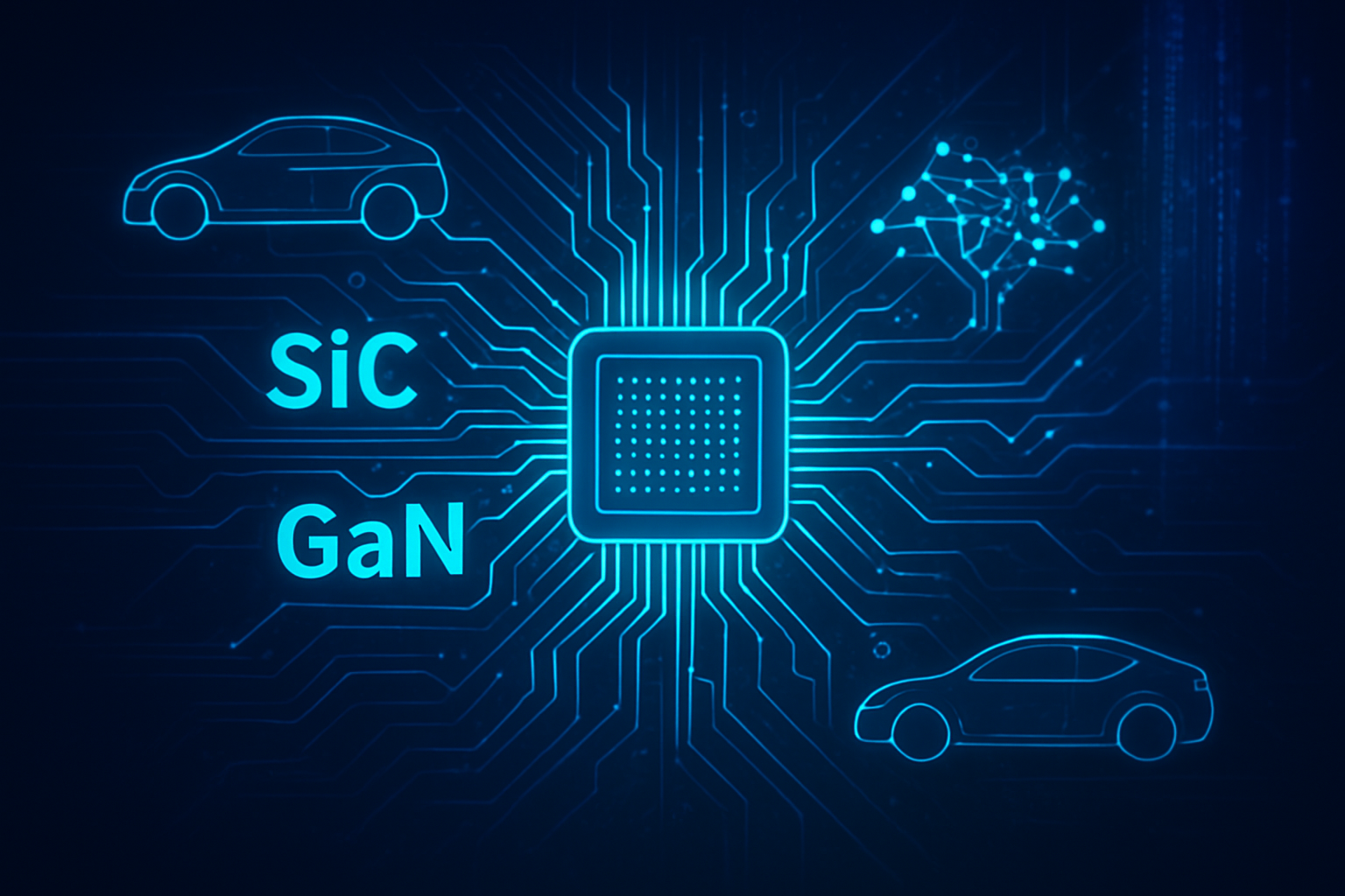
Technical Deep Dive: SiC, GaN, and the Rise of Analog Intelligence
The core of the current revolution in analog and industrial semiconductors lies in the strategic shift towards wide-bandgap (WBG) materials, primarily Silicon Carbide (SiC) and Gallium Nitride (GaN). These materials possess superior electrical properties compared to traditional silicon, allowing for operation at higher temperatures, voltages, and frequencies with significantly reduced energy losses and heat generation. This inherent advantage translates directly into more efficient power conversion, faster charging capabilities for EVs, and smaller, lighter power systems across industrial applications.
Specific details of these advancements are impressive. ON Semiconductor (NASDAQ: ON), for instance, has introduced its M3e EliteSiC MOSFETs, 1200V SiC devices that leverage planar technology to achieve industry-leading specific on-resistance while maintaining robust short-circuit capability. This pushes the boundaries of power density and efficiency, crucial for high-power applications. Similarly, their new Field Stop 7 (FS7) IGBT technology, integrated into 1200V half-bridge QDual3 IGBT modules, boasts a 33% increase in current density. This allows for the design of smaller, lighter, and more cost-effective power systems for demanding applications such as central solar inverters, energy storage, and heavy-duty commercial vehicles. Beyond power, ON Semiconductor's Hyperlux SG image sensors and Hyperlux ID family are revolutionizing indirect Time-of-Flight (iToF) depth sensing, extending accurate distance measurements and providing precise depth data on moving objects, vital for advanced robotics and autonomous systems.
A groundbreaking development from ON Semiconductor is their vertical GaN (vGaN) power semiconductors, built on novel GaN-on-GaN technology. Unlike traditional lateral GaN devices, vGaN conducts current vertically, setting new benchmarks for power density, efficiency, and ruggedness. This innovation can reduce energy loss by almost 50% and is particularly crucial for the demanding power requirements of AI data centers, EVs, renewable energy infrastructure, and industrial automation. This vertical architecture fundamentally differs from previous lateral approaches by enabling higher operating voltages and faster switching frequencies, overcoming some of the limitations of earlier GaN implementations and offering a direct path to higher performance and greater energy savings. The initial reactions from the industry and research community highlight the transformative potential of these WBG materials and vertical architectures, recognizing them as critical enablers for the next generation of high-power and high-frequency electronics.
The emergence of novel analog computing architectures, such as Analog Machine Learning (AnalogML), further distinguishes this wave of innovation. Companies like Aspinity are pioneering AnalogML platforms for ultra-low-power edge devices, enabling real-time data processing directly at the sensor level. This drastically reduces the need for extensive digital computation and data transfer, extending battery life and reducing latency in wearables, smart home devices, and industrial sensors. Furthermore, research into new analog processors that perform calculations directly within physical circuits, bypassing energy-intensive data transfers, is showing promise. A notable development from Peking University claims an analog AI chip capable of outperforming high-end GPUs by up to 1,000 times for certain AI tasks, while consuming significantly less energy. This "software programmable analog processor" addresses previous challenges of precision and programmability in analog systems, offering a potentially revolutionary approach to AI model training and future communication networks like 6G. These analog approaches represent a significant departure from purely digital processing, offering inherent advantages in power efficiency and speed for specific computational tasks, particularly at the edge.
Competitive Landscape and Market Dynamics
The ongoing advancements in analog and industrial semiconductors are reshaping the competitive landscape, creating new opportunities and challenges for tech giants, specialized AI labs, and burgeoning startups. Companies that heavily invest in and successfully deploy wide-bandgap (WBG) materials, advanced packaging, and novel analog computing solutions stand to gain significant strategic advantages.
Major players like ON Semiconductor (NASDAQ: ON), Infineon Technologies (ETR: IFX), STMicroelectronics (NYSE: STM), Texas Instruments (NASDAQ: TXN), and Analog Devices (NASDAQ: ADI) are poised to benefit immensely. ON Semiconductor, with its strong portfolio in SiC, vGaN, and sensing solutions, is particularly well-positioned to capitalize on the booming markets for EVs, AI data centers, and industrial automation. Their focus on high-efficiency power management and advanced sensing directly addresses critical needs in these high-growth sectors. Similarly, Infineon's investments in SiC and their collaboration with NVIDIA (NASDAQ: NVDA) on 800V DC power delivery for AI data centers highlight the strategic importance of these foundational technologies. Texas Instruments, a long-standing leader in analog, continues to expand its manufacturing capacity, particularly with new 300mm fabs, to meet the surging demand across industrial and automotive applications.
This development also has significant competitive implications. Companies that lag in adopting WBG materials or fail to innovate in power management and sensor integration may find their products less competitive in terms of efficiency, size, and cost. The superior performance of SiC and GaN, for instance, can render older silicon-based power solutions less attractive for new designs, potentially disrupting established product lines. For AI labs and tech companies, access to highly efficient power management solutions and innovative analog computing architectures is crucial. The ability to power AI data centers with reduced energy consumption directly impacts operational costs and sustainability goals. Furthermore, the rise of AnalogML and edge AI, enabled by these semiconductors, could shift some processing away from centralized cloud infrastructure, potentially disrupting traditional cloud-centric AI models and empowering a new generation of intelligent edge devices.
Market positioning is increasingly defined by a company's ability to offer integrated, high-performance, and energy-efficient solutions. Strategic partnerships, like Analog Devices' expanded collaboration with General Motors (NYSE: GM) for EV battery management systems, underscore the importance of deep industry integration. Companies that can provide comprehensive solutions, from power conversion to sensing and processing, will command a stronger position. The increasing complexity and specialization within the semiconductor industry also mean that startups focusing on niche areas, such as advanced analog computing for specific AI tasks or ultra-low-power edge processing, can carve out significant market shares by offering highly specialized and optimized solutions that complement the broader offerings of larger players.
Wider Significance: Fueling the Intelligent and Electric Future
The advancements in analog and industrial semiconductors represent more than just incremental improvements; they are foundational to the broader technological landscape and critical enablers for the most significant trends shaping our future. This wave of innovation fits perfectly into the overarching drive towards greater energy efficiency, pervasive intelligence, and sustainable electrification.
The impact is far-reaching. In the context of the global energy transition, these semiconductors are indispensable. Wide-bandgap materials like SiC and GaN are directly contributing to the efficiency of electric vehicles, making them more practical and accessible by extending range and accelerating charging times. In renewable energy, they optimize power conversion in solar inverters and wind turbines, maximizing energy capture and integration into smart grids. For AI, the ability to power data centers with significantly reduced energy consumption is paramount, addressing a major environmental concern associated with the exponential growth of AI processing. Furthermore, the development of AnalogML and novel analog computing architectures is pushing intelligence to the very edge of networks, enabling real-time decision-making in IIoT devices and autonomous systems without relying on constant cloud connectivity, thereby enhancing responsiveness and data privacy.
Potential concerns, however, include the complexity and cost associated with transitioning to new materials and manufacturing processes. The supply chain for SiC and GaN, while maturing, still faces challenges in scaling to meet exploding demand. Geopolitical tensions and the increasing strategic importance of semiconductor manufacturing also raise concerns about supply chain resilience and national security. Compared to previous AI milestones, where the focus was often on algorithmic breakthroughs or increases in computational power through traditional silicon, this current wave highlights the critical role of the underlying hardware infrastructure. It underscores that the future of AI is not solely about software; it is deeply intertwined with the physical limitations and capabilities of the chips that power it. These semiconductor innovations are as significant as past breakthroughs in processor architecture, as they unlock entirely new paradigms for power efficiency and localized intelligence, which are essential for the widespread deployment of AI in the real world.
The Road Ahead: Anticipating Future Developments
Looking ahead, the trajectory of analog and industrial semiconductors promises continued evolution and groundbreaking applications. Near-term developments are expected to focus on further refinements of wide-bandgap (WBG) materials, with ongoing research aimed at increasing voltage capabilities, reducing manufacturing costs, and improving the reliability and robustness of SiC and GaN devices. We can anticipate more integrated power modules that combine multiple WBG components into compact, highly efficient packages, simplifying design for engineers and accelerating adoption across industries.
In the long term, the field will likely see a deeper convergence of analog and digital processing, especially at the edge. The promise of fully programmable analog AI chips, moving beyond specialized functions to more general-purpose analog computation, could revolutionize how AI models are trained and deployed, offering unprecedented energy efficiency for inference and even training directly on edge devices. Research into new materials beyond SiC and GaN, and novel device architectures that push the boundaries of quantum effects, may also emerge, offering even greater performance and efficiency gains.
Potential applications and use cases on the horizon are vast. Beyond current applications, these advancements will enable truly autonomous systems that can operate for extended periods on minimal power, intelligent infrastructure that self-optimizes, and a new generation of medical devices that offer continuous, unobtrusive monitoring. The enhanced precision and reliability of industrial sensors, coupled with edge AI, will drive further automation and predictive maintenance in factories, smart cities, and critical infrastructure. Challenges that need to be addressed include the standardization of new manufacturing processes, the development of robust design tools for complex analog-digital hybrid systems, and the education of a workforce capable of designing and implementing these advanced technologies. Supply chain resilience will remain a critical focus, with continued investments in regional manufacturing capabilities.
Experts predict that the relentless pursuit of energy efficiency and distributed intelligence will continue to be the primary drivers. The move towards "more than Moore" – integrating diverse functionalities beyond just logic – will see analog, power, and sensing capabilities increasingly co-packaged or integrated onto single chips. What experts predict will happen next is a continued acceleration in the adoption of SiC and GaN across all power-hungry applications, coupled with significant breakthroughs in analog computing that allow AI to become even more pervasive, efficient, and embedded into the fabric of our physical world.
Comprehensive Wrap-Up: A Foundation for Future Innovation
The current wave of innovation in analog and industrial semiconductors represents a pivotal moment in technological advancement. Key takeaways include the transformative power of wide-bandgap materials like Silicon Carbide and Gallium Nitride in achieving unprecedented energy efficiency and power density, the critical role of advanced packaging and vertical architectures in miniaturization and performance, and the emerging potential of novel analog computing to bring ultra-low-power intelligence to the edge. Companies such as ON Semiconductor (NASDAQ: ON) are not just participating in this shift; they are actively shaping it with their breakthrough technologies in power management, sensing, and material science.
This development's significance in AI history, and indeed in the broader history of technology, cannot be overstated. It underscores that the advancements in AI are inextricably linked to the underlying hardware that powers them. Without these efficient and intelligent semiconductor foundations, the ambitious goals of widespread AI deployment, sustainable electrification, and pervasive connectivity would remain largely out of reach. These innovations are not merely supporting existing technologies; they are enabling entirely new paradigms of operation, making previously impossible applications feasible.
Final thoughts on the long-term impact point to a future where technology is not only more powerful but also significantly more sustainable and integrated into our daily lives. Reduced energy consumption in data centers and EVs will have a tangible positive impact on climate change efforts, while distributed intelligence will lead to safer, more efficient, and more responsive autonomous systems and industrial operations. The continuous push for miniaturization and efficiency will also drive innovation in personal electronics, medical devices, and smart infrastructure, making technology more accessible and less intrusive.
In the coming weeks and months, we should watch for continued announcements regarding new product launches utilizing SiC and GaN in automotive and industrial sectors, further investments in manufacturing capacity by key players, and the emergence of more concrete applications leveraging analog AI at the edge. The synergy between these semiconductor advancements and the rapidly evolving fields of AI, IoT, and electrification will undoubtedly continue to generate exciting and impactful developments that reshape our technological landscape.
This content is intended for informational purposes only and represents analysis of current AI developments.
TokenRing AI delivers enterprise-grade solutions for multi-agent AI workflow orchestration, AI-powered development tools, and seamless remote collaboration platforms.
For more information, visit https://www.tokenring.ai/.