Tag: Silicon

  • The Silicon Sovereignty: How 2026’s Edge AI Chips are Liberating LLMs from the Cloud

    The Silicon Sovereignty: How 2026’s Edge AI Chips are Liberating LLMs from the Cloud

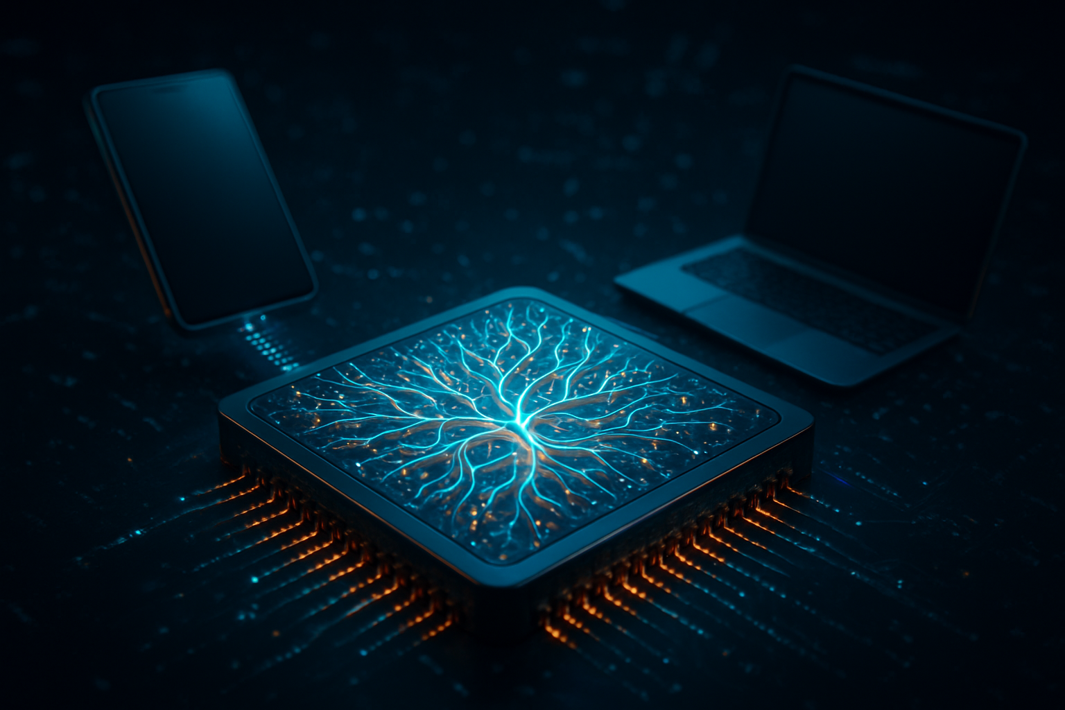
    The era of "Cloud-First" artificial intelligence is officially coming to a close. As of early 2026, the tech industry has reached a pivotal inflection point where the intelligence once reserved for massive server farms now resides comfortably within the silicon of our smartphones and laptops. This shift, driven by a fierce arms race between Apple (NASDAQ:AAPL), Qualcomm (NASDAQ:QCOM), and MediaTek (TWSE:2454), has transformed the Neural Processing Unit (NPU) from a niche marketing term into the most critical component of modern computing.

    The immediate significance of this transition cannot be overstated. By running Large Language Models (LLMs) locally, devices are no longer mere windows into a remote brain; they are the brain. This movement toward "Edge AI" has effectively solved the "latency-privacy-cost" trilemma that plagued early generative AI applications. Users are now interacting with autonomous AI agents that can draft emails, analyze complex spreadsheets, and generate high-fidelity media in real-time—all without an internet connection and without ever sending a single byte of private data to a third-party server.

    The Architecture of Autonomy: NPU Breakthroughs in 2026

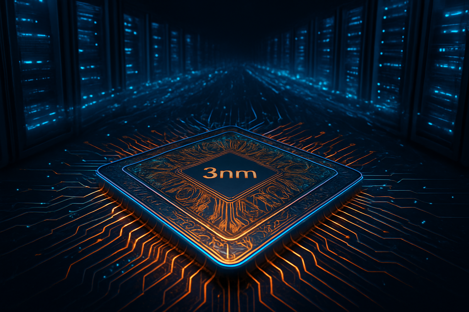
    The technical landscape of 2026 is dominated by three flagship silicon architectures that have redefined on-device performance. Apple has moved beyond the traditional standalone Neural Engine with its A19 Pro chip. Built on TSMC’s (NYSE:TSM) refined N3P 3nm process, the A19 Pro introduces "Neural Accelerators" integrated directly into the GPU cores. This hybrid approach provides a combined AI throughput of approximately 75 TOPS (Trillions of Operations Per Second), allowing the iPhone 17 Pro to run 8-billion parameter models at over 20 tokens per second. By fusing matrix multiplication units into the graphics pipeline, Apple has achieved a 4x increase in AI compute power over the previous generation, making local LLM execution feel as instantaneous as a local search.

    Qualcomm has countered with the Snapdragon 8 Elite Gen 5, a chip designed specifically for what the industry now calls "Agentic AI." The new Hexagon NPU delivers 80 TOPS of dedicated AI performance, but the real innovation lies in the Oryon CPU cores, which now feature hardware-level matrix acceleration to assist in the "pre-fill" stage of LLM processing. This allows the device to handle complex "Personal Knowledge Graphs," enabling the AI to learn user habits locally and securely. Meanwhile, MediaTek has claimed the raw performance crown with the Dimensity 9500. Its NPU 990 is the first mobile processor to reach 100 TOPS, utilizing "Compute-in-Memory" (CIM) technology. By embedding AI compute units directly within the memory cache, MediaTek has slashed the power consumption of always-on AI models by over 50%, a critical feat for battery-conscious mobile users.

    These advancements represent a radical departure from the "NPU-as-an-afterthought" era of 2023 and 2024. Previous approaches relied on the cloud for any task involving more than basic image recognition or voice-to-text. Today’s silicon is optimized for 4-bit and even 1.58-bit (binary) quantization, allowing massive models to be compressed into a fraction of their original size without losing significant intelligence. Industry experts have noted that the arrival of LPDDR6 memory in early 2026—offering speeds up to 14.4 Gbps—has finally broken the "memory wall," allowing mobile devices to handle the high-bandwidth requirements of 30B+ parameter models that were once the exclusive domain of desktop workstations.

    Strategic Realignment: The Hardware Supercycle and the Cloud Threat

    This silicon revolution has sparked a massive hardware supercycle, with "AI PCs" now projected to account for 55% of all personal computer sales by the end of 2026. For hardware giants like Apple and Qualcomm, the strategy is clear: commoditize the AI model to sell more expensive, high-margin silicon. As local models become "good enough" for 90% of consumer tasks, the strategic advantage shifts from the companies training the models to the companies controlling the local execution environment. This has led to a surge in demand for devices with 16GB or even 24GB of RAM as the baseline, driving up average selling prices and revitalizing a smartphone market that had previously reached a plateau.

    For cloud-based AI titans like Microsoft (NASDAQ:MSFT) and Google (NASDAQ:GOOGL), the rise of Edge AI is a double-edged sword. While it reduces the immense inference costs associated with running billions of free AI queries on their servers, it also threatens their subscription-based revenue models. If a user can run a highly capable version of Llama-3 or Gemini Nano locally on their Snapdragon-powered laptop, the incentive to pay for a monthly "Pro" AI subscription diminishes. In response, these companies are pivoting toward "Hybrid AI" architectures, where the local NPU handles immediate, privacy-sensitive tasks, while the cloud is reserved for "Heavy Reasoning" tasks that require trillion-parameter models.

    The competitive implications are particularly stark for startups and smaller AI labs. The shift to local silicon favors open-source models that can be easily optimized for specific NPUs. This has inadvertently turned the hardware manufacturers into the new gatekeepers of the AI ecosystem. Apple’s "walled garden" approach, for instance, now extends to the "Neural Engine" layer, where developers must use Apple’s proprietary CoreML tools to access the full speed of the A19 Pro. This creates a powerful lock-in effect, as the best AI experiences become inextricably tied to the specific capabilities of the underlying silicon.

    Sovereignty and Sustainability: The Wider Significance of the Edge

    Beyond the balance sheets, the move to Edge AI marks a significant milestone in the history of data privacy. We are entering an era of "Sovereign AI," where sensitive personal, medical, and financial data never leaves the user's pocket. In a world increasingly concerned with data breaches and corporate surveillance, the ability to run a sophisticated AI assistant entirely offline is a powerful selling point. This has significant implications for enterprise security, allowing employees to use generative AI tools on proprietary codebases or confidential legal documents without the risk of data leakage to a cloud provider.

    The environmental impact of this shift is equally profound. Data centers are notorious energy hogs, requiring vast amounts of electricity for both compute and cooling. By shifting the inference workload to highly efficient mobile NPUs, the tech industry is significantly reducing its carbon footprint. Research indicates that running a generative AI task on a local NPU can be up to 30 times more energy-efficient than routing that same request through a global network to a centralized server. As global energy prices remain volatile in 2026, the efficiency of the "Edge" has become a matter of both environmental and economic necessity.

    However, this transition is not without its concerns. The "Memory Wall" and the rising cost of advanced semiconductors have created a new digital divide. As TSMC’s 2nm wafers reportedly cost 50% more than their 3nm predecessors, the most advanced AI features are being locked behind a "premium paywall." There is a growing risk that the benefits of local, private AI will be reserved for those who can afford $1,200 smartphones and $2,000 laptops, while users on budget hardware remain reliant on cloud-based systems that may monetize their data in exchange for access.

    The Road to 2nm: What Lies Ahead for Edge Silicon

    Looking forward, the industry is already bracing for the transition to 2nm process technology. TSMC and Intel (NASDAQ:INTC) are expected to lead this charge using Gate-All-Around (GAA) nanosheet transistors, which promise another 25-30% reduction in power consumption. This will be critical as the next generation of Edge AI moves toward "Multimodal-Always-On" capabilities—where the device’s NPU is constantly processing live video and audio feeds to provide proactive, context-aware assistance.

    The next major hurdle is the "Thermal Ceiling." As NPUs become more powerful, managing the heat generated by sustained AI workloads in a thin smartphone chassis is becoming a primary engineering challenge. We are likely to see a new wave of innovative cooling solutions, from active vapor chambers to specialized thermal interface materials, becoming standard in consumer electronics. Furthermore, the arrival of LPDDR6 memory in late 2026 is expected to double the available bandwidth, potentially making 70B-parameter models—currently the gold standard for high-level reasoning—usable on high-end laptops and tablets.

    Experts predict that by 2027, the distinction between "AI" and "non-AI" software will have entirely vanished. Every application will be an AI application, and the NPU will be as fundamental to the computing experience as the CPU was in the 1990s. The focus will shift from "can it run an LLM?" to "how many autonomous agents can it run simultaneously?" This will require even more sophisticated task-scheduling silicon that can balance the needs of multiple competing AI models without draining the battery in a matter of hours.

    Conclusion: A New Chapter in the History of Computing

    The developments of early 2026 represent a definitive victory for the decentralized model of artificial intelligence. By successfully shrinking the power of an LLM to fit onto a piece of silicon the size of a fingernail, Apple, Qualcomm, and MediaTek have fundamentally changed our relationship with technology. The NPU has liberated AI from the constraints of the cloud, bringing with it unprecedented gains in privacy, latency, and energy efficiency.

    As we look back at the history of AI, the year 2026 will likely be remembered as the year the "Ghost in the Machine" finally moved into the machine itself. The strategic shift toward Edge AI has not only triggered a massive hardware replacement cycle but has also forced the world’s most powerful software companies to rethink their business models. In the coming months, watch for the first wave of "LPDDR6-ready" devices and the initial benchmarks of the 2nm "GAA" prototypes, which will signal the next leap in this ongoing silicon revolution.


    This content is intended for informational purposes only and represents analysis of current AI developments.

    TokenRing AI delivers enterprise-grade solutions for multi-agent AI workflow orchestration, AI-powered development tools, and seamless remote collaboration platforms.
    For more information, visit https://www.tokenring.ai/.

  • The Silicon Sovereignty Era: Hyperscalers Break NVIDIA’s Grip with 3nm Custom AI Chips

    The Silicon Sovereignty Era: Hyperscalers Break NVIDIA’s Grip with 3nm Custom AI Chips

    The dawn of 2026 has brought a seismic shift to the artificial intelligence landscape, as the world’s largest cloud providers—the hyperscalers—have officially transitioned from being NVIDIA’s (NASDAQ: NVDA) biggest customers to its most formidable architectural rivals. For years, the industry operated under a "one-size-fits-all" GPU paradigm, but a new surge in custom Application-Specific Integrated Circuits (ASICs) has shattered that consensus. Driven by the relentless demand for more efficient inference and the staggering costs of frontier model training, Google, Amazon, and Meta have unleashed a new generation of 3nm silicon that is fundamentally rewriting the economics of AI.

    At the heart of this revolution is a move toward vertical integration that rivals the early days of the mainframe. By designing their own chips, these tech giants are no longer just buying compute; they are engineering it to fit the specific contours of their proprietary models. This strategic pivot is delivering 30% to 40% better price-performance for internal workloads, effectively commoditizing high-end AI compute and providing a critical buffer against the supply chain bottlenecks and premium margins that have defined the NVIDIA era.

    The 3nm Power Play: Ironwood, Trainium3, and the Scaling of MTIA

    The technical specifications of this new silicon class are nothing short of breathtaking. Leading the charge is Google, a subsidiary of Alphabet Inc. (NASDAQ: GOOGL), with its TPU v7p (Ironwood). Built on Taiwan Semiconductor Manufacturing Company’s (NYSE: TSM) cutting-edge 3nm (N3P) process, Ironwood is a dual-chiplet powerhouse featuring a massive 192GB of HBM3E memory. With a memory bandwidth of 7.4 TB/s and a peak performance of 4.6 PFLOPS of dense FP8 compute, the TPU v7p is designed specifically for the "age of inference," where massive context windows and complex reasoning are the new standard. Google has already moved into mass deployment, reporting that over 75% of its Gemini model computations are now handled by its internal TPU fleet.

    Not to be outdone, Amazon.com, Inc. (NASDAQ: AMZN) has officially ramped up production of AWS Trainium3. Also utilizing the 3nm process, Trainium3 packs 144GB of HBM3E and delivers 2.52 PFLOPS of FP8 performance per chip. What sets the AWS offering apart is its "UltraServer" configuration, which interconnects 144 chips into a single, liquid-cooled rack capable of matching NVIDIA’s Blackwell architecture in rack-level performance while offering a significantly more efficient power profile. Meanwhile, Meta Platforms, Inc. (NASDAQ: META) is scaling its Meta Training and Inference Accelerator (MTIA). While its current v2 "Artemis" chips focus on offloading recommendation engines from GPUs, Meta’s 2026 roadmap includes its first dedicated in-house training chip, designed to support the development of Llama 4 and beyond within its massive "Titan" data center clusters.

    These advancements represent a departure from the general-purpose nature of the GPU. While an NVIDIA H100 or B200 is designed to be excellent at almost any parallel task, these custom ASICs are "leaner." By stripping away legacy components and focusing on specific data formats like MXFP8 and MXFP4, and optimizing for specific software frameworks like PyTorch (for Meta) or JAX (for Google), these chips achieve higher throughput per watt. The integration of advanced liquid cooling and proprietary interconnects like Google’s Optical Circuit Switching (OCS) allows these chips to operate in unified domains of nearly 10,000 units, creating a level of "cluster-scale" efficiency that was previously unattainable.

    Disrupting the Monopoly: Market Implications for the GPU Giants

    The immediate beneficiaries of this silicon surge are the hyperscalers themselves, who can now offer AI services at a fraction of the cost of their competitors. AWS has already begun using Trainium3 as a "bargaining chip," implementing price cuts of up to 45% on its NVIDIA-based instances to remain competitive with its own internal hardware. This internal competition is a nightmare scenario for NVIDIA’s margins. While the AI pioneer still dominates the high-end training market, the shift toward inference—projected to account for 70% of all AI workloads in 2026—plays directly into the hands of custom ASIC designers who can optimize for the specific latency and throughput requirements of a deployed model.

    The ripple effects extend to the "enablers" of this custom silicon wave: Broadcom Inc. (NASDAQ: AVGO) and Marvell Technology, Inc. (NASDAQ: MRVL). Broadcom has emerged as the undisputed leader in the custom ASIC space, acting as the primary design partner for Google’s TPUs and Meta’s MTIA. Analysts project Broadcom’s AI semiconductor revenue will hit a staggering $46 billion in 2026, driven by a $73 billion backlog of orders from hyperscalers and firms like Anthropic. Marvell, meanwhile, has secured its place by partnering with AWS on Trainium and Microsoft Corporation (NASDAQ: MSFT) on its Maia accelerators. These design firms provide the critical IP blocks—such as high-speed SerDes and memory controllers—that allow cloud giants to bring chips to market in record time.

    For the broader tech industry, this development signals a fracturing of the AI hardware market. Startups and mid-sized enterprises that were once priced out of the NVIDIA ecosystem are finding a new home in "capacity blocks" of custom silicon. By commoditizing the underlying compute, the hyperscalers are shifting the competitive focus away from who has the most GPUs and toward who has the best data and the most efficient model architectures. This "Silicon Sovereignty" allows the likes of Google and Meta to insulate themselves from the "NVIDIA Tax," ensuring that their massive capital expenditures translate more directly into shareholder value rather than flowing into the coffers of a single hardware vendor.

    A New Architectural Paradigm: Beyond the GPU

    The surge of custom silicon is more than just a cost-saving measure; it is a fundamental shift in the AI landscape. We are moving away from a world where software was written to fit the hardware, and into an era of "hardware-software co-design." When Meta develops a chip in tandem with the PyTorch framework, or Google optimizes its TPU for the Gemini architecture, they achieve a level of vertical integration that mirrors Apple’s success with its M-series silicon. This trend suggests that the "one-size-fits-all" approach of the general-purpose GPU may eventually be relegated to the research lab, while production-scale AI is handled by highly specialized, purpose-built machines.

    However, this transition is not without its concerns. The rise of proprietary silicon could lead to a "walled garden" effect in AI development. If a model is trained and optimized specifically for Google’s TPU v7p, moving that workload to AWS or an on-premise NVIDIA cluster becomes a non-trivial engineering challenge. There are also environmental implications; while these chips are more efficient per token, the sheer scale of deployment is driving unprecedented energy demands. The "Titan" clusters Meta is building in 2026 are gigawatt-scale projects, raising questions about the long-term sustainability of the AI arms race and the strain it puts on national power grids.

    Comparing this to previous milestones, the 2026 silicon surge feels like the transition from CPU-based mining to ASICs in the early days of Bitcoin—but on a global, industrial scale. The era of experimentation is over, and the era of industrial-strength, optimized production has begun. The breakthroughs of 2023 and 2024 were about what AI could do; the breakthroughs of 2026 are about how AI can be delivered to billions of people at a sustainable cost.

    The Horizon: What Comes After 3nm?

    Looking ahead, the roadmap for custom silicon shows no signs of slowing down. As we move toward 2nm and beyond, the focus is expected to shift from raw compute power to "advanced packaging" and "photonic interconnects." Marvell and Broadcom are already experimenting with 3.5D packaging and optical I/O, which would allow chips to communicate at the speed of light, effectively turning an entire data center into a single, giant processor. This would solve the "memory wall" that currently limits the size of the models we can train.

    In the near term, expect to see these custom chips move deeper into the "edge." While 2026 is the year of the data center ASIC, 2027 and 2028 will likely see these same architectures scaled down for use in "AI PCs" and autonomous vehicles. The challenges remain significant—particularly in the realm of software compilers that can automatically optimize code for diverse hardware targets—but the momentum is undeniable. Experts predict that by the end of the decade, over 60% of all AI compute will run on non-NVIDIA hardware, a total reversal of the market dynamics we saw just three years ago.

    Closing the Loop on Custom Silicon

    The mass deployment of Google’s TPU v7p, AWS’s Trainium3, and Meta’s MTIA marks the definitive end of the GPU’s undisputed reign. By taking control of their silicon destiny, the hyperscalers have not only reduced their reliance on a single vendor but have also unlocked a new level of performance that will enable the next generation of "Agentic AI" and trillion-parameter reasoning models. The 30-40% price-performance advantage of these ASICs is the new baseline for the industry, forcing every player in the ecosystem to innovate or be left behind.

    As we move through 2026, the key metrics to watch will be the "utilization rates" of these custom clusters and the speed at which third-party developers adopt the proprietary software stacks required to run on them. The "Silicon Sovereignty" era is here, and it is defined by a simple truth: in the age of AI, the most powerful software is only as good as the silicon it was born to run on. The battle for the future of intelligence is no longer just being fought in the cloud—it’s being fought in the transistor.


    This content is intended for informational purposes only and represents analysis of current AI developments.

    TokenRing AI delivers enterprise-grade solutions for multi-agent AI workflow orchestration, AI-powered development tools, and seamless remote collaboration platforms.
    For more information, visit https://www.tokenring.ai/.