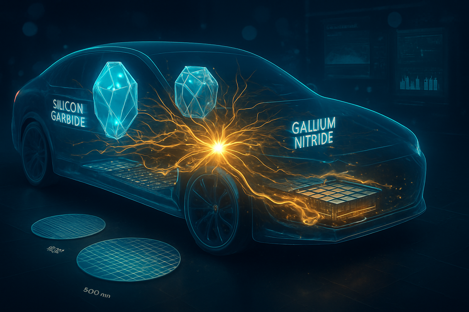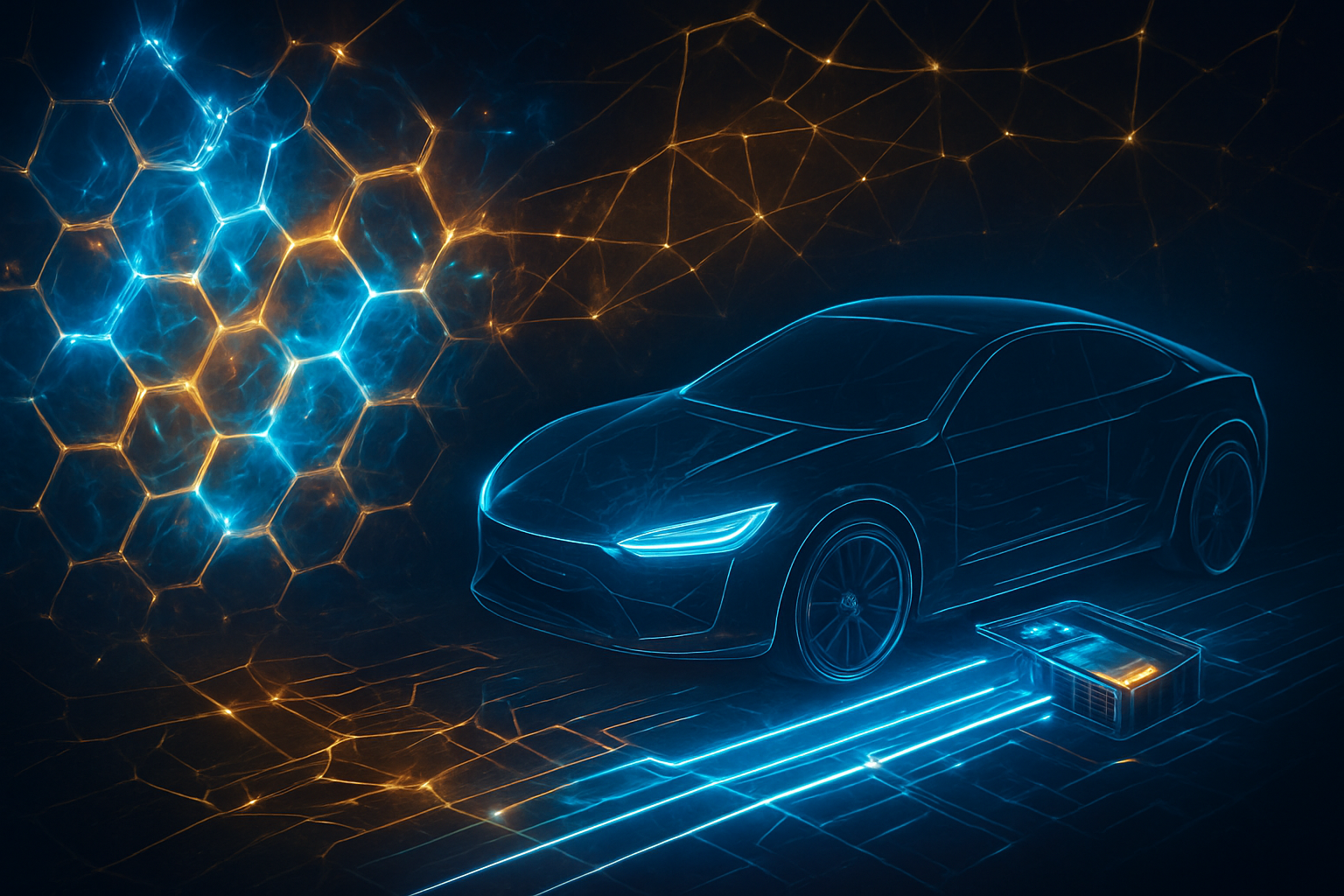
As of February 2, 2026, the global transition to sustainable transport has reached a critical hardware bottleneck: the limits of traditional silicon. While passenger electric vehicles (EVs) have spent the last decade proving the viability of lithium-ion batteries, the heavy-duty sector—comprising Class 8 trucks, buses, and mining equipment—is undergoing a deeper architectural shift. At the heart of this transformation is Silicon Carbide (SiC), a wide-bandgap semiconductor that has officially transitioned from a luxury component to the industrial backbone of heavy-duty electrification. Recent market data now projects that the market for SiC inverters specifically for heavy vehicles will swell to $5.8 billion by 2033, a nearly five-fold increase from 2024 levels.
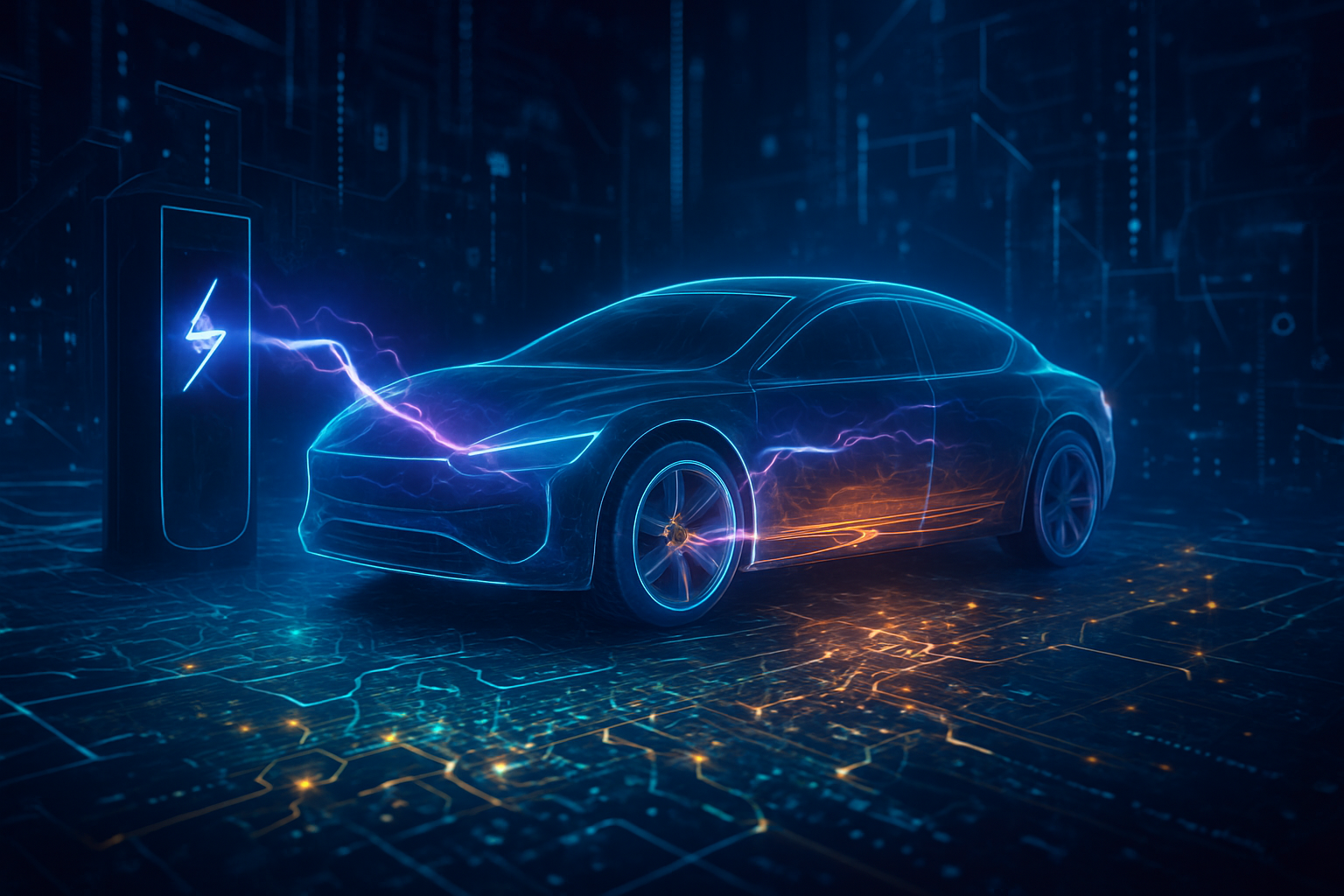
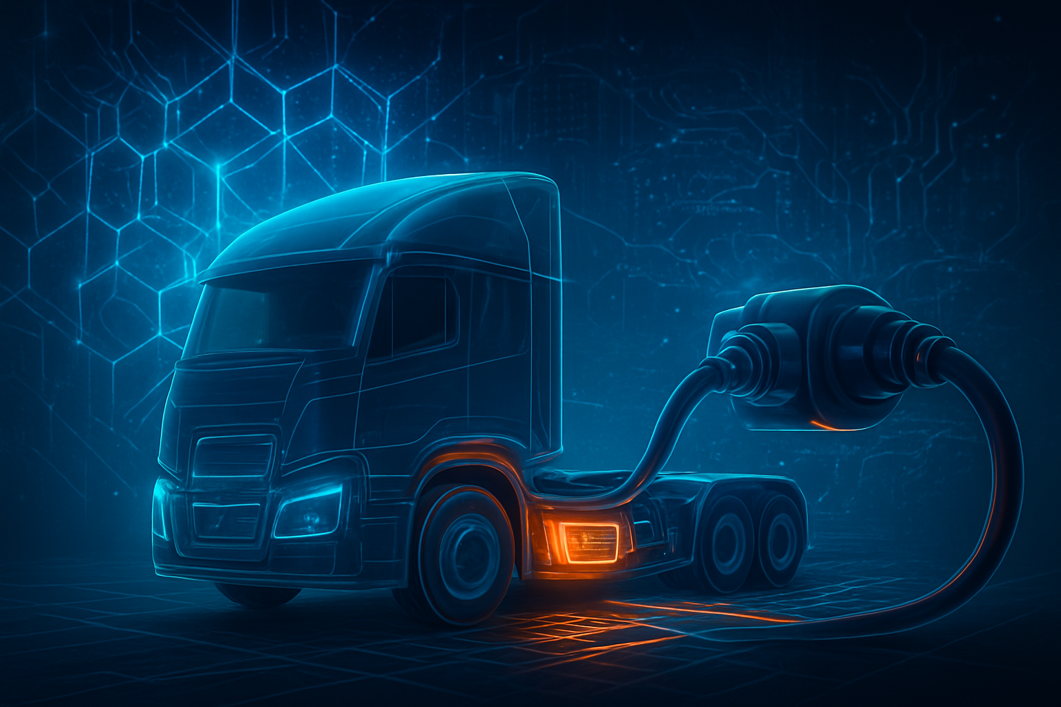
This development is more than just a material swap; it represents the enabling technology for Megawatt Charging Systems (MCS) and ultra-high-voltage architectures. For fleet operators, the shift to SiC is the difference between an electric truck that is a logistical liability and one that rivals the range and uptime of diesel. As the industry moves toward 800V and even 1200V systems to facilitate faster charging, traditional Silicon Insulated-Gate Bipolar Transistors (IGBTs) are hitting a physical ceiling. SiC's ability to operate at higher temperatures and frequencies is not just an incremental improvement—it is the catalyst for the next generation of autonomous, AI-managed logistical networks.
Technical Superiority: Breaking the 800V Barrier
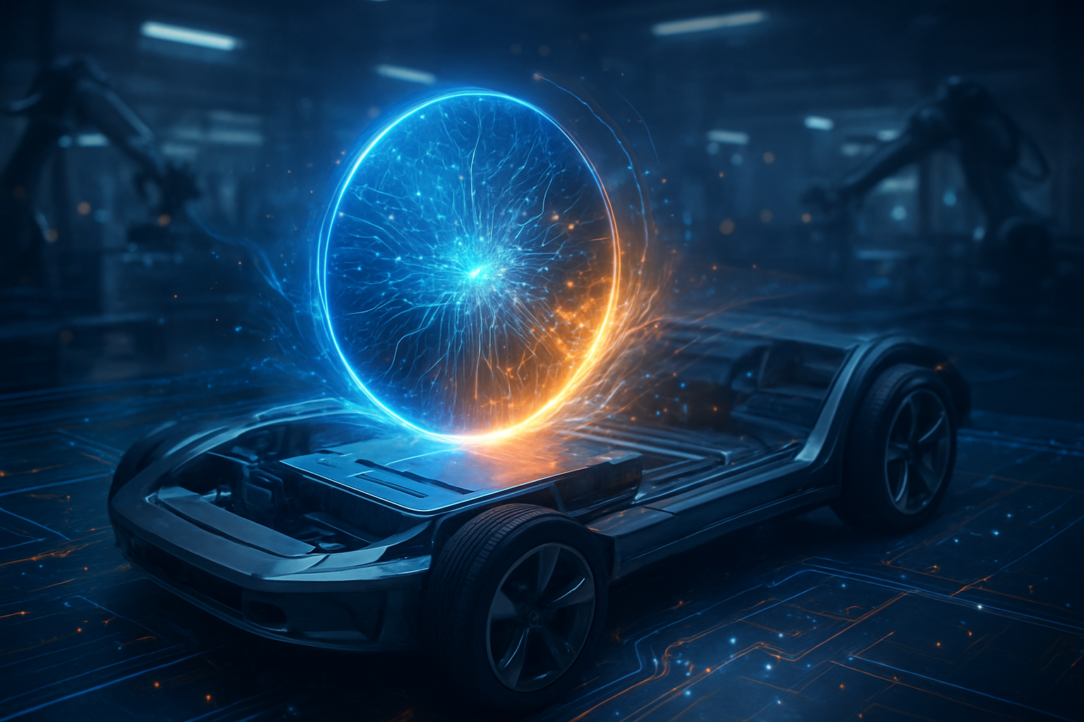
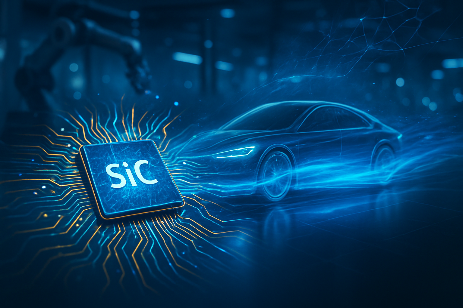
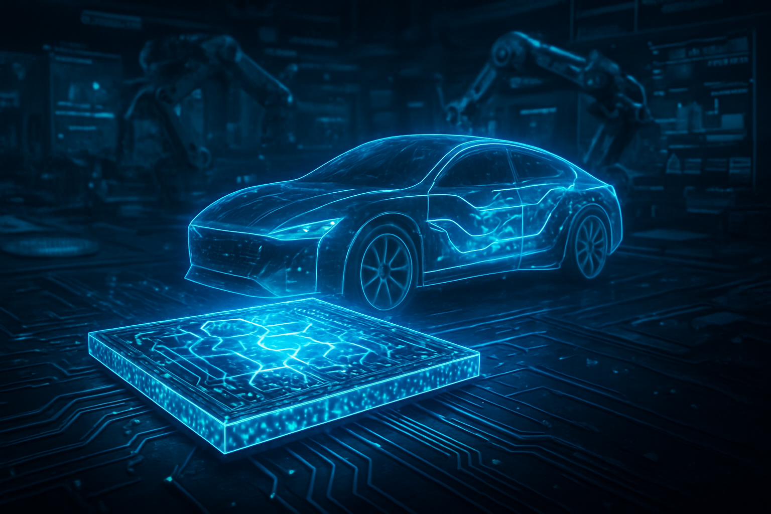
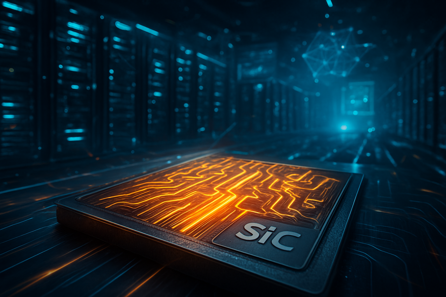
The technical shift toward Silicon Carbide is driven by its "wide bandgap" properties, which allow electrons to jump from the valence band to the conduction band with significantly more energy than in standard silicon. This translates to a breakdown field ten times higher than that of traditional silicon, allowing SiC dies to be much thinner and more efficient at handling the high voltages required by heavy-duty EVs. In early 2026, we are seeing the mainstream adoption of 1200V SiC modules, which are essential for the Megawatt Charging Systems currently being rolled out by industry leaders. These systems can deliver between 750 kW and 3.75 MW of power, charging a 500kWh battery in under 20 minutes—a feat that would cause standard silicon inverters to suffer catastrophic thermal failure.
Beyond voltage handling, SiC’s primary advantage lies in its drastically reduced switching losses. Technical specifications from leading manufacturers show that SiC can reduce power dissipation by as much as 70% compared to IGBTs. For a heavy-duty truck like those produced by Volvo Group (OTCMKTS: VLVLY) or Daimler Truck (OTCMKTS: DTRUY), this efficiency gain directly translates to a 5% to 10% increase in total vehicle range. Furthermore, because SiC operates efficiently at higher switching frequencies, engineers can utilize smaller passive components, such as inductors and capacitors. This leads to a 40% reduction in the cooling system's volume and weight, allowing for higher payloads and more streamlined vehicle designs.
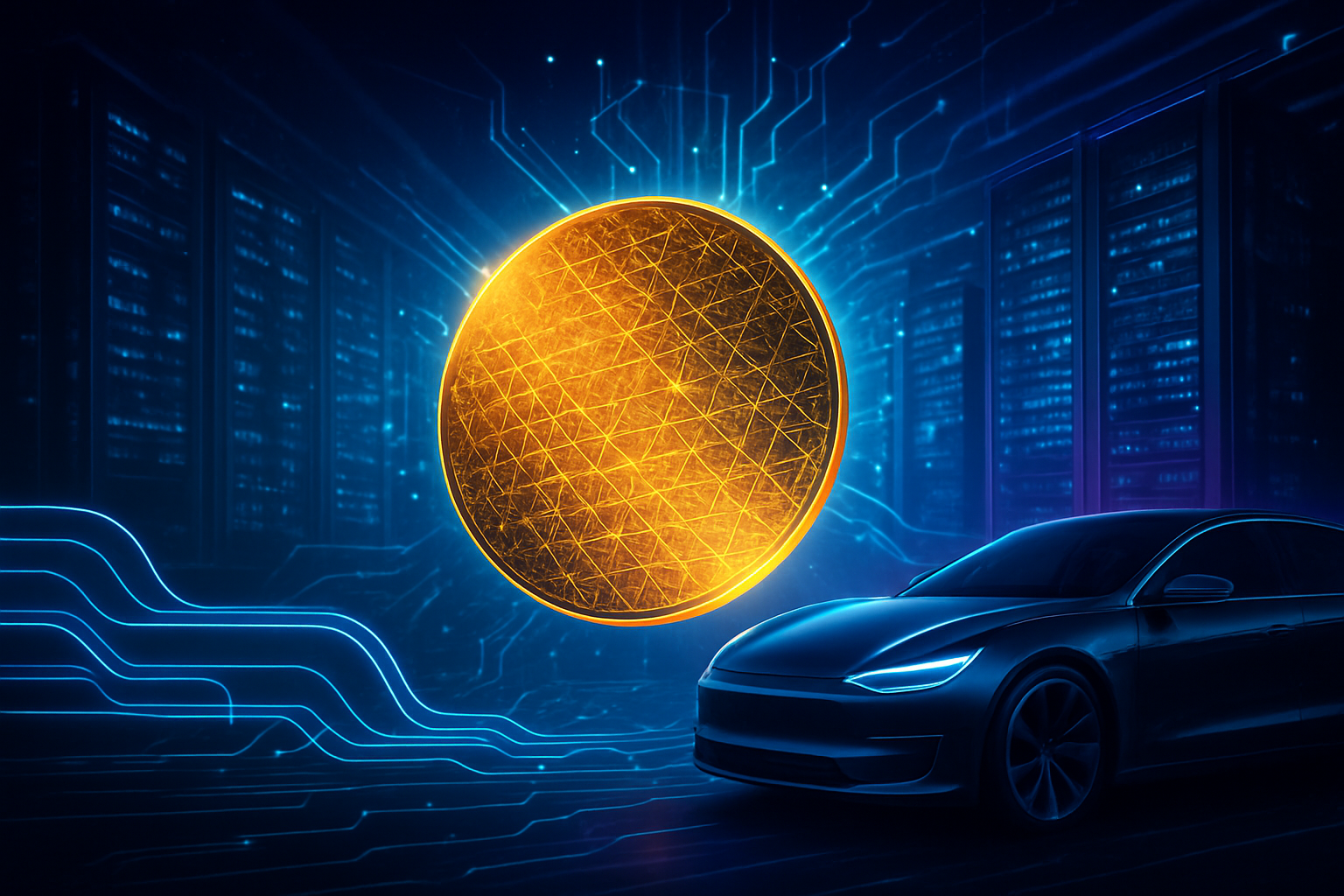
The initial reactions from the power electronics community have been overwhelmingly positive, though not without caution regarding supply chain resilience. Experts at the 2025 Power Electronics Conference noted that while the "physics of SiC is undeniable," the manufacturing process remains complex. Unlike silicon ingots, which can be grown in days, SiC crystals take weeks to mature and are prone to defects. However, the introduction of 200mm (8-inch) and the first experimental 300mm (12-inch) wafers in early 2026 is beginning to address these yield issues, promising a future of lower costs and higher availability for the mass market.
The Competitive Landscape: Giants and Challengers
The surge in SiC demand has reshaped the semiconductor landscape. STMicroelectronics (NYSE: STM) remains the dominant force in the automotive SiC market, holding a 32.6% market share as of early 2026. Their strategic vertical integration, bolstered by their new high-volume facility in Catania, Italy, has allowed them to maintain a firm grip on high-volume contracts with major EV makers like Tesla (NASDAQ: TSLA). Meanwhile, onsemi (NASDAQ: ON) has solidified its position as the number two player. Following its 2024-2025 expansion of the EliteSiC line, onsemi has achieved over 50% self-sufficiency in substrate materials, a move that provides them a significant buffer against the supply shocks that plagued the industry earlier this decade.
Infineon Technologies (OTCMKTS: IFNNY) has taken a slightly different strategic path, focusing on a "diversified supplier" model. While they successfully transitioned to 200mm wafers in 2025, they continue to source substrates from multiple partners to mitigate risk. This approach has won them significant design wins among European heavy-duty OEMs. Perhaps the most dramatic story of the year is the resurgence of Wolfspeed (NYSE: WOLF). After undergoing a strategic Chapter 11 restructuring in late 2025 to clear debt and refocus on its core strengths, Wolfspeed has entered 2026 with a massive equity partnership with Renesas (OTCMKTS: RNECY). They remain the world’s largest producer of SiC substrates, and their pivot toward becoming a pure-play SiC materials and device giant is seen as a high-stakes bet on the $5.8 billion heavy-vehicle milestone.
The competition is no longer just about who can make the most chips, but who can integrate them into the most efficient power modules. This has led to a wave of vertical partnerships. Trucking giants like Scania, a subsidiary of the Traton Group (OTCMKTS: TRATF), are now co-developing SiC-based drive units directly with semiconductor labs. This disruption has marginalized traditional tier-1 suppliers who were slow to move away from silicon IGBTs, forcing a rapid "evolve or exit" scenario in the power electronics supply chain.
Broader Significance: The Foundation for AI-Driven Logistics
The rise of Silicon Carbide is inextricably linked to the broader trends in artificial intelligence and autonomous transport. As heavy-duty trucks become more autonomous, their internal "compute load" increases exponentially. These vehicles are no longer just transport vessels; they are mobile data centers running sophisticated AI models for navigation, sensor fusion, and predictive maintenance. This compute power requires stable, efficient energy distribution that doesn't drain the main traction battery. SiC-based DC-DC converters and inverters provide the high-efficiency power foundation that makes these power-hungry AI systems viable for long-haul routes.
Moreover, the $5.8 billion SiC market represents a major win for global decarbonization efforts. Heavy-duty vehicles are responsible for a disproportionate amount of transport-related CO2 emissions. By enabling the electrification of Class 8 trucks through faster charging and better range, SiC is effectively removing the "range anxiety" and "down-time" barriers that have kept the logistics industry tethered to diesel. The environmental impact of a 5% efficiency gain across a global fleet of millions of trucks is comparable to taking millions of passenger cars off the road entirely.
However, the rapid growth of SiC is not without concerns. The concentration of SiC substrate production in a handful of regions—primarily the United States, Europe, and China—has raised geopolitical red flags. Much like the "lithium rush," the "SiC scramble" is becoming a matter of national economic security. Governments are increasingly viewing SiC fabrication plants (fabs) as critical infrastructure. As we move through 2026, the industry is closely watching how trade policies will affect the flow of raw materials needed for crystal growth, such as high-purity graphite and silicon powder.
The Road Ahead: 2033 and Beyond
Looking toward the 2033 horizon, the $5.8 billion market projection for heavy-vehicle SiC inverters appears increasingly conservative. Experts predict that as the technology matures, we will see the integration of SiC with other emerging technologies, such as solid-state batteries. Because SiC inverters are significantly more efficient at the high voltages that solid-state batteries can provide, the two technologies are expected to form a "golden pair" in the late 2020s. We also expect to see the "SiC-ification" of the broader energy grid, with SiC chips being used in the ultra-fast charging stations themselves to reduce energy loss during the conversion from AC to DC.
The immediate challenges remain cost and manufacturing scale. While SiC reduces the Total Cost of Ownership (TCO) for a fleet, the upfront cost of a SiC inverter remains significantly higher than a silicon-based one. To reach the 2033 projections, the industry must continue to scale 200mm and 300mm wafer production to achieve the economies of scale seen in the traditional silicon industry. Furthermore, the development of more advanced "trench" MOSFET designs will be necessary to squeeze even more performance out of every square millimeter of carbide.
Predictions for the next 24 months suggest a consolidation of the market. We are likely to see more "material-to-module" acquisitions as companies strive to own the entire value chain. The arrival of Megawatt Charging in truck stops across North America and Europe by 2027 will be the true "proving ground" for these chips. If SiC can handle the daily rigors of 3.75 MW charging cycles in the freezing temperatures of the Nordic or the heat of the American Southwest, its dominance in the heavy vehicle sector will be absolute.
Conclusion: The New Industrial Standard
The trajectory of Silicon Carbide in the automotive sector is a testament to the power of material science in driving systemic change. From a technical perspective, the advantages of SiC over traditional silicon—higher efficiency, better thermal management, and superior voltage handling—have made it the indispensable heart of the heavy-duty EV revolution. The projected $5.8 billion market for heavy-vehicle inverters by 2033 is not just a financial metric; it is a roadmap for a electrified, AI-powered logistical future.
In the history of semiconductors, the transition to SiC will likely be viewed as a milestone equivalent to the first high-power silicon transistors of the mid-20th century. It marks the moment when "power" became as smart and efficient as "logic." As we look forward into 2026 and beyond, the focus will shift from proving the technology to scaling it at a pace that matches the global demand for clean transport.
For investors and industry watchers, the coming months will be defined by the race for wafer capacity. Keep a close eye on the ramp-up of 200mm fabs and the strategic alliances between chipmakers and heavy-truck OEMs. The silicon age of power electronics is drawing to a close, and the era of the Silicon Carbide surge has truly begun.
This content is intended for informational purposes only and represents analysis of current AI and semiconductor developments.
TokenRing AI delivers enterprise-grade solutions for multi-agent AI workflow orchestration, AI-powered development tools, and seamless remote collaboration platforms.
For more information, visit https://www.tokenring.ai/.