The electric vehicle (EV) industry has reached a historic turning point this January 2026, as the "Silicon Carbide (SiC) Revolution" finally moves from luxury experimentation to mass-market reality. While traditional silicon has long been the workhorse of the electronics world, its physical limitations in high-voltage environments have created a bottleneck for EV range and charging speeds. Today, the massive scaling of SiC production by industry titans has effectively shattered those limits, enabling a new generation of vehicles that charge faster than a smartphone and travel further than their internal combustion predecessors.
The immediate significance of this shift cannot be overstated. By transitioning to 200mm (8-inch) wafer production, leading semiconductor firms have slashed costs and boosted yields, allowing SiC-based power modules to be integrated into mid-market EVs priced under $40,000. This breakthrough is the "invisible engine" behind the 2026 model year's most impressive specs, including the first widespread rollout of 800-volt architectures that allow drivers to add 400 kilometers of range in less than five minutes.
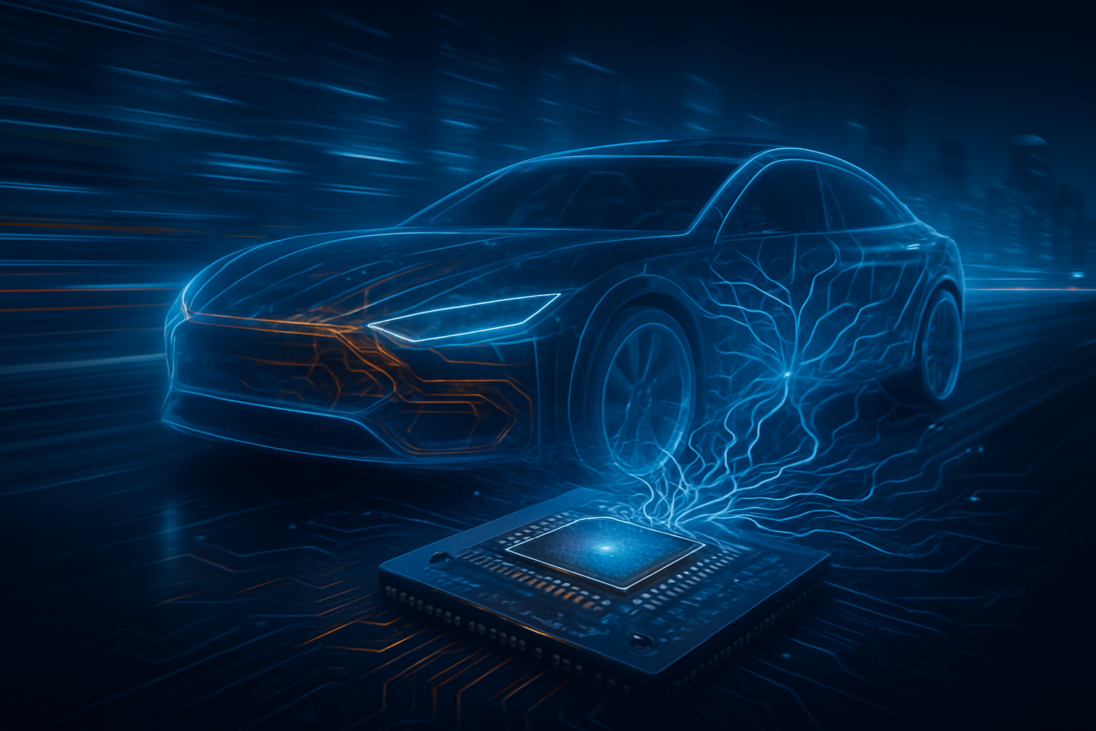
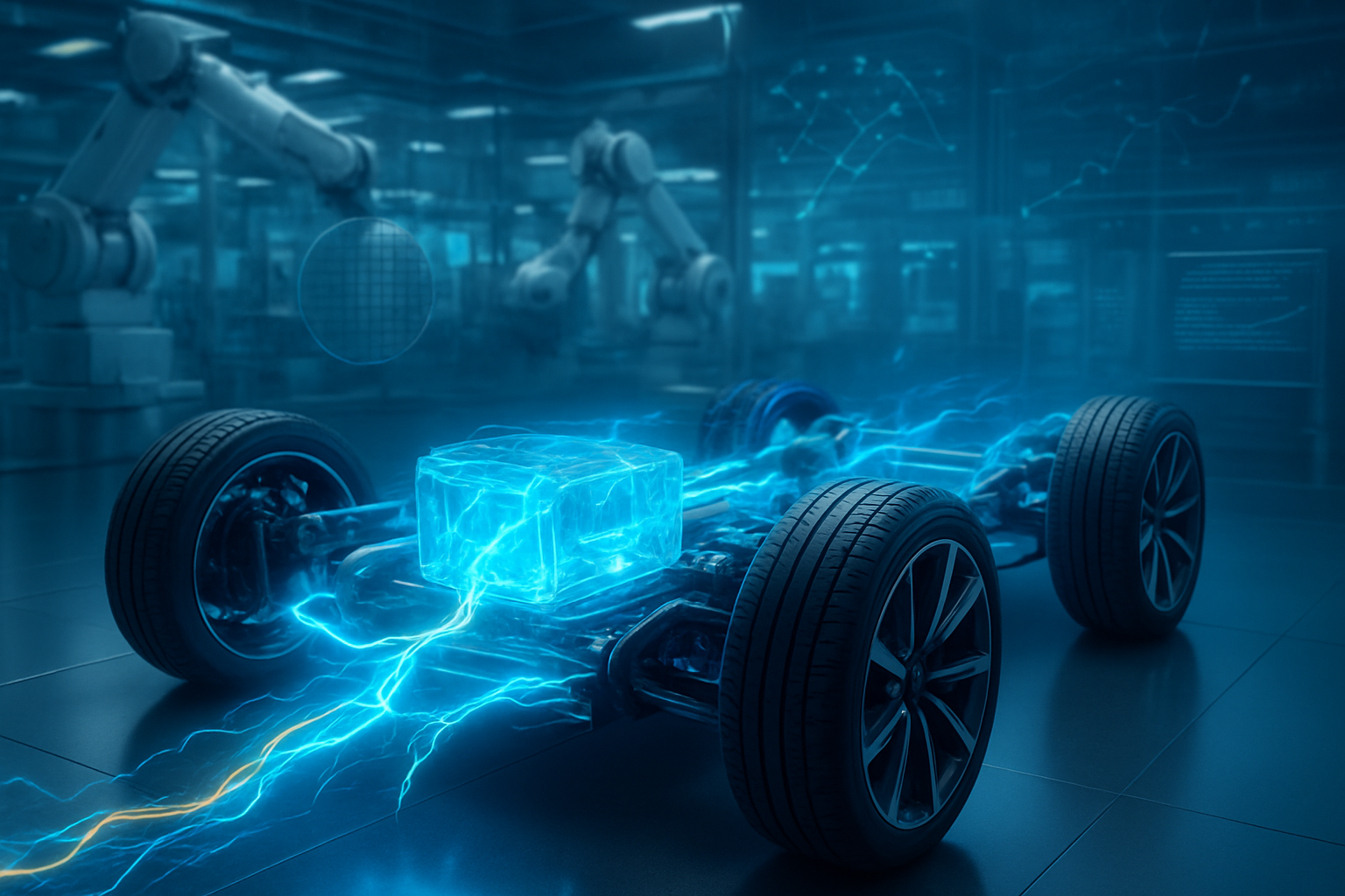
Technically, Silicon Carbide is a "wide-bandgap" (WBG) semiconductor, meaning it can operate at much higher voltages, temperatures, and frequencies than standard silicon. In the context of an EV, this allows for the creation of power inverters—the components that convert battery DC power to motor AC power—that are significantly more efficient. As of early 2026, the latest Generation-3 SiC MOSFETs from STMicroelectronics (NYSE: STM) and the CoolSiC Gen 2 line from Infineon Technologies (FWB: IFX) have achieved powertrain efficiencies exceeding 99%.
This efficiency is not just a laboratory metric; it translates directly to thermal management. Because SiC generates up to 50% less heat during power switching than traditional silicon, the cooling systems in 2026 EVs are roughly 10% lighter and smaller. This creates a vicious cycle of weight reduction: a lighter cooling system allows for a lighter chassis, which in turn increases the vehicle's range. Current data shows that SiC-equipped vehicles are achieving an average 7% range increase over 2023 models without any increase in battery size.
Furthermore, the transition to 200mm wafers has been the industry's "Holy Grail." Previously, most SiC was manufactured on 150mm (6-inch) wafers, which were prone to higher defect rates and lower output. The successful scaling to 200mm in late 2025 has increased usable chips per wafer by nearly 85%. This manufacturing milestone, supported by AI-driven defect detection and predictive fab management, has finally brought the price of SiC modules close to parity with high-end silicon components.
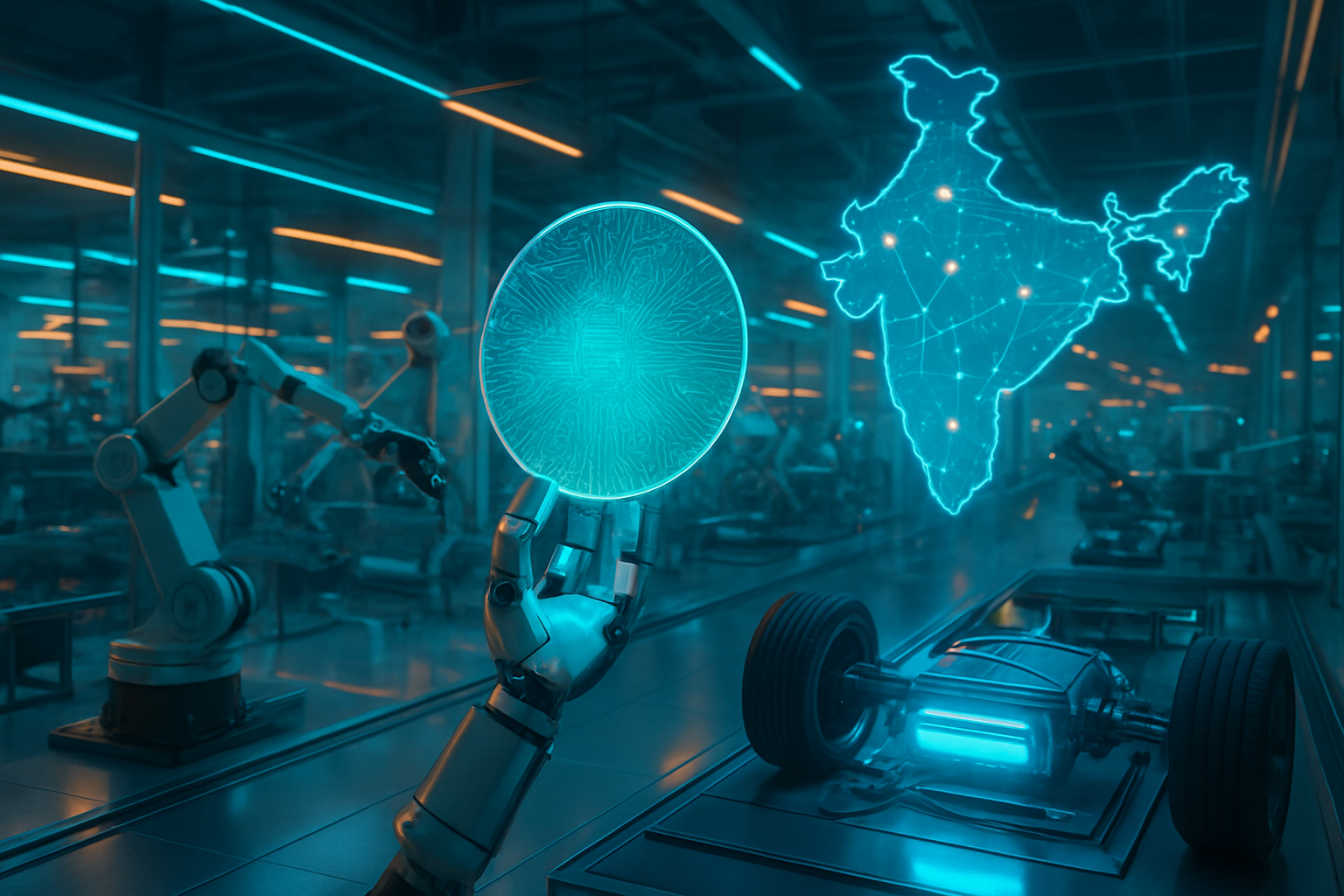
The competitive landscape of 2026 is dominated by a few key players who moved early to secure their supply chains. STMicroelectronics has solidified its lead through a "Silicon Carbide Campus" in Catania, Italy, which handles the entire production cycle from raw powder to finished modules. Their joint venture with Sanan Optoelectronics in China has also reached full capacity, churning out 480,000 wafers annually to meet the insatiable demand of the Chinese EV market. ST’s early partnership with Tesla and recent major deals with Geely and Hyundai have positioned them as the primary backbone of the global EV fleet.
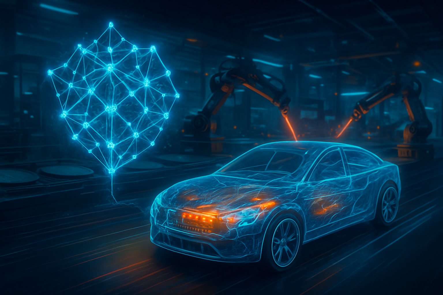
Infineon Technologies has countered with its "One Virtual Fab" strategy, leveraging massive expansions in Villach, Austria, and Kulim, Malaysia. Their recent multi-billion dollar agreement with Stellantis (NYSE: STLA) to standardize power modules across 14 brands has effectively locked out smaller competitors from a significant portion of the European market. Infineon's focus on "CoolSiC" technology has also made them the preferred partner for high-performance entrants like Xiaomi (HKG: 1810), whose latest SU7 models utilize Infineon modules to achieve record-breaking acceleration and charging metrics.
This production surge is causing significant disruption for traditional power semiconductor makers who were late to the SiC transition. Companies that relied on aging silicon-based Insulated-Gate Bipolar Transistors (IGBTs) are finding themselves relegated to the low-end, budget vehicle market. Meanwhile, the strategic advantage has shifted toward vertically integrated companies—those that own everything from the SiC crystal growth to the final module packaging—as they are better insulated from the supply shocks that plagued the industry earlier this decade.
The broader significance of the SiC surge extends far beyond the driveway. This technology is a critical component of the global push for decarbonization and energy independence. As EV adoption accelerates thanks to SiC-enabled charging convenience, the demand for fossil fuels is seeing its most significant decline in history. Moreover, the high-frequency switching capabilities of SiC are being applied to the "Smart Grid," allowing for more efficient integration of renewable energy sources like solar and wind into the national electricity supply.
However, the rapid shift has raised concerns regarding material sourcing. Silicon carbide requires high-purity carbon and silicon, and the manufacturing process is incredibly energy-intensive. There are also geopolitical implications, as the race for SiC dominance has led to "semiconductor nationalism," with the US, EU, and China all vying to subsidize local production hubs. This has mirrored previous milestones in the AI chip race, where control over manufacturing capacity has become a matter of national security.
In terms of market impact, the democratization of 800-volt charging is the most visible breakthrough for the general public. It effectively addresses "range anxiety" and "wait-time anxiety," which were the two largest hurdles for EV adoption in the early 2020s. By early 2026, the infrastructure and the vehicle technology have finally synchronized, creating a user experience that is finally comparable—if not superior—to the traditional gas station model.
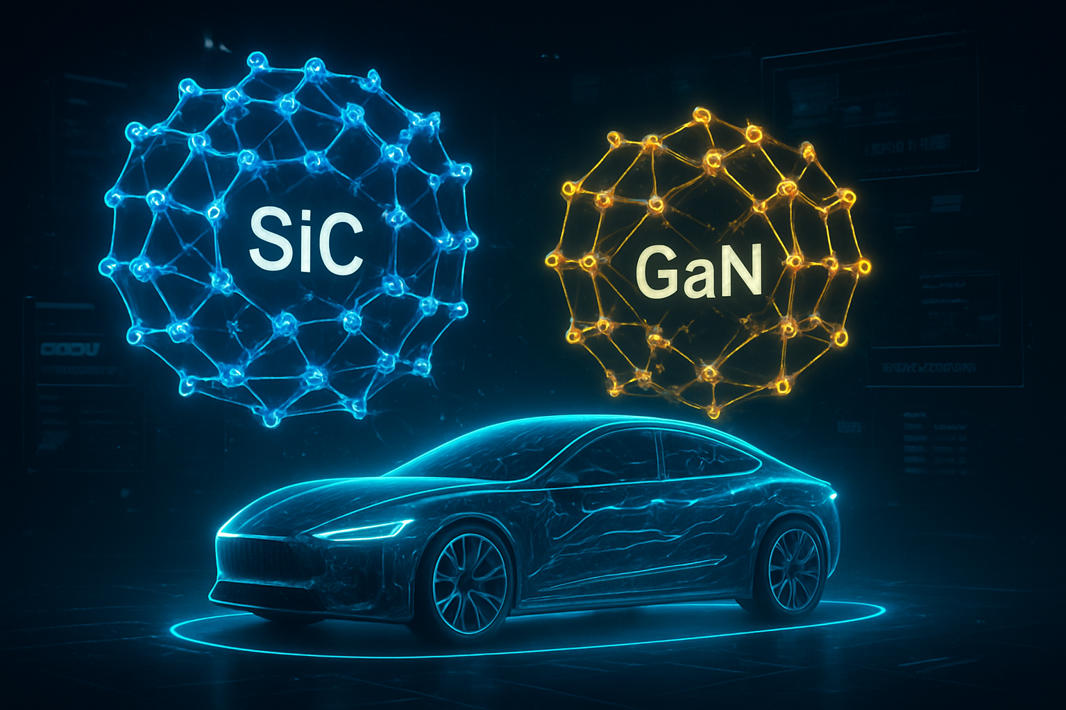
Looking ahead, the next frontier for SiC is the potential transition to 300mm (12-inch) wafers, which would represent another massive leap in production efficiency. While currently in the pilot phase at firms like Infineon, full-scale 300mm production is expected by the late 2020s. We are also beginning to see the integration of SiC with Gallium Nitride (GaN) in "hybrid" power systems, which could lead to even smaller onboard chargers and DC-DC converters for the next generation of software-defined vehicles.
Experts predict that the lessons learned from scaling SiC will be applied to other advanced materials, potentially accelerating the development of solid-state batteries. The primary challenge remaining is the recycling of these advanced power modules. As the first generation of SiC-heavy vehicles reaches the end of its life toward the end of this decade, the industry will need to develop robust methods for recovering and reusing these specialized materials.
The Silicon Carbide revolution of 2026 is more than just an incremental upgrade; it is the fundamental technological shift that has made the electric vehicle a viable reality for the global majority. Through the aggressive scaling efforts of STMicroelectronics and Infineon, the industry has successfully moved past the "prototyping" phase of high-performance electrification and into a high-volume, high-efficiency era.
The key takeaway for 2026 is that the powertrain is no longer a commodity—it is a sophisticated platform for innovation. As we watch the market evolve in the coming months, the focus will likely shift toward software-defined power management, where AI algorithms optimize SiC switching in real-time to squeeze every possible kilometer out of the battery. For now, the "SiC Surge" stands as one of the most significant engineering triumphs of the mid-2020s, forever changing how the world moves.
This content is intended for informational purposes only and represents analysis of current AI and semiconductor developments.
TokenRing AI delivers enterprise-grade solutions for multi-agent AI workflow orchestration, AI-powered development tools, and seamless remote collaboration platforms.
For more information, visit https://www.tokenring.ai/.