Tag: Silicon Chips

  • Lighting Up the AI Supercycle: Silicon Photonics and the End of the Copper Era

    Lighting Up the AI Supercycle: Silicon Photonics and the End of the Copper Era

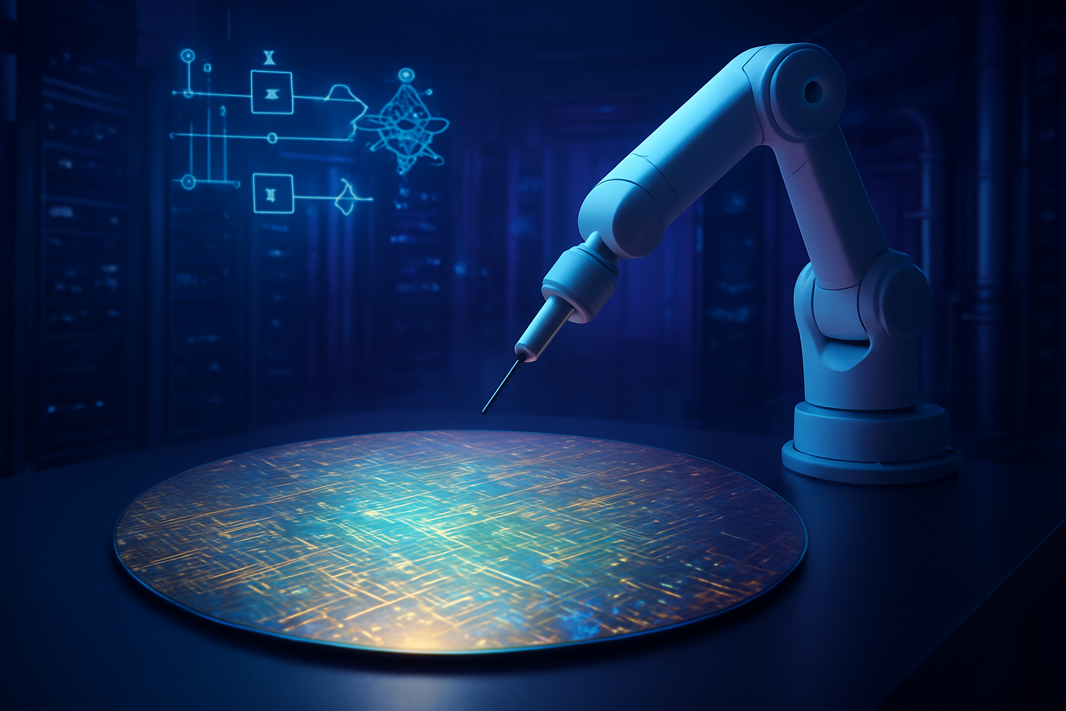
    As the global race for Artificial General Intelligence (AGI) accelerates, the infrastructure supporting these massive models has hit a physical "Copper Wall." Traditional electrical interconnects, which have long served as the nervous system of the data center, are struggling to keep pace with the staggering bandwidth requirements and power consumption of next-generation AI clusters. In response, a fundamental shift is underway: the "Photonic Pivot." By early 2026, the transition from electricity to light for data transfer has become the defining technological breakthrough of the decade, enabling the construction of "Gigascale AI Factories" that were previously thought to be physically impossible.

    Silicon photonics—the integration of laser-generated light and silicon-based electronics on a single chip—is no longer a laboratory curiosity. With the recent mass deployment of 1.6 Terabit (1.6T) optical transceivers and the emergence of Co-Packaged Optics (CPO), the industry is witnessing a revolutionary leap in efficiency. This shift is not merely about speed; it is about survival. As data centers consume an ever-increasing share of the world's electricity, the ability to move data using photons instead of electrons offers a path toward a sustainable AI future, reducing interconnect power consumption by as much as 70% while providing a ten-fold increase in bandwidth density.

    The Technical Foundations: Breaking Through the Copper Wall

    The fundamental problem with electricity in 2026 is resistance. As signal speeds push toward 448G per lane, the heat generated by pushing electrons through copper wires becomes unmanageable, and signal integrity degrades over just a few centimeters. To solve this, the industry has turned to Co-Packaged Optics (CPO). Unlike traditional pluggable optics that sit at the edge of a server chassis, CPO integrates the optical engine directly onto the GPU or switch package. This allows for a "Photonic Integrated Circuit" (PIC) to reside just millimeters away from the processing cores, virtually eliminating the energy-heavy electrical path required by older architectures.

    Leading the charge is Taiwan Semiconductor Manufacturing Company (NYSE:TSM) with its COUPE (Compact Universal Photonic Engine) platform. Entering mass production in late 2025, COUPE utilizes SoIC-X (System on Integrated Chips) technology to stack electrical dies directly on top of photonic dies using 3D packaging. This architecture enables bandwidth densities exceeding 2.5 Tbps/mm—a 12.5-fold increase over 2024-era copper solutions. Furthermore, the energy-per-bit has plummeted to below 5 picojoules per bit (pJ/bit), compared to the 15-30 pJ/bit required by traditional digital signal processing (DSP)-based pluggables just two years ago.

    The shift is further supported by the Optical Internetworking Forum (OIF) and its CEI-448G framework, which has standardized the move to PAM6 and PAM8 modulation. These standards are the blueprint for the 3.2T and 6.4T modules currently sampling for 2027 deployment. By moving the light source outside the package through the External Laser Source Form Factor (ELSFP), engineers have also found a way to manage the intense heat of high-power lasers, ensuring that the silicon photonics engines can operate at peak performance without self-destructing under the thermal load of a modern AI workload.

    A New Hierarchy: Market Dynamics and Industry Leaders

    The emergence of silicon photonics has fundamentally reshaped the competitive landscape of the semiconductor industry. NVIDIA (NASDAQ:NVDA) recently solidified its dominance with the launch of the Rubin architecture at CES 2026. Rubin is the first GPU platform designed from the ground up to utilize "Ethernet Photonics" MCM packages, linking millions of cores into a single cohesive "Super-GPU." By integrating silicon photonic engines directly into its SN6800 switches, NVIDIA has achieved a 5x reduction in power consumption per port, effectively decoupling the growth of AI performance from the growth of energy costs.

    Meanwhile, Broadcom (NASDAQ:AVGO) has maintained its lead in the networking sector with the Tomahawk 6 "Davisson" switch. Announced in late 2025, this 102.4 Tbps Ethernet switch leverages CPO to eliminate nearly 1,000 watts of heat from the front panel of a single rack unit. This energy saving is critical for the shift to high-density liquid cooling, which has become mandatory for 2026-class AI data centers. Not to be outdone, Intel (NASDAQ:INTC) is leveraging its 18A process node to produce Optical Compute Interconnect (OCI) chiplets. These chiplets support transmission distances of up to 100 meters, enabling a "disaggregated" data center design where compute and memory pools are physically separated but linked by near-instantaneous optical connections.

    The startup ecosystem is also seeing massive consolidation and valuation surges. Early in 2026, Marvell Technology (NASDAQ:MRVL) completed the acquisition of startup Celestial AI in a deal valued at over $5 billion. Celestial’s "Photonic Fabric" technology allows processors to access shared memory at HBM (High Bandwidth Memory) speeds across entire server racks. Similarly, Lightmatter and Ayar Labs have reached multi-billion dollar "unicorn" status, providing critical 3D-stacked photonic superchips and in-package optical I/O to a hungry market.

    The Broader Landscape: Sustainability and the Scaling Limit

    The significance of silicon photonics extends far beyond the bottom lines of chip manufacturers; it is a critical component of global energy policy. In 2024 and 2025, the exponential growth of AI led to concerns that data center energy consumption would outstrip the capacity of regional power grids. Silicon photonics provides a pressure release valve. By reducing the interconnect power—which previously accounted for nearly 30% of a cluster's total energy draw—down to less than 10%, the industry can continue to scale AI models without requiring the construction of a dedicated nuclear power plant for every new "Gigascale" facility.

    However, this transition has also created a new digital divide. The extreme complexity and cost of 2026-era silicon photonics mean that the most advanced AI capabilities are increasingly concentrated in the hands of "Hyperscalers" and elite labs. While companies like Microsoft (NASDAQ:MSFT) and Google have the capital to invest in CPO-ready infrastructure, smaller AI startups are finding themselves priced out, forced to rely on older, less efficient copper-based hardware. This concentration of "optical compute power" may have long-term implications for the democratization of AI.

    Furthermore, the transition has not been without its technical hurdles. Manufacturing yields for CPO remain lower than traditional semiconductors due to the extreme precision required for optical fiber alignment. "Optical loss" localization remains a challenge for quality control, where a single microscopic defect in a waveguide can render an entire multi-thousand-dollar GPU package unusable. These "post-packaging failures" have kept the cost of photonic-enabled hardware high, even as performance metrics soar.

    The Road to 2030: Optical Computing and Beyond

    Looking toward the late 2020s, the current breakthroughs in optical interconnects are expected to evolve into true "Optical Computing." Startups like Neurophos—recently backed by a $110 million Series A round led by Microsoft (NASDAQ:MSFT)—are working on Optical Processing Units (OPUs) that use light not just to move data, but to process it. These devices leverage the properties of light to perform the matrix-vector multiplications central to AI inference with almost zero energy consumption.

    In the near term, the industry is preparing for the 6.4T and 12.8T eras. We expect to see the wider adoption of Quantum Dot (QD) lasers, which offer greater thermal stability than the Indium Phosphide lasers currently in use. Challenges remain in the realm of standardized "pluggable" light sources, as the industry debates the best way to make these complex systems interchangeable across different vendors. Most experts predict that by 2028, the "Copper Wall" will be a distant memory, with optical fabrics becoming the standard for every level of the compute stack, from rack-to-rack down to chip-to-chip communication.

    A New Era for Intelligence

    The "Photonic Pivot" of 2026 marks a turning point in the history of computing. By overcoming the physical limitations of electricity, silicon photonics has cleared the path for the next generation of AI models, which will likely reach the scale of hundreds of trillions of parameters. The ability to move data at the speed of light, with minimal heat and energy loss, is the key that has unlocked the current AI supercycle.

    As we look ahead, the success of this transition will depend on the industry's ability to solve the yield and reliability challenges that currently plague CPO manufacturing. Investors and tech enthusiasts should keep a close eye on the rollout of 3.2T modules in the second half of 2026 and the progress of TSMC's COUPE platform. For now, one thing is certain: the future of AI is bright, and it is powered by light.


    This content is intended for informational purposes only and represents analysis of current AI developments.

    TokenRing AI delivers enterprise-grade solutions for multi-agent AI workflow orchestration, AI-powered development tools, and seamless remote collaboration platforms.
    For more information, visit https://www.tokenring.ai/.

  • The Silicon Renaissance: How CMOS Manufacturing is Solving the Quantum Scaling Crisis

    The Silicon Renaissance: How CMOS Manufacturing is Solving the Quantum Scaling Crisis

    As 2025 draws to a close, the quantum computing landscape has reached a historic inflection point. Long dominated by exotic architectures like superconducting loops and trapped ions, the industry is witnessing a decisive shift toward silicon-based spin qubits. In a series of breakthrough announcements this month, researchers and industrial giants have demonstrated that the path to a million-qubit quantum computer likely runs through the same 300mm silicon wafer foundries that powered the digital revolution.

    The immediate significance of this shift cannot be overstated. By leveraging existing Complementary Metal-Oxide-Semiconductor (CMOS) manufacturing techniques, the quantum industry is effectively "piggybacking" on trillions of dollars of historical investment in semiconductor fabrication. This month's data suggests that the "utility-scale" era of quantum computing is no longer a theoretical projection but a manufacturing reality, as silicon chips begin to offer the high fidelities and industrial reproducibility required for fault-tolerant operations.

    Industrializing the Qubit: 99.99% Fidelity and 300mm Scaling

    The most striking technical achievement of December 2025 came from Silicon Quantum Computing (SQC), which published results in Nature demonstrating a multi-register processor with a staggering 99.99% gate fidelity. Unlike previous "hero" devices that lost performance as they grew, SQC’s architecture showed that qubit quality actually strengthens as the system scales. This breakthrough is complemented by Diraq, which, in collaboration with the research hub imec, proved that high-fidelity qubits could be mass-produced. They reported that qubits randomly selected from a standard 300mm industrial wafer achieved over 99% two-qubit fidelity, a milestone that signals the end of hand-crafted quantum processors.

    Technically, these silicon spin qubits function by trapping single electrons in "quantum dots" defined within a silicon layer. The 2025 breakthroughs have largely focused on the integration of cryo-CMOS control electronics. Historically, quantum chips were limited by the "wiring nightmare"—thousands of coaxial cables required to connect qubits at millikelvin temperatures to room-temperature controllers. New "monolithic" designs now place the control transistors directly on the same silicon footprint as the qubits. This is made possible by the development of low-power cryo-CMOS transistors, such as those from European startup SemiQon, which reduce power consumption by 100x, preventing the delicate quantum state from being disrupted by heat.

    This approach differs fundamentally from the superconducting qubits favored by early pioneers. While superconducting systems are physically large—often the size of a thumbnail for a single qubit—silicon spin qubits are roughly the size of a standard transistor (about 100 nanometers). This allows for a density of millions of qubits per square centimeter, mirroring the scaling trajectory of classical microprocessors. The initial reaction from the research community has been one of "cautious triumph," with experts noting that the transition to 300mm wafers solves the reproducibility crisis that has plagued quantum hardware for a decade.

    The Foundry Model: Intel and IBM Pivot to Silicon Scale

    The move toward silicon-based quantum computing has massive implications for the semiconductor titans. Intel Corp (NASDAQ: INTC) has emerged as a frontrunner by aligning its quantum roadmap with its most advanced logic nodes. In late 2025, Intel’s 18A (1.8nm equivalent) process entered mass production, featuring RibbonFET (gate-all-around) architecture. Intel is now adapting these GAA transistors to act as quantum dots, essentially treating a qubit as a specialized transistor. By using standard Extreme Ultraviolet (EUV) lithography, Intel can define qubit arrays with a precision and uniformity that smaller startups cannot match.

    Meanwhile, International Business Machines Corp (NYSE: IBM), though traditionally a champion of superconducting qubits, has made a strategic pivot toward silicon-style manufacturing efficiencies. In November 2025, IBM unveiled its Nighthawk processor, which officially shifted its fabrication to 300mm facilities. This move has allowed IBM to increase the physical complexity of its chips by 10x while maintaining the low error rates needed for its "Quantum Loon" error-correction architecture. The competitive landscape is shifting from "who has the best qubit" to "who can manufacture the most qubits at scale," favoring companies with deep ties to major foundries.

    Foundries like GlobalFoundries Inc (NASDAQ: GFS) and Taiwan Semiconductor Manufacturing Company (NYSE: TSM) are positioning themselves as the essential "factories" for the quantum ecosystem. GlobalFoundries’ 22FDX process has become a gold standard for spin qubits, as seen in the recent "Bloomsbury" chip which features over 1,000 integrated quantum dots. For TSMC, the opportunity lies in advanced packaging; their CoWoS (Chip-on-Wafer-on-Substrate) technology is now being used to stack classical AI processors directly on top of quantum chips, enabling the low-latency error decoding required for real-time quantum calculations.

    Geopolitics and the "Wiring Nightmare" Breakthrough

    The wider significance of silicon-based quantum computing extends into energy efficiency and global supply chains. One of the primary concerns with scaling quantum computers has been the massive energy required to cool the systems. However, the 2025 breakthroughs in cryo-CMOS mean that more of the control logic happens inside the dilution refrigerator, reducing the thermal load and the physical footprint of the machine. This makes quantum data centers a more realistic prospect for the late 2020s, potentially fitting into existing server rack architectures rather than requiring dedicated warehouses.

    There is also a significant geopolitical dimension to the silicon shift. High-performance spin qubits require isotopically pure silicon-28, a material that was once difficult to source. The industrialization of Si-28 production in 2024 and 2025 has created a new high-tech commodity market. Much like the race for lithium or cobalt, the ability to produce and refine "quantum-grade" silicon is becoming a matter of national security for technological superpowers. This mirrors previous milestones in the AI landscape, such as the rush for H100 GPUs, where the hardware substrate became the ultimate bottleneck for progress.

    However, the rapid move toward CMOS-based quantum chips has raised concerns about the "quantum divide." As the manufacturing requirements shift toward multi-billion dollar 300mm fabs, smaller research institutions and startups may find themselves priced out of the hardware game, forced to rely on cloud access provided by the few giants—Intel, IBM, and the major foundries—who control the means of production.

    The Road to Fault Tolerance: What’s Next for 2026?

    Looking ahead, the next 12 to 24 months will likely focus on the transition from "noisy" qubits to logical qubits. While we now have the ability to manufacture thousands of physical qubits on a single chip, several hundred physical qubits are needed to form one error-corrected "logical" qubit. Experts predict that 2026 will see the first demonstration of a "logical processor" where multiple logical qubits perform a complex algorithm with higher fidelity than their underlying physical components.

    Potential applications on the near horizon include high-precision material science and drug discovery. With the density provided by silicon chips, we are approaching the threshold where quantum computers can simulate the molecular dynamics of nitrogen fixation or carbon capture more accurately than any classical supercomputer. The challenge remains in the software stack—developing compilers that can efficiently map these algorithms onto the specific topologies of silicon spin qubit arrays.

    In the long term, the integration of quantum and classical processing on a single "Quantum SoC" (System on a Chip) is the ultimate goal. Experts from Diraq and Intel suggest that by 2028, we could see chips containing millions of qubits, finally reaching the scale required to break current RSA encryption or revolutionize financial modeling.

    A New Chapter in the Quantum Race

    The breakthroughs of late 2025 have solidified silicon's position as the most viable substrate for the future of quantum computing. By proving that 99.99% fidelity is achievable on 300mm wafers, the industry has bridged the gap between laboratory curiosity and industrial product. The significance of this development in AI and computing history cannot be understated; it represents the moment quantum computing stopped trying to reinvent the wheel and started using the most sophisticated wheel ever created: the silicon transistor.

    As we move into 2026, the key metrics to watch will be the "logical qubit count" and the continued integration of cryo-CMOS electronics. The race is no longer just about quantum physics—it is about the mastery of the semiconductor supply chain. For the tech industry, the message is clear: the quantum future will be built on a silicon foundation.


    This content is intended for informational purposes only and represents analysis of current AI and quantum developments.

    TokenRing AI delivers enterprise-grade solutions for multi-agent AI workflow orchestration, AI-powered development tools, and seamless remote collaboration platforms.
    For more information, visit https://www.tokenring.ai/.