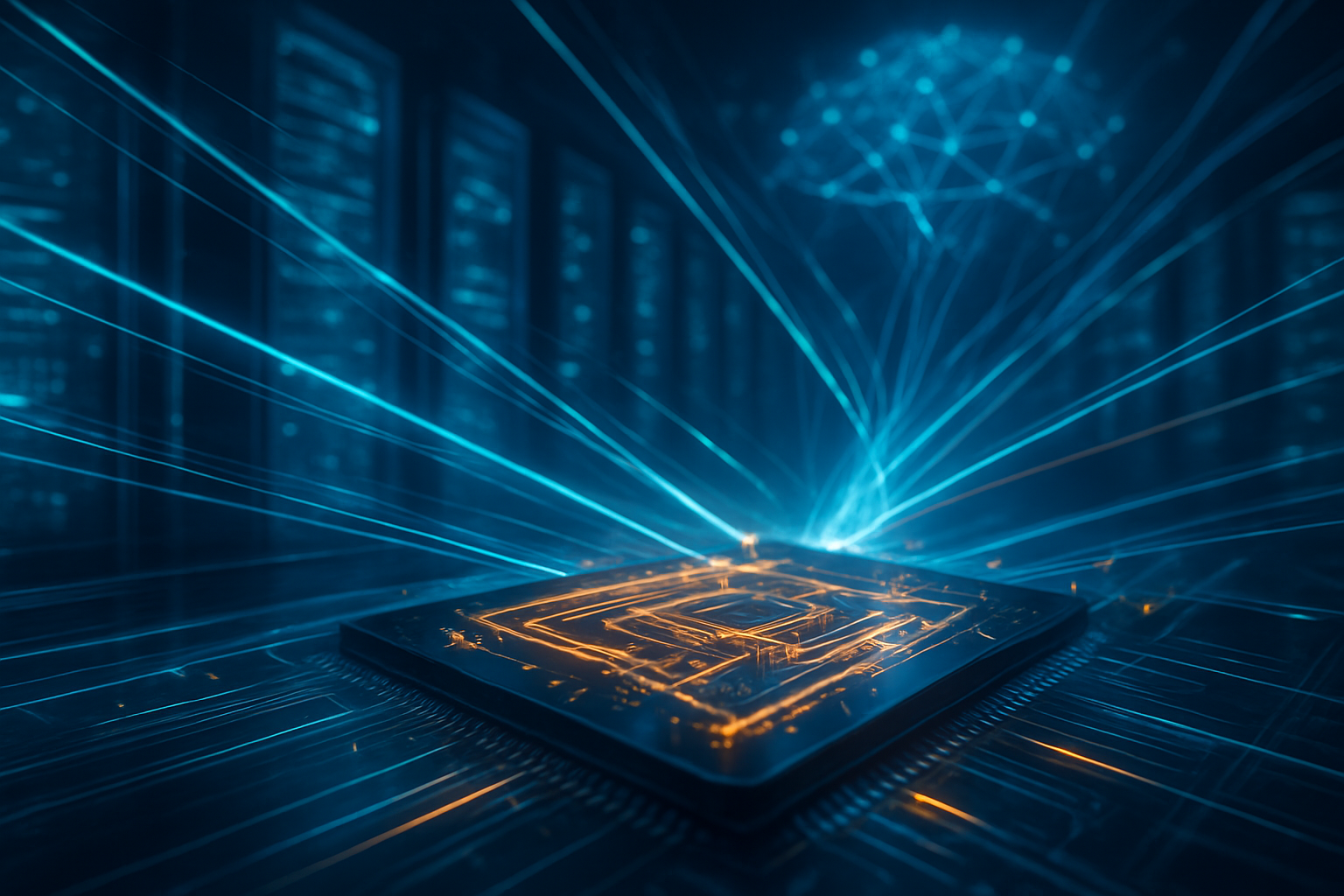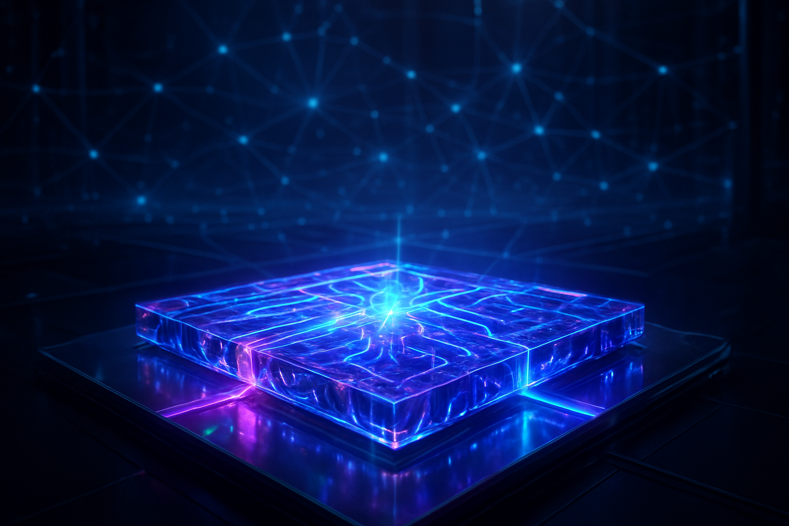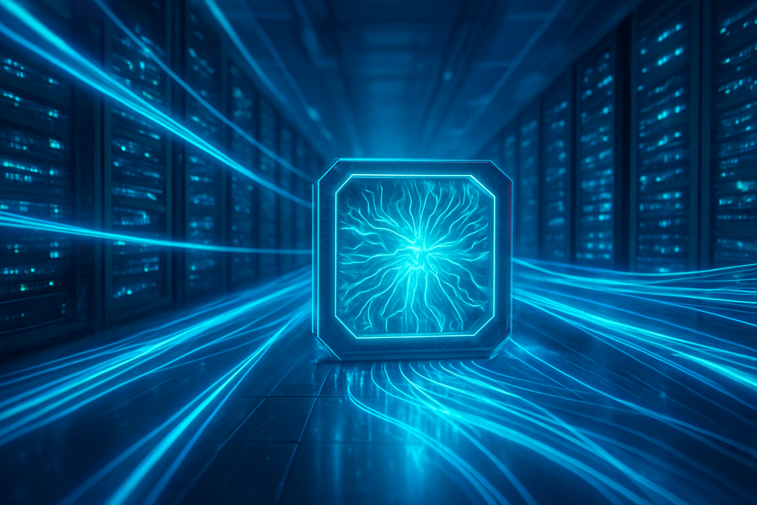
As of January 2026, the artificial intelligence industry has reached a pivotal infrastructure milestone: the definitive transition from copper-based electrical interconnects to light-based communication. For years, the "Copper Wall"—the physical limit at which electrical signals traveling through metal wires become too hot and inefficient to scale—threatened to stall the growth of massive AI models. Today, that wall has been dismantled. The shift toward Optical I/O (Input/Output) and Photonic Integrated Circuits (PICs) is no longer a future-looking experimental venture; it has become the mandatory standard for the world's most advanced data centers.
By replacing traditional electricity with light for chip-to-chip communication, the industry has successfully decoupled bandwidth growth from energy consumption. This transformation is currently enabling the deployment of "Million-GPU" clusters that would have been thermally and electrically impossible just two years ago. As the infrastructure for 2026 matures, Silicon Photonics has emerged as the primary solution to the AI data center energy crisis, reducing the power required for data movement by over 70% and fundamentally changing how supercomputers are built.
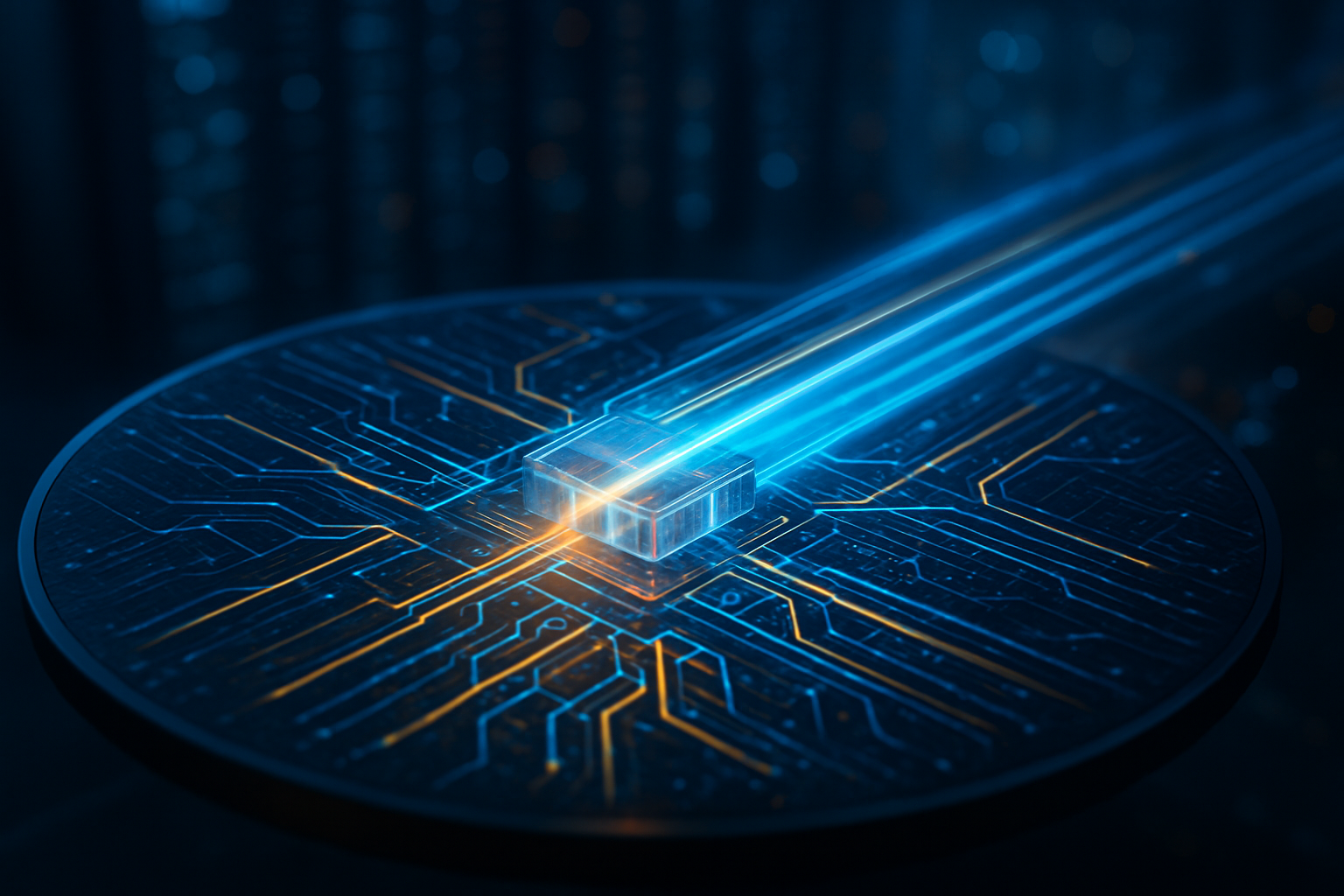
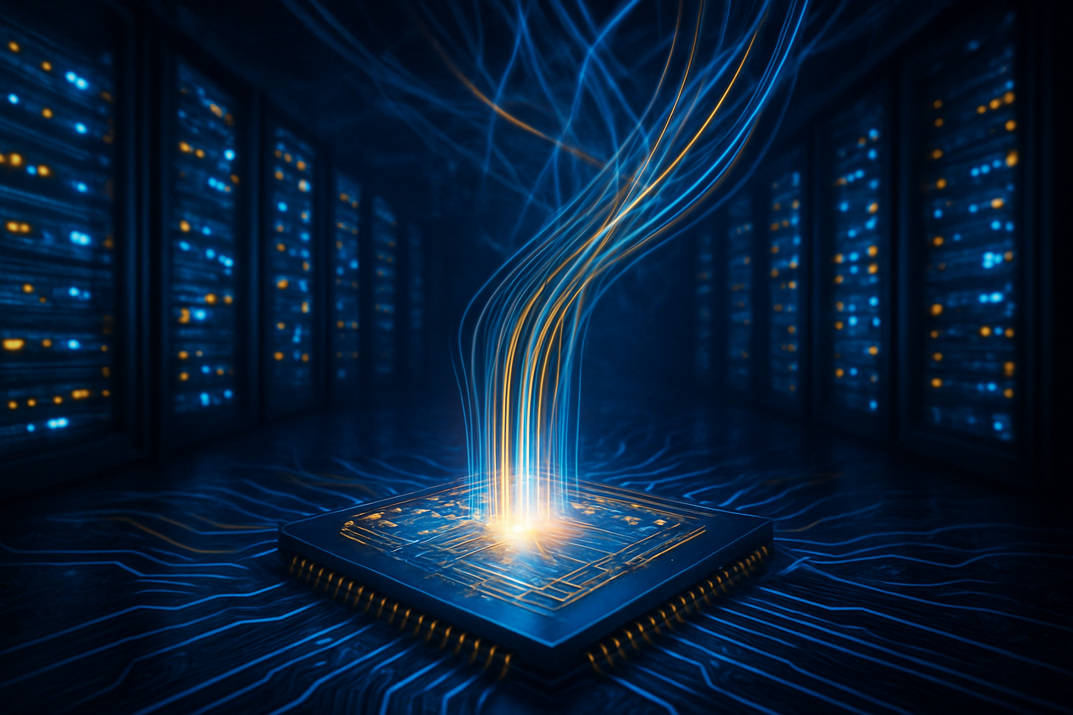
The technical shift driving this revolution centers on Co-Packaged Optics (CPO) and the arrival of 1.6 Terabit (1.6T) optical modules as the new industry backbone. In the previous era, data moved between processors via copper traces on circuit boards, which generated immense heat due to electrical resistance. In 2026, companies like NVIDIA (NASDAQ: NVDA) and Broadcom (NASDAQ: AVGO) are shipping systems where optical engines are integrated directly onto the chip package. This allows data to be converted into light pulses immediately at the "shoreline" of the processor, traveling through fiber optics with almost zero resistance or signal degradation.
Current specifications for 2026-era optical I/O are staggering compared to the benchmarks of 2024. While traditional electrical interconnects consumed roughly 15 to 20 picojoules per bit (pJ/bit), current Photonic Integrated Circuits have pushed this efficiency to below 5 pJ/bit. Furthermore, the bandwidth density has skyrocketed; while copper was limited to approximately 200 Gbps per millimeter of chip edge, optical I/O now supports over 2.5 Tbps per millimeter. This allows for massive throughput without the massive footprint. The integration of Thin-Film Lithium Niobate (TFLN) modulators has further enabled these speeds, offering bandwidths exceeding 110 GHz at drive voltages lower than 1V.
The initial reaction from the AI research community has been one of relief. Experts at leading labs had warned that power constraints would force a "compute plateau" by 2026. However, the successful scaling of optical interconnects has allowed the scaling laws of large language models to continue unabated. By moving the optical engine inside the package—a feat of heterogeneous integration led by Intel (NASDAQ: INTC) and its Optical Compute Interconnect (OCI) chiplets—the industry has solved the "I/O bottleneck" that previously throttled GPU performance during large-scale training runs.
This shift has reshaped the competitive landscape for tech giants and silicon manufacturers alike. NVIDIA (NASDAQ: NVDA) has solidified its dominance with the full-scale production of its Rubin GPU architecture, which utilizes the Quantum-X800 CPO InfiniBand platform. By integrating optical interfaces directly into its switches and GPUs, NVIDIA has dropped per-port power consumption from 30W to just 9W, a strategic advantage that makes its hardware the most energy-efficient choice for hyperscalers like Microsoft (NASDAQ: MSFT) and Google.
Meanwhile, Broadcom (NASDAQ: AVGO) has emerged as a critical gatekeeper of the optical era. Its "Davisson" Tomahawk 6 switch, built using TSMC (NYSE: TSM) Compact Universal Photonic Engine (COUPE) technology, has become the default networking fabric for Tier-1 AI clusters. This has placed immense pressure on legacy networking providers who failed to pivot toward photonics quickly enough. For startups like Lightmatter and Ayar Labs, 2026 represents a "graduation" year; their once-niche optical chiplets and laser sources are now being integrated into custom ASICs for nearly every major cloud provider.
The strategic advantage of adopting PICs is now a matter of economic survival. Companies that can operate data centers with 70% less interconnect power can afford to scale their compute capacity significantly faster than those tethered to copper. This has led to a market "supercycle" where 1.6T optical module shipments are projected to reach 20 million units by the end of the year. The competitive focus has shifted from "who has the fastest chip" to "who can move the most data with the least heat."
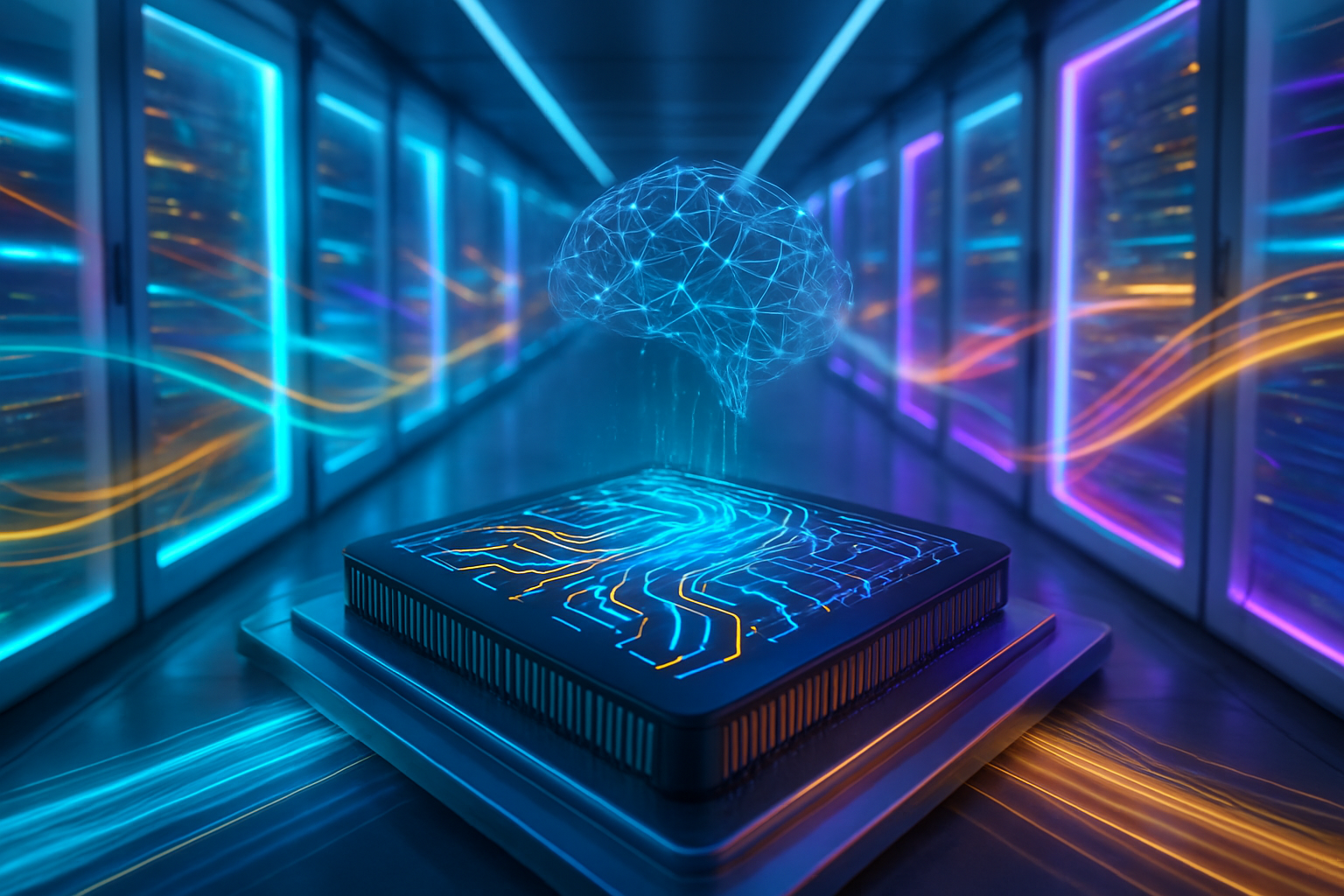
The wider significance of the transition to Silicon Photonics cannot be overstated. It marks a fundamental shift in the physics of computing. For decades, the industry followed Moore’s Law by shrinking transistors, but the energy cost of moving data between those transistors was often ignored. In 2026, the data center has become the "computer," and the optical interconnect is its nervous system. This transition is a critical component of global sustainability efforts, as AI energy demands had previously been projected to consume an unsustainable percentage of the world's power grid.
Comparisons are already being made to the introduction of the transistor itself or the shift from vacuum tubes to silicon. Just as those milestones allowed for the miniaturization of logic, photonics allows for the "extension" of logic across thousands of nodes with near-zero latency. This effectively turns a massive data center into a single, coherent supercomputer. However, this breakthrough also brings concerns regarding the complexity of manufacturing. The precision required to align fiber optics with silicon at a sub-micron scale is immense, leading to a new hierarchy in the semiconductor supply chain where specialized packaging firms hold significant power.
Furthermore, this development has geopolitical implications. As optical I/O becomes the standard, the ability to manufacture advanced PICs has become a national security priority. The reliance on specialized materials like Thin-Film Lithium Niobate and the advanced packaging facilities of TSMC (NYSE: TSM) has created new chokepoints in the global AI race, prompting increased government investment in domestic photonics manufacturing in the US and Europe.
Looking ahead, the roadmap for Silicon Photonics suggests that the current 1.6T standard is only the beginning. Research into 3.2T and 6.4T modules is already well underway, with expectations for commercial deployment by late 2027. Experts predict the next frontier will be "Plasmonic Modulators"—devices 100 times smaller than current photonic components—which could allow optical I/O to be placed not just at the edge of a chip, but directly on top of the compute logic in a 3D-stacked configuration.
Potential applications extend beyond just data centers. On the horizon, we are seeing the first prototypes of "Optical Compute," where light is used not just to move data, but to perform the mathematical calculations themselves. If successful, this could lead to another order-of-magnitude leap in AI efficiency. However, challenges remain, particularly in the longevity of the laser sources used to drive these optical engines. Improving the reliability and "mean time between failures" for these lasers is a top priority for researchers in 2026.
The transition to Optical I/O and Photonic Integrated Circuits represents the most significant architectural shift in data center history since the move to liquid cooling. By using light to solve the energy crisis, the industry has bypassed the physical limitations of electricity, ensuring that the AI revolution can continue its rapid expansion. The key takeaway of early 2026 is clear: the future of AI is no longer just silicon and electrons—it is silicon and photons.
As we move further into the year, the industry will be watching for the first "Million-GPU" deployments to go fully online. These massive clusters will serve as the ultimate proving ground for the reliability and scalability of Silicon Photonics. For investors and tech enthusiasts alike, the "Optical Supercycle" is the defining trend of the 2026 technology landscape, marking the moment when light finally replaced copper as the lifeblood of global intelligence.
This content is intended for informational purposes only and represents analysis of current AI developments.
TokenRing AI delivers enterprise-grade solutions for multi-agent AI workflow orchestration, AI-powered development tools, and seamless remote collaboration platforms.
For more information, visit https://www.tokenring.ai/.