Tag: Silicon Photonics

  • Breaking the Copper Wall: The Dawn of the Optical Era in AI Computing

    Breaking the Copper Wall: The Dawn of the Optical Era in AI Computing

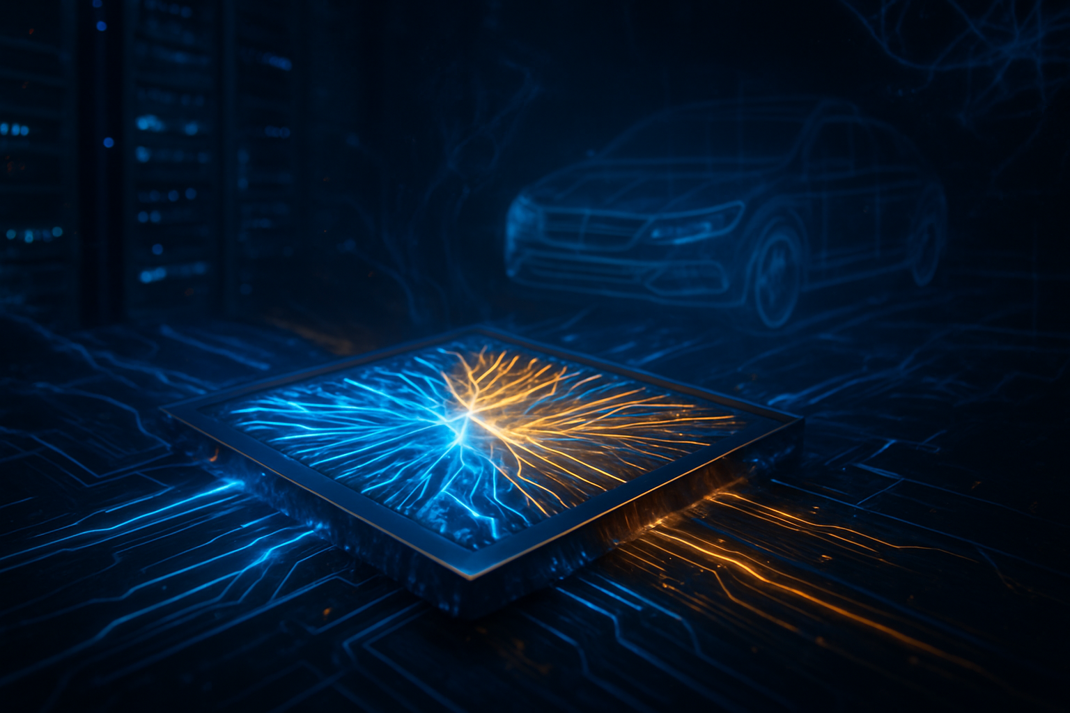
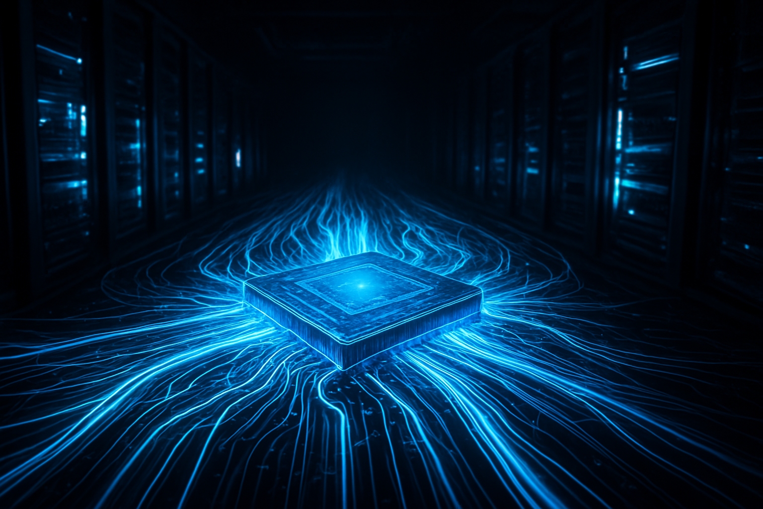
    As of January 2026, the artificial intelligence industry has reached a pivotal architectural milestone dubbed the "Transition to the Era of Light." For decades, the movement of data between chips relied on copper wiring, but as AI models scaled to trillions of parameters, the industry hit a physical limit known as the "Copper Wall." At signaling speeds of 224 Gbps, traditional copper interconnects began consuming nearly 30% of total cluster power, with signal degradation so severe that reach was limited to less than a single meter without massive, heat-generating amplification.

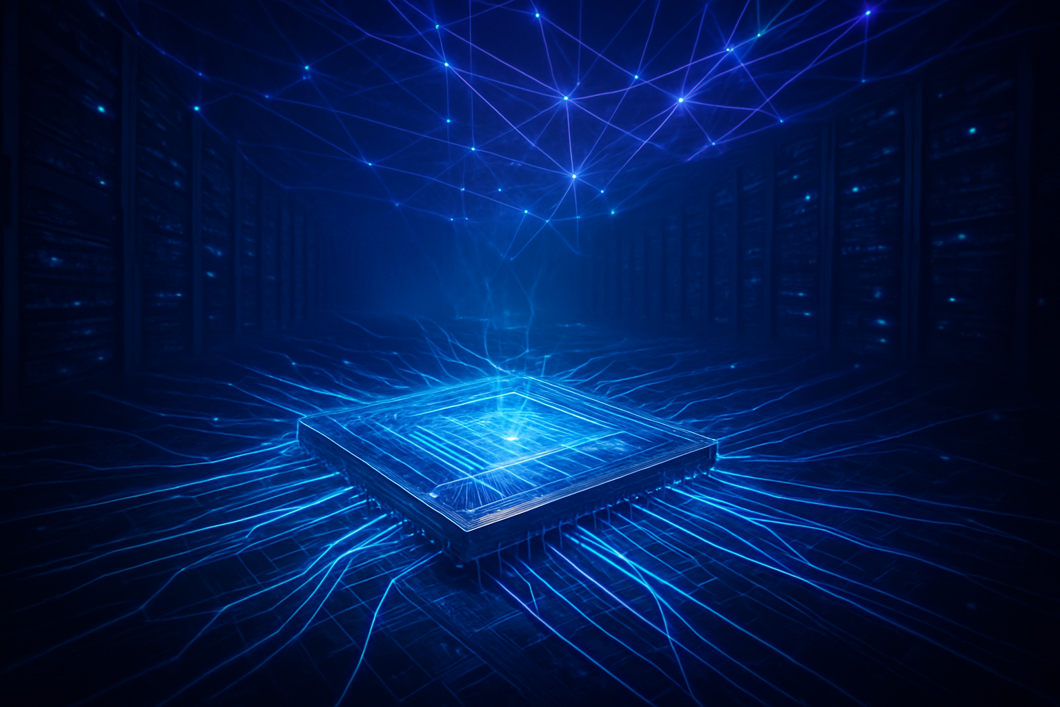
    This month, the shift to Silicon Photonics (SiPh) and Co-Packaged Optics (CPO) has officially moved from experimental labs to the heart of the world’s most powerful AI clusters. By replacing electrical signals with laser-driven light, the industry is drastically reducing latency and power consumption, enabling the first "million-GPU" clusters required for the next generation of Artificial General Intelligence (AGI). This leap forward represents the most significant change in computer architecture since the introduction of the transistor, effectively decoupling AI scaling from the physical constraints of electricity.

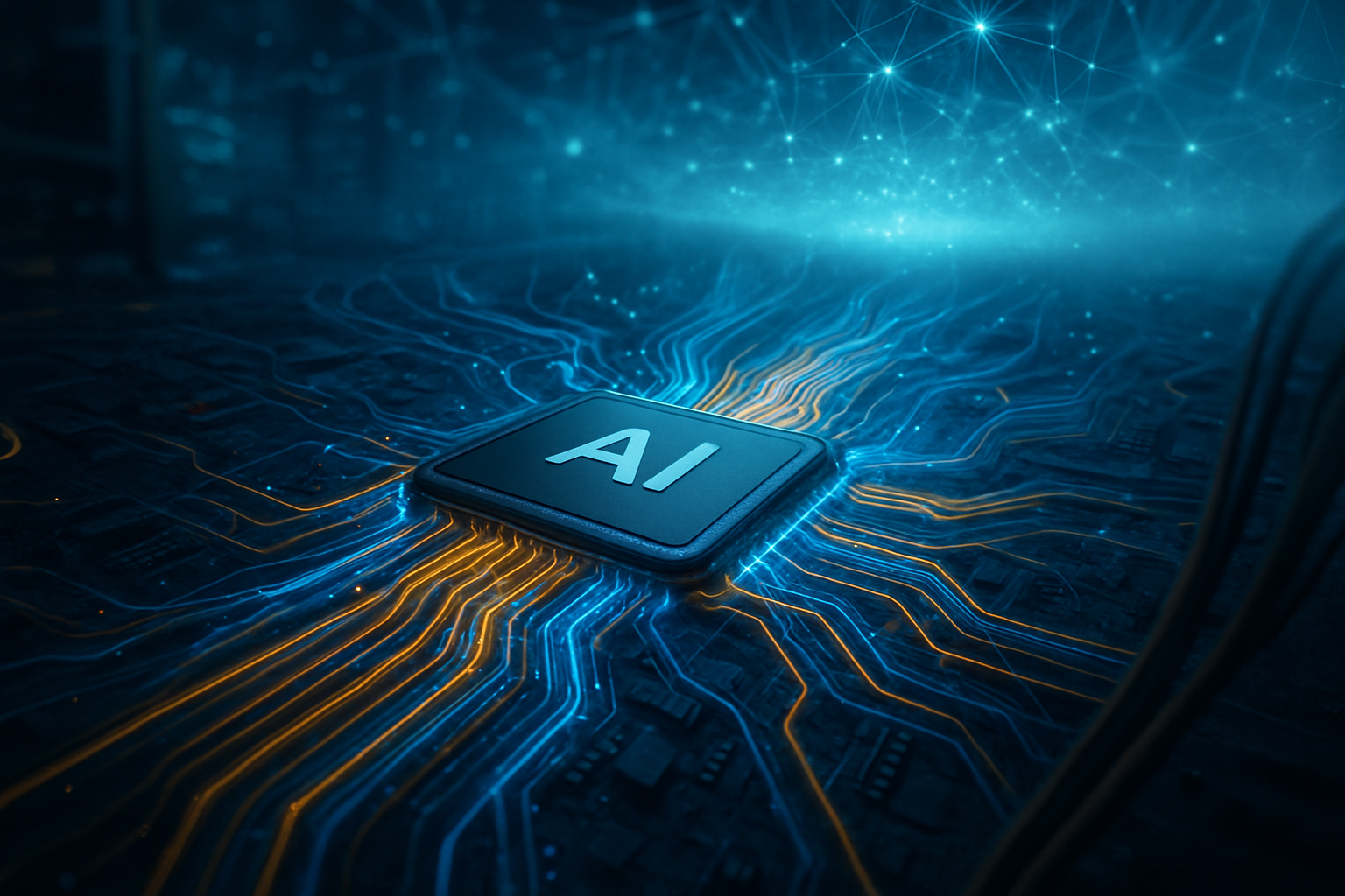
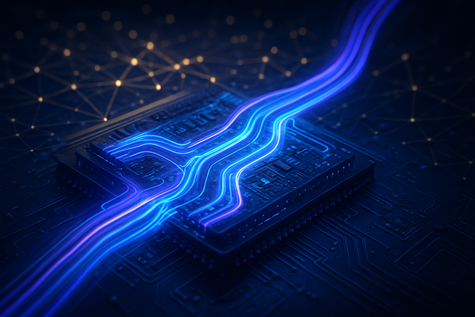
    The Technological Leap: Co-Packaged Optics and the 5 pJ/bit Milestone

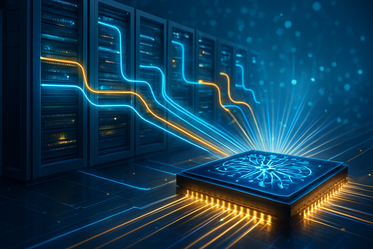
    The technical breakthrough at the center of this shift is the commercialization of Co-Packaged Optics (CPO). Unlike traditional pluggable transceivers that sit at the edge of a server rack, CPO integrates the optical engine directly onto the same package as the GPU or switch silicon. This proximity eliminates the need for power-hungry Digital Signal Processors (DSPs) to drive signals over long copper traces. In early 2026 deployments, this has reduced interconnect energy consumption from 15 picojoules per bit (pJ/bit) in 2024-era copper systems to less than 5 pJ/bit. Technical specifications for the latest optical I/O now boast up to 10x the bandwidth density of electrical pins, allowing for a "shoreline" of multi-terabit connectivity directly at the chip’s edge.

    Intel (NASDAQ: INTC) has achieved a major milestone by successfully integrating the laser and optical amplifiers directly onto the silicon photonics die (PIC) at scale. Their new Optical Compute Interconnect (OCI) chiplet, now being co-packaged with next-gen Xeon and Gaudi accelerators, supports 4 Tbps of bidirectional data transfer. Meanwhile, TSMC (NYSE: TSM) has entered mass production of its "Compact Universal Photonic Engine" (COUPE). This platform uses SoIC-X 3D stacking to bond an electrical die on top of a photonic die with copper-to-copper hybrid bonding, minimizing impedance to levels previously thought impossible. Initial reactions from the AI research community suggest that these advancements have effectively solved the "interconnect bottleneck," allowing for distributed training runs that perform as if they were running on a single, massive unified processor.

    Market Impact: NVIDIA, Broadcom, and the Strategic Re-Alignment

    The competitive landscape of the semiconductor industry is being redrawn by this optical revolution. NVIDIA (NASDAQ: NVDA) solidified its dominance during its January 2026 keynote by unveiling the "Rubin" platform. The successor to the Blackwell architecture, Rubin integrates HBM4 memory and is designed to interface directly with the Spectrum-X800 and Quantum-X800 photonic switches. These switches, developed in collaboration with TSMC, reduce laser counts by 4x compared to legacy modules while offering 5x better power efficiency per 1.6 Tbps port. This vertical integration allows NVIDIA to maintain its lead by offering a complete, light-speed ecosystem from the chip to the rack.

    Broadcom (NASDAQ: AVGO) has also asserted its leadership in high-radix optical switching with the volume shipping of "Davisson," the world’s first 102.4 Tbps Ethernet switch. By employing 16 integrated 6.4 Tbps optical engines, Broadcom has achieved a 70% power reduction over 2024-era pluggable modules. Furthermore, the strategic landscape shifted earlier this month with the confirmed acquisition of Celestial AI by Marvell (NASDAQ: MRVL) for $3.25 billion. Celestial AI’s "Photonic Fabric" technology allows GPUs to access up to 32TB of shared memory with less than 250ns of latency, treating remote memory as if it were local. This move positions Marvell as a primary challenger to NVIDIA in the race to build disaggregated, memory-centric AI data centers.

    Broader Significance: Sustainability and the End of the Memory Wall

    The wider significance of silicon photonics extends beyond mere speed; it is a matter of environmental and economic survival for the AI industry. As data centers began to consume an alarming percentage of the global power grid in 2025, the "power wall" threatened to halt AI progress. Optical interconnects provide a path toward sustainability by slashing the energy required for data movement, which previously accounted for a massive portion of a data center's thermal overhead. This shift allows hyperscalers like Microsoft (NASDAQ: MSFT) and Google (NASDAQ: GOOGL) to continue scaling their infrastructure without requiring the construction of a dedicated power plant for every new cluster.

    Moreover, the transition to light enables a new era of "disaggregated" computing. Historically, the distance between a CPU, GPU, and memory was limited by how far an electrical signal could travel before dying—usually just a few inches. With silicon photonics, high-speed signals can travel up to 2 kilometers with negligible loss. This allows for data center designs where entire racks of memory can be shared across thousands of GPUs, breaking the "memory wall" that has plagued LLM training. This milestone is comparable to the shift from vacuum tubes to silicon, as it fundamentally changes the physical geometry of how we build intelligent machines.

    Future Horizons: Toward Fully Optical Neural Networks

    Looking ahead, the industry is already eyeing the next frontier: fully optical neural networks and optical RAM. While current systems use light for communication and electricity for computation, researchers are working on "photonic computing" where the math itself is performed using the interference of light waves. Near-term, we expect to see the adoption of the Universal Chiplet Interconnect Express (UCIe) standard for optical links, which will allow for "mix-and-match" photonic chiplets from different vendors, such as Ayar Labs’ TeraPHY Gen 3, to be used in a single package.

    Challenges remain, particularly regarding the high-volume manufacturing of laser sources and the long-term reliability of co-packaged components in high-heat environments. However, experts predict that by 2027, optical I/O will be the standard for all data center silicon, not just high-end AI chips. We are moving toward a "Photonic Backbone" for the internet, where the latency between a user’s query and an AI’s response is limited only by the speed of light itself, rather than the resistance of copper wires.

    Conclusion: The Era of Light Arrives

    The move toward silicon photonics and optical interconnects represents a "hard reset" for computer architecture. By breaking the Copper Wall, the industry has cleared the path for the million-GPU clusters that will likely define the late 2020s. The key takeaways are clear: energy efficiency has improved by 3x, bandwidth density has increased by 10x, and the physical limits of the data center have been expanded from meters to kilometers.

    As we watch the coming weeks, the focus will shift to the first real-world benchmarks of NVIDIA’s Rubin and Broadcom’s Davisson systems in production environments. This development is not just a technical upgrade; it is the foundation for the next stage of human-AI evolution. The "Era of Light" has arrived, and with it, the promise of AI models that are faster, more efficient, and more capable than anything previously imagined.


    This content is intended for informational purposes only and represents analysis of current AI developments.

    TokenRing AI delivers enterprise-grade solutions for multi-agent AI workflow orchestration, AI-powered development tools, and seamless remote collaboration platforms.
    For more information, visit https://www.tokenring.ai/.

  • Shattering the Silicon Ceiling: Tower Semiconductor and LightIC Unveil Photonics Breakthrough to Power the Next Decade of AI and Autonomy

    Shattering the Silicon Ceiling: Tower Semiconductor and LightIC Unveil Photonics Breakthrough to Power the Next Decade of AI and Autonomy

    In a landmark announcement that signals a paradigm shift for both artificial intelligence infrastructure and autonomous mobility, Tower Semiconductor (NASDAQ: TSEM) and LightIC Technologies have unveiled a strategic partnership to mass-produce the world’s first monolithic 4D FMCW LiDAR and high-bandwidth optical interconnect chips. Announced on January 5, 2026, just days ahead of the Consumer Electronics Show (CES), this collaboration leverages Tower’s advanced 300mm silicon photonics (SiPho) foundry platform to integrate entire "optical benches"—lasers, modulators, and detectors—directly onto a single silicon substrate.

    The immediate significance of this development cannot be overstated. By successfully transitioning silicon photonics from experimental lab settings to high-volume manufacturing, the partnership addresses the two most critical bottlenecks in modern technology: the "memory wall" that limits AI model scaling in data centers and the high cost and unreliability of traditional sensing for autonomous vehicles. This breakthrough promises to slash power consumption in AI factories while providing self-driving systems with the "velocity awareness" required for safe urban navigation, effectively bridging the gap between digital and physical AI.

    The Technical Leap: 4D FMCW and the End of the Copper Era

    At the heart of the Tower-LightIC partnership is the commercialization of Frequency-Modulated Continuous-Wave (FMCW) LiDAR, a technology that differs fundamentally from the Time-of-Flight (ToF) systems currently used by most automotive manufacturers. While ToF LiDAR pulses light to measure distance, the new LightIC "Lark" and "FR60" chips utilize a continuous wave of light to measure both distance and instantaneous velocity—the fourth dimension—simultaneously for every pixel. This coherent detection method ensures that the sensors are immune to interference from sunlight or other LiDAR systems, a persistent challenge for existing technologies.

    Technically, the integration is achieved using Tower Semiconductor's PH18 process, which allows for the monolithic integration of III-V lasers with silicon-based optical components. The resulting "Lark" automotive chip boasts a detection range of up to 500 meters with a velocity precision of 0.05 meters per second. This level of precision allows a vehicle's AI to instantly distinguish between a stationary object and a pedestrian stepping into a lane, significantly reducing the "perception latency" that currently plagues autonomous driving stacks.

    Furthermore, the same silicon photonics platform is being applied to solve the data bottleneck within AI data centers. As AI models grow in complexity, the traditional copper interconnects used to move data between GPUs and High Bandwidth Memory (HBM) have become a liability, consuming excessive power and generating heat. The new optical interconnect chips enable multi-wavelength laser sources that provide bandwidth of up to 3.2 Tbps. By moving data via light rather than electricity, these chips reduce interconnect latency to a staggering 5 nanoseconds per meter, compared to the 15-20 picajoules per bit required by standard pluggable optics.

    Initial reactions from the AI research community have been overwhelmingly positive. Dr. Elena Vance, a senior researcher in photonics, noted that "the ability to manufacture these components on standard 300mm wafers at Tower's scale is the 'holy grail' of the industry. We are finally moving away from discrete, bulky optical components toward a truly integrated, solid-state future."

    Market Disruption: A New Hierarchy in AI Infrastructure

    The strategic alliance between Tower Semiconductor and LightIC creates immediate competitive pressure for industry giants like Nvidia (NASDAQ: NVDA), Marvell Technology (NASDAQ: MRVL), and Broadcom (NASDAQ: AVGO). While these companies have dominated the AI hardware space, the shift toward Co-Packaged Optics (CPO) and integrated silicon photonics threatens to disrupt established supply chains. Companies that can integrate photonics directly into their chipsets will hold a significant advantage in power efficiency and compute density.

    For data center operators like Amazon (NASDAQ: AMZN), Google (NASDAQ: GOOGL), and Meta (NASDAQ: META), this breakthrough offers a path toward "Green AI." As energy consumption in AI factories becomes a regulatory and financial hurdle, the transition to optical interconnects allows these giants to scale their clusters without hitting a thermal ceiling. The lower power profile of the Tower-LightIC chips could potentially reduce the total cost of ownership (TCO) for massive AI clusters by as much as 30% over a five-year period.

    In the automotive sector, the availability of low-cost, high-performance 4D LiDAR could democratize Level 4 and Level 5 autonomy. Currently, high-end LiDAR systems can cost thousands of dollars per unit, limiting them to luxury vehicles or experimental fleets. LightIC’s FR60 chip, designed for compact robotics and mass-market vehicles, aims to bring this cost down to a point where it can be standard equipment in entry-level consumer cars. This puts pressure on traditional sensor companies and may force a consolidation in the LiDAR market as solid-state silicon photonics becomes the dominant architecture.

    The Broader Significance: Toward "Physical AI" and Sustainability

    The convergence of sensing and communication on a single silicon platform marks a major milestone in the evolution of "Physical AI"—the application of artificial intelligence to the physical world through robotics and autonomous systems. By providing robots and vehicles with human-like (or better-than-human) perception at a fraction of the current energy cost, this breakthrough accelerates the timeline for truly autonomous logistics and urban mobility.

    This development also fits into the broader trend of "Compute-as-a-Light-Source." For years, the industry has warned of the "End of Moore’s Law" due to the physical limitations of shrinking transistors. Silicon photonics bypasses many of these limits by using photons instead of electrons for data movement. This is not just an incremental improvement; it is a fundamental shift in how information is processed and transported.

    However, the transition is not without its challenges. The shift to silicon photonics requires a complete overhaul of packaging and testing infrastructures. There are also concerns regarding the geopolitical nature of semiconductor manufacturing. As Tower Semiconductor expands its 300mm capacity, the strategic importance of foundry locations and supply chain resilience becomes even more pronounced. Nevertheless, the environmental impact of this technology—reducing the massive carbon footprint of AI training—is a significant positive that aligns with global sustainability goals.

    The Horizon: 1.6T Interconnects and Consumer-Grade Robotics

    Looking ahead, experts predict that the Tower-LightIC partnership is just the first wave of a photonics revolution. In the near term, we expect to see the release of 1.6T and 3.2T second-generation interconnects that will become the backbone of "GPT-6" class model training. These will likely be integrated into the next generation of AI supercomputers, enabling nearly instantaneous data sharing across thousands of nodes.

    In the long term, the "FR60" compact LiDAR chip is expected to find its way into consumer electronics beyond the automotive sector. Potential applications include high-precision spatial computing for AR/VR headsets and sophisticated obstacle avoidance for consumer-grade drones and home service robots. The challenge will be maintaining high yields during the mass-production phase, but Tower’s proven track record in analog and mixed-signal manufacturing provides a strong foundation for success.

    Industry analysts predict that by 2028, silicon photonics will account for over 40% of the total data center interconnect market. "The era of the electron is giving way to the era of the photon," says market analyst Marcus Thorne. "What we are seeing today is the foundation for the next twenty years of computing."

    A New Chapter in Semiconductor History

    The partnership between Tower Semiconductor and LightIC Technologies represents a definitive moment in the history of semiconductors. By solving the data bottleneck in AI data centers and providing a high-performance, low-cost solution for autonomous sensing, these two companies have cleared the path for the next generation of AI-driven innovation.

    The key takeaway for the industry is that the integration of optical and electrical components is no longer a futuristic concept—it is a manufacturing reality. As these chips move into mass production throughout 2026, the tech world will be watching closely to see how quickly they are adopted by the major cloud providers and automotive OEMs. This development is not just about faster chips or better sensors; it is about enabling a future where AI can operate seamlessly and sustainably in both the digital and physical realms.

    In the coming months, keep a close eye on the initial deployment of "Lark" B-samples in automotive pilot programs and the first integration of Tower’s 3.2T optical engines in commercial AI clusters. The light-speed revolution has officially begun.


    This content is intended for informational purposes only and represents analysis of current AI developments.

    TokenRing AI delivers enterprise-grade solutions for multi-agent AI workflow orchestration, AI-powered development tools, and seamless remote collaboration platforms.
    For more information, visit https://www.tokenring.ai/.

  • Breaking the Copper Wall: Co-Packaged Optics and Silicon Photonics Usher in the Million-GPU Era

    Breaking the Copper Wall: Co-Packaged Optics and Silicon Photonics Usher in the Million-GPU Era

    As of January 8, 2026, the artificial intelligence industry has officially collided with a physical limit known as the "Copper Wall." At data transfer speeds of 224 Gbps and beyond, traditional copper wiring can no longer carry signals more than a few inches without massive signal degradation and unsustainable power consumption. To circumvent this, the world’s leading semiconductor and networking firms have pivoted to Co-Packaged Optics (CPO) and Silicon Photonics, a paradigm shift that integrates fiber-optic communication directly into the chip package. This breakthrough is not just an incremental upgrade; it is the foundational technology enabling the first million-GPU clusters and the training of trillion-parameter AI models.

    The immediate significance of this transition is staggering. By moving the conversion of electrical signals to light (photonics) from separate pluggable modules directly onto the processor or switch substrate, companies are slashing energy consumption by up to 70%. In an era where data center power demands are straining national grids, the ability to move data at 102.4 Tbps while significantly reducing the "tax" of data movement has become the most critical metric in the AI arms race.

    The technical specifications of the current 2026 hardware generation highlight a massive leap over the pluggable optics of 2024. Broadcom Inc. (NASDAQ: AVGO) has begun volume shipping its "Davisson" Tomahawk 6 switch, the industry’s first 102.4 Tbps Ethernet switch. This device utilizes 16 integrated 6.4 Tbps optical engines, leveraging TSMC’s Compact Universal Photonic Engine (COUPE) technology. Unlike previous generations that relied on power-hungry Digital Signal Processors (DSPs) to push signals through copper traces, CPO systems like Davisson use "Direct Drive" architectures. This eliminates the DSP entirely for short-reach links, bringing energy efficiency down from 15–20 picojoules per bit (pJ/bit) to a mere 5 pJ/bit.

    NVIDIA (NASDAQ: NVDA) has similarly embraced this shift with its Quantum-X800 InfiniBand platform. By utilizing micro-ring modulators, NVIDIA has achieved a bandwidth density of over 1.0 Tbps per millimeter of chip "shoreline"—a five-fold increase over traditional methods. This density is crucial because the physical perimeter of a chip is limited; silicon photonics allows dozens of data channels to be multiplexed onto a single fiber using Wavelength Division Multiplexing (WDM), effectively bypassing the physical constraints of electrical pins.

    The research community has hailed these developments as the "end of the pluggable era." Early reactions from the Open Compute Project (OCP) suggest that the shift to CPO has solved the "Distance-Speed Tradeoff." Previously, high-speed signals were restricted to distances of less than one meter. With silicon photonics, these same signals can now travel up to 2 kilometers with negligible latency (5–10ns compared to the 100ns+ required by DSP-based systems), allowing for "disaggregated" data centers where compute and memory can be located in different racks while behaving as a single monolithic machine.

    The commercial landscape for AI infrastructure is being radically reshaped by this optical transition. Broadcom and NVIDIA have emerged as the primary beneficiaries, having successfully integrated photonics into their core roadmaps. NVIDIA’s latest "Rubin" R100 platform, which entered production in late 2025, makes CPO mandatory for its rack-scale architecture. This move forces competitors to either develop similar in-house photonic capabilities or rely on third-party chiplet providers like Ayar Labs, which recently reached high-volume production of its TeraPHY optical I/O chiplets.

    Intel Corporation (NASDAQ: INTC) has also pivoted its strategy, having divested its traditional pluggable module business to Jabil in late 2024 to focus exclusively on high-value Optical Compute Interconnect (OCI) chiplets. Intel’s OCI is now being sampled by major cloud providers, offering a standardized way to add optical I/O to custom AI accelerators. Meanwhile, Marvell Technology (NASDAQ: MRVL) is positioning itself as the leader in the "Scale-Up" market, using its acquisition of Celestial AI’s photonic fabric to power the next generation of UALink-compatible switches, which are expected to sample in the second half of 2026.

    This shift creates a significant barrier to entry for smaller AI chip startups. The complexity of 2.5D and 3D packaging required to co-package optics with silicon is immense, requiring deep partnerships with foundries like TSMC and specialized OSAT (Outsourced Semiconductor Assembly and Test) providers. Major AI labs, such as OpenAI and Anthropic, are now factoring "optical readiness" into their long-term compute contracts, favoring providers who can offer the lower TCO (Total Cost of Ownership) and higher reliability that CPO provides.

    The wider significance of Co-Packaged Optics lies in its impact on the "Power Wall." A cluster of 100,000 GPUs using traditional interconnects can consume over 60 Megawatts just for data movement. By switching to CPO, data center operators can reclaim that power for actual computation, effectively increasing the "AI work per watt" by a factor of three. This is a critical development for global sustainability goals, as the energy footprint of AI has become a point of intense regulatory scrutiny in early 2026.

    Furthermore, CPO addresses the long-standing issue of reliability in large-scale systems. In the past, the laser—the most failure-prone component of an optical link—was embedded deep inside the chip package, making a single laser failure a catastrophic event for a $40,000 GPU. The 2026 generation of hardware has standardized the External Laser Source (ELSFP), a field-replaceable unit that keeps the heat-generating laser away from the compute silicon. This "pluggable laser" approach combines the reliability of traditional optics with the performance of co-packaging.

    Comparisons are already being drawn to the introduction of High Bandwidth Memory (HBM) in 2015. Just as HBM solved the "Memory Wall" by moving memory closer to the processor, CPO is solving the "Interconnect Wall" by moving the network into the package. This evolution suggests that the future of AI scaling is no longer about making individual chips faster, but about making the entire data center act as a single, fluid fabric of light.

    Looking ahead, the next 24 months will likely see the integration of silicon photonics directly with HBM4. This would allow for "Optical CXL," where a GPU could access memory located hundreds of meters away with the same latency as local on-board memory. Experts predict that by 2027, we will see the first all-optical backplanes, eliminating copper from the data center fabric entirely.

    However, challenges remain. The industry is still debating the standardization of optical interfaces. While the Ultra Accelerator Link (UALink) consortium has made strides, a "standards war" between InfiniBand-centric and Ethernet-centric optical implementations continues. Additionally, the yield rates for 3D-stacked silicon photonics remain lower than traditional CMOS, though they are improving as TSMC and Intel refine their specialized photonic processes.

    The most anticipated development for late 2026 is the deployment of 1.6T and 3.2T optical links per lane. As AI models move toward "World Models" and multi-modal reasoning that requires massive real-time data ingestion, these speeds will transition from a luxury to a necessity. Experts predict that the first "Exascale AI" system, capable of a quintillion operations per second, will be built entirely on a silicon photonics foundation.

    The transition to Co-Packaged Optics and Silicon Photonics represents a watershed moment in the history of computing. By breaking the "Copper Wall," the industry has ensured that the scaling laws of AI can continue for at least another decade. The move from 20 pJ/bit to 5 pJ/bit is not just a technical win; it is an economic and environmental necessity that enables the massive infrastructure projects currently being planned by the world's largest technology companies.

    As we move through 2026, the key metrics to watch will be the volume ramp-up of Broadcom’s Tomahawk 6 and the field performance of NVIDIA’s Rubin platform. If these systems deliver on their promise of 70% power reduction and 10x bandwidth density, the "Optical Era" will be firmly established as the backbone of the AI revolution. The light-speed data center is no longer a laboratory dream; it is the reality of the 2026 AI landscape.


    This content is intended for informational purposes only and represents analysis of current AI developments.

    TokenRing AI delivers enterprise-grade solutions for multi-agent AI workflow orchestration, AI-powered development tools, and seamless remote collaboration platforms.
    For more information, visit https://www.tokenring.ai/.

  • The Silicon Photonics Revolution: Tower Semiconductor and LightIC Unveil 4D FMCW LiDAR for the Age of Physical AI

    The Silicon Photonics Revolution: Tower Semiconductor and LightIC Unveil 4D FMCW LiDAR for the Age of Physical AI

    On January 5, 2026, the landscape of autonomous sensing underwent a seismic shift as Tower Semiconductor (NASDAQ: TSEM) and LightIC Technologies announced a landmark strategic collaboration. The partnership is designed to mass-produce the next generation of Silicon Photonics (SiPho)-based 4D FMCW LiDAR, marking a pivotal moment where high-speed optical technology—once confined to the massive data centers powering Large Language Models—finally transitions into the "Physical AI" domain. This move promises to bring high-performance, velocity-aware sensing to autonomous vehicles and robotics at a scale and price point previously thought impossible.

    The collaboration leverages Tower Semiconductor’s mature 300mm SiPho foundry platform to manufacture LightIC’s proprietary Frequency-Modulated Continuous-Wave (FMCW) chips. By integrating complex optical engines—including lasers, modulators, and detectors—onto a single silicon substrate, the two companies are addressing the "SWaP-C" (Size, Weight, Power, and Cost) barriers that have long hindered the widespread adoption of high-end LiDAR. As AI models move from generating text to controlling physical "atoms" in robots and cars, this development provides the high-fidelity sensory input required for machines to navigate complex, dynamic human environments with unprecedented safety.

    The Technical Edge: 4D FMCW and the End of Optical Interference

    At the heart of this announcement are two flagship products: the Lark™ for long-range automotive use and the FR60™ for compact robotics. Unlike traditional Time-of-Flight (ToF) LiDAR systems used by many current autonomous platforms, which measure distance by timing the reflection of light pulses, LightIC’s 4D FMCW technology measures both distance and instantaneous velocity simultaneously. The Lark™ system boasts a detection range of up to 300 meters and can identify objects at 500 meters, while providing velocity data with a precision of 0.05 m/s. This "4D" capability allows the AI to immediately distinguish between a stationary object and one moving toward the vehicle, drastically reducing the computational latency required for multi-frame tracking.

    Technically, the transition to SiPho allows these systems to operate at the 1550nm wavelength, which is inherently safer for human eyes and allows for higher power output than the 905nm lasers used in cheaper ToF systems. Furthermore, FMCW is naturally immune to optical interference. In a future where hundreds of autonomous vehicles might occupy the same highway, traditional LiDARs can "blind" each other with overlapping pulses. LightIC’s coherent detection ensures that each sensor only "hears" its own unique frequency-modulated signal, effectively eliminating the "crosstalk" problem that has plagued the industry.

    The manufacturing process is equally significant. Tower Semiconductor utilizes its PH18 SiPho process and advanced wafer bonding to create a monolithic "LiDAR-on-a-chip." This differs from previous approaches that relied on discrete components—individual lasers and lenses—which are difficult to align and prone to failure under the vibrations of automotive use. By moving the entire optical bench onto a silicon chip, the partnership enables "image-grade" point clouds with an angular resolution of 0.1° x 0.08°, providing the resolution of a high-definition camera with the depth precision of a laser.

    Reshaping the Competitive Landscape: The Foundry Advantage

    This development is a direct challenge to established LiDAR players and represents a strategic win for the foundry model in photonics. While companies like Hesai Group (NASDAQ: HSAI) and Luminar Technologies (NASDAQ: LAZR) have made strides in automotive integration, the Tower-LightIC partnership brings the economies of scale associated with semiconductor giants. By utilizing the same 300mm manufacturing lines that produce 1.6Tbps optical transceivers for companies like NVIDIA Corporation (NASDAQ: NVDA), the partnership can drive down the cost of high-end LiDAR to levels that make it viable for mass-market consumer vehicles, not just luxury fleets or robotaxis.

    For AI labs and robotics startups, this announcement is a major enabler. The "Physical AI" movement—led by entities like Tesla, Figure, and Boston Dynamics—relies on high-quality training data. The ability to feed a neural network real-time, per-point velocity data rather than just 3D coordinates simplifies the "perception-to-action" pipeline. This could disrupt the current market for secondary sensors, potentially reducing the reliance on complex radar-camera fusion by providing a single, high-fidelity source of truth.

    Beyond Vision: The Arrival of "Velocity-Aware" Physical AI

    The broader significance of this expansion lies in the evolution of the AI landscape itself. For the past several years, the "AI Revolution" has been largely digital, focused on processing information within the cloud. In 2026, the trend has shifted toward "Embodied AI" or "Physical AI," where the challenge is to give silicon brains the ability to interact safely with the physical world. Silicon Photonics is the bridge for this transition. Just as CMOS image sensors revolutionized the smartphone era by making high-quality cameras ubiquitous, SiPho is poised to do the same for 3D sensing.

    The move from data centers to the edge is a natural progression. The photonics industry spent a decade perfecting the reliability and throughput of optical interconnects to handle the massive traffic of AI training clusters. That same reliability is now being applied to automotive safety. The implications for safety are profound: a vehicle equipped with 4D FMCW LiDAR can "see" the intention of a pedestrian or another vehicle through their instantaneous velocity, allowing for much faster emergency braking or evasive maneuvers. This level of "velocity awareness" is a milestone in the quest for Level 4 and Level 5 autonomy.

    The Road Ahead: Scaling Autonomy from Highways to Households

    In the near term, expect to see the Lark™ system integrated into high-end electric vehicle platforms scheduled for late 2026 and 2027 releases. The compact FR60™ is likely to find an immediate home in the logistics sector, powering the next generation of autonomous mobile robots (AMRs) in warehouses and "last-mile" delivery bots. The challenge moving forward will not be the hardware itself, but the software integration. AI developers will need to rewrite perception stacks to take full advantage of the 4D data stream, moving away from legacy algorithms designed for 3D ToF sensors.

    Experts predict that the success of the Tower-LightIC collaboration will spark a wave of consolidation in the LiDAR industry. Smaller players without access to high-volume SiPho foundries may struggle to compete on price and performance. As we look toward 2027, the goal will be "ubiquitous sensing"—integrating these chips into everything from household service robots to smart infrastructure. The "invisible AI" layer is becoming a reality, where the machines around us possess a sense of sight and motion that exceeds human capability.

    Conclusion: A New Foundation for Intelligent Machines

    The collaboration between Tower Semiconductor and LightIC Technologies marks the official entry of Silicon Photonics into the mainstream of Physical AI. By solving the dual challenges of interference and cost through advanced semiconductor manufacturing, they have provided the "eyes" that the next generation of AI requires. This is more than just a hardware upgrade; it is a foundational shift in how machines perceive reality.

    As we move through 2026, the industry will be watching for the first road tests of these integrated chips and the subsequent performance benchmarks from the robotics community. The transition of SiPho from the silent racks of data centers to the bustling streets of our cities is a testament to the technology's maturity. For the AI industry, the message is clear: the brain has been built, and now, it finally has the vision to match.


    This content is intended for informational purposes only and represents analysis of current AI developments.

    TokenRing AI delivers enterprise-grade solutions for multi-agent AI workflow orchestration, AI-powered development tools, and seamless remote collaboration platforms.
    For more information, visit https://www.tokenring.ai/.

  • The Speed of Light: Marvell’s Acquisition of Celestial AI Signals the End of the Copper Era in AI Computing

    The Speed of Light: Marvell’s Acquisition of Celestial AI Signals the End of the Copper Era in AI Computing

    In a move that marks a fundamental shift in the architecture of artificial intelligence, Marvell Technology (NASDAQ: MRVL) announced on December 2, 2025, a definitive agreement to acquire the silicon photonics trailblazer Celestial AI for a total potential value of over $5.5 billion. This acquisition, expected to close in the first quarter of 2026, represents the most significant bet yet on the transition from copper-based electrical signals to light-based optical interconnects within the heart of the data center. By integrating Celestial AI’s "Photonic Fabric" technology, Marvell is positioning itself to dismantle the "Memory Wall" and "Power Wall" that have threatened to stall the progress of large-scale AI models.

    The immediate significance of this deal cannot be overstated. As AI clusters scale toward a million GPUs, the physical limitations of copper—the "Copper Cliff"—have become the primary bottleneck for performance and energy efficiency. Conventional copper wires generate excessive heat and suffer from signal degradation over short distances, forcing engineers to use power-hungry chips to boost signals. Marvell’s absorption of Celestial AI’s technology effectively replaces these electrons with photons, allowing for nearly instantaneous data transfer between processors and memory at a fraction of the power, fundamentally changing how AI hardware is designed and deployed.

    Breaking the Copper Wall: The Photonic Fabric Breakthrough

    At the technical core of this development is Celestial AI’s proprietary Photonic Fabric™, an architecture that moves optical I/O (Input/Output) from the edge of the circuit board directly into the silicon package. Traditionally, optical components were "pluggable" modules located at the periphery, requiring long electrical traces to reach the processor. Celestial AI’s Optical Multi-Chip Interconnect Bridge (OMIB) utilizes 3D optical co-packaging, allowing light-based data paths to sit directly atop the compute die. This "in-package" optics approach frees up the valuable "beachfront property" on the edges of the chip, which can now be dedicated entirely to High Bandwidth Memory (HBM).

    This shift differs from previous approaches by eliminating the need for power-hungry Digital Signal Processors (DSPs) traditionally required for optical-to-electrical conversion. The Photonic Fabric utilizes a "linear-drive" method, achieving nanosecond-class latency and reducing interconnect power consumption by over 80%. While copper interconnects typically consume 50–55 picojoules per bit (pJ/bit) at scale, Marvell’s new photonic architecture operates at approximately 2.4 pJ/bit. This efficiency is critical as the industry moves toward 2nm process nodes, where every milliwatt of power saved in data transfer can be redirected toward actual computation.

    Initial reactions from the AI research community and industry experts have been overwhelmingly positive, with many describing the move as the "missing link" for the next generation of AI supercomputing. Dr. Arati Prabhakar, an industry analyst specializing in semiconductor physics, noted that "moving optics into the package is no longer a luxury; it is a physical necessity for the post-GPT-5 era." By supporting emerging standards like UALink (Ultra Accelerator Link) and CXL 3.1, Marvell is providing an open-standard alternative to proprietary interconnects, a move that has been met with enthusiasm by researchers looking for more flexible cluster architectures.

    A New Battleground: Marvell vs. the Proprietary Giants

    The acquisition places Marvell Technology (NASDAQ: MRVL) in a direct competitive collision with NVIDIA (NASDAQ: NVDA), whose proprietary NVLink technology has long been the gold standard for high-speed GPU interconnectivity. By offering an optical fabric that is compatible with industry-standard protocols, Marvell is giving hyperscalers like Amazon (NASDAQ: AMZN) and Alphabet (NASDAQ: GOOGL) a way to build massive AI clusters without being "locked in" to a single vendor’s ecosystem. This strategic positioning allows Marvell to act as the primary architect for the connectivity layer of the AI stack, potentially disrupting the dominance of integrated hardware providers.

    Other major players in the networking space, such as Broadcom (NASDAQ: AVGO), are also feeling the heat. While Broadcom has led in traditional Ethernet switching, Marvell’s integration of Celestial AI’s 3D-stacked optics gives them a head start in "Scale-Up" networking—the ultra-fast connections between individual GPUs and memory pools. This capability is essential for "disaggregated" computing, where memory and compute are no longer tethered to the same physical board but can be pooled across a rack via light, allowing for much more efficient resource utilization in the data center.

    For AI startups and smaller chip designers, this breakthrough lowers the barrier to entry for high-performance computing. By utilizing Marvell’s custom ASIC (Application-Specific Integrated Circuit) platforms integrated with Photonic Fabric chiplets, smaller firms can design specialized AI accelerators that rival the performance of industry giants. This democratization of high-speed interconnects could lead to a surge in specialized "Super XPUs" tailored for specific tasks like real-time video synthesis or complex biological modeling, further diversifying the AI hardware landscape.

    The Wider Significance: Sustainability and the Scaling Limit

    Beyond the competitive maneuvering, the shift to silicon photonics addresses the growing societal concern over the environmental impact of AI. Data centers are currently on a trajectory to consume a massive percentage of the world’s electricity, with a significant portion of that energy wasted as heat generated by electrical resistance in copper wires. By slashing interconnect power by 80%, the Marvell-Celestial AI breakthrough offers a rare "green" win in the AI arms race. This reduction in heat also simplifies cooling requirements, potentially allowing for denser, more powerful data centers in urban areas where power and space are at a premium.

    This milestone is being compared to the transition from vacuum tubes to transistors in the mid-20th century. Just as the transistor allowed for a leap in miniaturization and efficiency, the move to silicon photonics allows for a leap in "cluster-scale" computing. We are moving away from the "box-centric" model, where a single server is the unit of compute, toward a "fabric-centric" model where the entire data center functions as one giant, light-speed brain. This shift is essential for training the next generation of foundation models, which are expected to require hundreds of trillions of parameters—a scale that copper simply cannot support.

    However, the transition is not without its concerns. The complexity of manufacturing 3D-stacked optical components is significantly higher than traditional silicon, raising questions about yield rates and supply chain stability. There is also the challenge of laser reliability; unlike transistors, lasers can degrade over time, and integrating them directly into the processor package makes them difficult to replace. The industry will need to develop new testing and maintenance protocols to ensure that these light-driven supercomputers can operate reliably for years at a time.

    Looking Ahead: The Era of the Super XPU

    In the near term, the industry can expect to see the first "Super XPUs" featuring integrated optical I/O hitting the market by early 2027. These chips will likely debut in the custom silicon projects of major hyperscalers before becoming more widely available. The long-term development will likely focus on "Co-Packaged Optics" (CPO) becoming the standard for all high-performance silicon, eventually trickling down from AI data centers to high-end workstations and perhaps even consumer-grade edge devices as the technology matures and costs decrease.

    The next major challenge for Marvell and its competitors will be the integration of these optical fabrics with "optical computing" itself—using light not just to move data, but to perform calculations. While still in the experimental phase, the marriage of optical interconnects and optical processing could lead to a thousand-fold increase in AI efficiency. Experts predict that the next five years will be defined by this "Photonic Revolution," as the industry works to replace every remaining electrical bottleneck with a light-based alternative.

    Conclusion: A Luminous Path Forward

    The acquisition of Celestial AI by Marvell Technology (NASDAQ: MRVL) is more than just a corporate merger; it is a declaration that the era of copper in high-performance computing is drawing to a close. By successfully integrating photons into the silicon package, Marvell has provided the roadmap for scaling AI beyond the physical limits of electricity. The key takeaways are clear: latency is being measured in nanoseconds, power consumption is being slashed by orders of magnitude, and the very architecture of the data center is being rewritten in light.

    This development will be remembered as a pivotal moment in AI history, the point where hardware finally caught up with the soaring ambitions of software. As we move into 2026 and beyond, the industry will be watching closely to see how quickly Marvell can scale this technology and how its competitors respond. For now, the path to artificial general intelligence looks increasingly luminous, powered by a fabric of light that promises to connect the world's most powerful minds—both human and synthetic—at the speed of thought.


    This content is intended for informational purposes only and represents analysis of current AI developments.

    TokenRing AI delivers enterprise-grade solutions for multi-agent AI workflow orchestration, AI-powered development tools, and seamless remote collaboration platforms.
    For more information, visit https://www.tokenring.ai/.

  • Shattering the Copper Wall: Silicon Photonics Ushers in the Age of Light-Speed AI Clusters

    Shattering the Copper Wall: Silicon Photonics Ushers in the Age of Light-Speed AI Clusters

    As of January 6, 2026, the global technology landscape has reached a definitive crossroads in the evolution of artificial intelligence infrastructure. For decades, the movement of data within the heart of the world’s most powerful computers relied on the flow of electrons through copper wires. However, the sheer scale of modern AI—typified by the emergence of "million-GPU" clusters and the push toward Artificial General Intelligence (AGI)—has officially pushed copper to its physical breaking point. The industry has entered the "Silicon Photonics Era," a transition where light replaces electricity as the primary medium for data center interconnects.

    This shift is not merely a technical upgrade; it is a fundamental re-architecting of how AI models are built and scaled. With the "Copper Wall" rendering traditional electrical signaling inefficient at speeds beyond 224 Gbps, the world’s leading semiconductor and cloud giants have pivoted to optical fabrics. By integrating lasers and photonic circuits directly into the silicon package, the industry has unlocked a 70% reduction in interconnect power consumption while doubling bandwidth, effectively clearing the path for the next decade of AI growth.

    The Physics of the 'Copper Wall' and the Rise of 1.6T Optics

    The technical crisis that precipitated this shift is known as the "Copper Wall." As per-lane speeds reached 224 Gbps in late 2024 and throughout 2025, the reach of passive copper cables plummeted to less than one meter. At these frequencies, electrical signals degrade so rapidly that they can barely traverse a single server rack without massive power-hungry amplification. By early 2025, data center operators reported that the "I/O Tax"—the energy required just to move data between chips—was consuming nearly 30% of total cluster power.

    To solve this, the industry has turned to Co-Packaged Optics (CPO) and Silicon Photonics. Unlike traditional pluggable transceivers that sit at the edge of a switch, CPO moves the optical engine directly onto the processor substrate. This allows for a "shoreline" of high-speed optical I/O that bypasses the energy losses of long electrical traces. In late 2025, the market saw the mass adoption of 1.6T (Terabit) transceivers, which utilize 200G per-lane technology. By early 2026, initial demonstrations of 3.2T links using 400G per-lane technology have already begun, promising to support the massive throughput required for real-time inference on trillion-parameter models.

    The technical community has also embraced Linear-drive Pluggable Optics (LPO) as a bridge technology. By removing the power-intensive Digital Signal Processor (DSP) from the optical module and relying on the host ASIC to drive the signal, LPO has provided a lower-latency, lower-power intermediate step. However, for the most advanced AI clusters, CPO is now considered the "gold standard," as it reduces energy consumption from approximately 15 picojoules per bit (pJ/bit) to less than 5 pJ/bit.

    The New Power Players: NVDA, AVGO, and the Optical Arms Race

    The transition to light has fundamentally shifted the competitive dynamics among semiconductor giants. Nvidia (NASDAQ: NVDA) has solidified its dominance by integrating silicon photonics into its latest Rubin architecture and Quantum-X networking platforms. By utilizing optical NVLink fabrics, Nvidia’s million-GPU clusters can now operate with nanosecond latency, effectively treating an entire data center as a single, massive GPU.

    Broadcom (NASDAQ: AVGO) has emerged as a primary architect of this new era with its Tomahawk 6-Davisson switch, which boasts a staggering 102.4 Tbps throughput and integrated CPO. Broadcom’s success in proving CPO reliability at scale—particularly within the massive AI infrastructures of Meta and Google—has made it the indispensable partner for optical networking. Meanwhile, TSMC (NYSE: TSM) has become the foundational foundry for this transition through its COUPE (Compact Universal Photonic Engine) technology, which allows for the 3D stacking of photonic and electronic circuits, a feat previously thought to be years away from mass production.

    Other key players are carving out critical niches in the optical ecosystem. Marvell (NASDAQ: MRVL), following its strategic acquisition of optical interconnect startups in late 2025, has positioned its Ara 1.6T Optical DSP as the backbone for third-party AI accelerators. Intel (NASDAQ: INTC) has also made a significant comeback in the data center space with its Optical Compute Interconnect (OCI) chiplets. Intel’s unique ability to integrate lasers directly onto the silicon die has enabled "disaggregated" data centers, where compute and memory can be physically separated by over 100 meters without a loss in performance, a capability that is revolutionizing how hyperscalers design their facilities.

    Sustainability and the Global Interconnect Pivot

    The wider significance of the move from copper to light extends far beyond mere speed. In an era where the energy demands of AI have become a matter of national security and environmental concern, silicon photonics offers a rare "win-win" for both performance and sustainability. The 70% reduction in interconnect power provided by CPO is critical for meeting the carbon-neutral goals of tech giants like Microsoft and Amazon, who are currently retrofitting their global data center fleets to support optical fabrics.

    Furthermore, this transition marks the end of the "Compute-Bound" era and the beginning of the "Interconnect-Bound" era. For years, the bottleneck in AI was the speed of the processor itself. Today, the bottleneck is the "fabric"—the ability to move massive amounts of data between thousands of processors simultaneously. By shattering the Copper Wall, the industry has ensured that AI scaling laws can continue to hold true for the foreseeable future.

    However, this shift is not without its concerns. The complexity of manufacturing CPO-based systems is significantly higher than traditional copper-based ones, leading to potential supply chain vulnerabilities. There are also ongoing debates regarding the "serviceability" of integrated optics; if an optical laser fails inside a $40,000 GPU package, the entire unit may need to be replaced, unlike the "hot-swappable" pluggable modules of the past.

    The Road to Petabit Connectivity and Optical Computing

    Looking ahead to the remainder of 2026 and into 2027, the industry is already eyeing the next frontier: Petabit-per-second connectivity. As 3.2T transceivers move into production, researchers are exploring multi-wavelength "comb lasers" that can transmit hundreds of data streams over a single fiber, potentially increasing bandwidth density by another order of magnitude.

    Beyond just moving data, the ultimate goal is Optical Computing—performing mathematical calculations using light itself rather than transistors. While still in the early experimental stages, the integration of photonics into the processor package is the necessary first step toward this "Holy Grail" of computing. Experts predict that by 2028, we may see the first hybrid "Opto-Electronic" processors that perform specific AI matrix multiplications at the speed of light, with virtually zero heat generation.

    The immediate challenge remains the standardization of CPO interfaces. Groups like the OIF (Optical Internetworking Forum) are working feverishly to ensure that components from different vendors can interoperate, preventing the "walled gardens" that could stifle innovation in the optical ecosystem.

    Conclusion: A Bright Future for AI Infrastructure

    The transition from copper to silicon photonics represents one of the most significant architectural shifts in the history of computing. By overcoming the physical limitations of electricity, the industry has laid the groundwork for AGI-scale infrastructure that is faster, more efficient, and more scalable than anything that came before. The "Copper Era," which defined the first fifty years of the digital age, has finally given way to the "Era of Light."

    As we move further into 2026, the key metrics to watch will be the yield rates of CPO-integrated chips and the speed at which 1.6T networking is deployed across global data centers. For AI companies and tech enthusiasts alike, the message is clear: the future of intelligence is no longer traveling through wires—it is moving at the speed of light.


    This content is intended for informational purposes only and represents analysis of current AI developments.

    TokenRing AI delivers enterprise-grade solutions for multi-agent AI workflow orchestration, AI-powered development tools, and seamless remote collaboration platforms.
    For more information, visit https://www.tokenring.ai/.

  • The Speed of Light: Silicon Photonics and the End of the Copper Era in AI Data Centers

    The Speed of Light: Silicon Photonics and the End of the Copper Era in AI Data Centers

    As the calendar turns to 2026, the artificial intelligence industry has arrived at a pivotal architectural crossroads. For decades, the movement of data within computers has relied on the flow of electrons through copper wiring. However, as AI clusters scale toward the "million-GPU" milestone, the physical limits of electricity—long whispered about as the "Copper Wall"—have finally been reached. In the high-stakes race to build the infrastructure for Artificial General Intelligence (AGI), the industry is officially abandoning traditional electrical interconnects in favor of Silicon Photonics and Co-Packaged Optics (CPO).

    This transition marks one of the most significant shifts in computing history. By integrating laser-based data transmission directly onto the silicon chip, industry titans like Broadcom (NASDAQ:AVGO) and NVIDIA (NASDAQ:NVDA) are enabling petabit-per-second connectivity with energy efficiency that was previously thought impossible. The arrival of these optical "superhighways" in early 2026 signals the end of the copper era in high-performance data centers, effectively decoupling bandwidth growth from the crippling power constraints that threatened to stall AI progress.

    Breaking the Copper Wall: The Technical Leap to CPO

    The technical crisis necessitating this shift is rooted in the physics of 224 Gbps signaling. At these speeds, the reach of traditional passive copper cables has shrunk to less than one meter, and the power required to force electrical signals through these wires has skyrocketed. In early 2025, data center operators reported that interconnects were consuming nearly 30% of total cluster power. The solution, arriving in volume this year, is Co-Packaged Optics. Unlike traditional pluggable transceivers that sit on the edge of a switch, CPO brings the optical engine directly into the chip's package.

    Broadcom (NASDAQ:AVGO) has set the pace with its 2026 flagship, the Tomahawk 6-Davisson switch. Boasting a staggering 102.4 Terabits per second (Tbps) of aggregate capacity, the Davisson utilizes TSMC (NYSE:TSM) COUPE technology to stack photonic engines directly onto the switching silicon. This integration reduces data transmission energy by over 70%, moving from roughly 15 picojoules per bit (pJ/bit) in traditional systems to less than 5 pJ/bit. Meanwhile, NVIDIA (NASDAQ:NVDA) has launched its Quantum-X Photonics InfiniBand platform, specifically designed to link its "million-GPU" clusters. These systems replace bulky copper cables with thin, liquid-cooled fiber optics that provide 10x better network resiliency and nanosecond-level latency.

    The AI research community has reacted with a mix of relief and awe. Experts at leading labs note that without CPO, the "scaling laws" of large language models would have hit a hard ceiling due to I/O bottlenecks. The ability to move data at light speed across a massive fabric allows a million GPUs to behave as a single, coherent computational entity. This technical breakthrough is not merely an incremental upgrade; it is the foundational plumbing required for the next generation of multi-trillion parameter models.

    The New Power Players: Market Shifts and Strategic Moats

    The shift to Silicon Photonics is fundamentally reordering the semiconductor landscape. Broadcom (NASDAQ:AVGO) has emerged as the clear leader in the Ethernet-based merchant silicon market, leveraging its $73 billion AI backlog to solidify its role as the primary alternative to NVIDIA’s proprietary ecosystem. By providing custom CPO-integrated ASICs to hyperscalers like Meta (NASDAQ:META) and OpenAI, Broadcom is helping these giants build "hardware moats" that are optimized for their specific AI architectures, often achieving 30-50% better performance-per-watt than general-purpose hardware.

    NVIDIA (NASDAQ:NVDA), however, remains the dominant force in the "scale-up" fabric. By vertically integrating CPO into its NVLink and InfiniBand stacks, NVIDIA is effectively locking customers into a high-performance ecosystem where the network is as inseparable from the GPU as the memory. This strategy has forced competitors like Marvell (NASDAQ:MRVL) and Cisco (NASDAQ:CSCO) to innovate rapidly. Marvell, in particular, has positioned itself as a key challenger following its acquisition of Celestial AI, offering a "Photonic Fabric" that allows for optical memory pooling—a technology that lets thousands of GPUs share a massive, low-latency memory pool across an entire data center.

    This transition has also created a "paradox of disruption" for traditional optical component makers like Lumentum (NASDAQ:LITE) and Coherent (NYSE:COHR). While the traditional pluggable module business is being cannibalized by CPO, these companies have successfully pivoted to become "laser foundries." As the primary suppliers of the high-powered Indium Phosphide (InP) lasers required for CPO, their role in the supply chain has shifted from assembly to critical component manufacturing, making them indispensable partners to the silicon giants.

    A Global Imperative: Energy, Sustainability, and the Race for AGI

    Beyond the technical and market implications, the move to Silicon Photonics is a response to a looming environmental and societal crisis. By 2026, global data center electricity usage is projected to reach approximately 1,050 terawatt-hours, nearly the total power consumption of Japan. In tech hubs like Northern Virginia and Ireland, "grid nationalism" has become a reality, with local governments restricting new data center permits due to massive power spikes. Silicon Photonics provides a critical "pressure valve" for these grids by drastically reducing the energy overhead of AI training.

    The societal significance of this transition cannot be overstated. We are witnessing the construction of "Gigafactory" scale clusters, such as xAI’s Colossus 2 and Microsoft’s (NASDAQ:MSFT) Fairwater site, which are designed to house upwards of one million GPUs. These facilities are the physical manifestations of the race for AGI. Without the energy savings provided by optical interconnects, the carbon footprint and water usage (required for cooling) of these sites would be politically and environmentally untenable. CPO is effectively the "green technology" that allows the AI revolution to continue scaling.

    Furthermore, this shift highlights the world's extreme dependence on TSMC (NYSE:TSM). As the only foundry currently capable of the ultra-precise 3D chip-stacking required for CPO, TSMC has become the ultimate bottleneck in the global AI supply chain. The complexity of manufacturing these integrated photonic/electronic packages means that any disruption at TSMC’s advanced packaging facilities in 2026 could stall global AI development more effectively than any previous chip shortage.

    The Horizon: Optical Computing and the Post-Silicon Future

    Looking ahead, 2026 is just the beginning of the optical revolution. While CPO currently focuses on data transmission, the next frontier is optical computation. Startups like Lightmatter are already sampling "Photonic Compute Units" that perform matrix multiplications using light rather than electricity. These chips promise a 100x improvement in efficiency for specific AI inference tasks, potentially replacing traditional electrical transistors in the late 2020s.

    In the near term, the industry is already pathfinding for the 448G-per-lane standard. This will involve the use of plasmonic modulators—ultra-compact devices that can operate at speeds exceeding 145 GHz while consuming less than 1 pJ/bit. Experts predict that by 2028, the "Copper Era" will be a distant memory even in consumer-level networking, as the cost of silicon photonics drops and the technology trickles down from the data center to the edge.

    The challenges remains significant, particularly regarding the reliability of laser sources and the sheer complexity of field-repairing co-packaged systems. However, the momentum is irreversible. The industry has realized that the only way to keep pace with the exponential growth of AI is to stop fighting the physics of electrons and start harnessing the speed of light.

    Summary: A New Architecture for a New Intelligence

    The transition to Silicon Photonics and Co-Packaged Optics in 2026 represents a fundamental decoupling of computing power from energy consumption. By shattering the "Copper Wall," companies like Broadcom, NVIDIA, and TSMC have cleared the path for the million-GPU clusters that will likely train the first true AGI models. The key takeaways from this shift include a 70% reduction in interconnect power, the rise of custom optical ASICs for major AI labs, and a renewed focus on data center sustainability.

    In the history of computing, we will look back at 2026 as the year the industry "saw the light." The long-term impact will be felt in every corner of society, from the speed of AI breakthroughs to the stability of our global power grids. In the coming months, watch for the first performance benchmarks from xAI’s million-GPU cluster and further announcements from the OIF (Optical Internetworking Forum) regarding the 448G standard. The era of copper is over; the era of the optical supercomputer has begun.


    This content is intended for informational purposes only and represents analysis of current AI developments.

    TokenRing AI delivers enterprise-grade solutions for multi-agent AI workflow orchestration, AI-powered development tools, and seamless remote collaboration platforms. For more information, visit https://www.tokenring.ai/.

  • The Speed of Light: Silicon Photonics Shatters the AI Interconnect Bottleneck

    The Speed of Light: Silicon Photonics Shatters the AI Interconnect Bottleneck

    As the calendar turns to January 1, 2026, the artificial intelligence industry has reached a pivotal infrastructure milestone: the definitive end of the "Copper Era" in high-performance data centers. Over the past 18 months, the relentless pursuit of larger Large Language Models (LLMs) and more complex generative agents has pushed traditional electrical networking to its physical breaking point. The solution, long-promised but only recently perfected, is Silicon Photonics—the integration of laser-based data transmission directly into the silicon chips that power AI.

    This transition marks a fundamental shift in how AI clusters are built. By replacing copper wires with pulses of light for chip-to-chip communication, the industry has successfully bypassed the "interconnect bottleneck" that threatened to stall the scaling of AI. This development is not merely an incremental speed boost; it is a total redesign of the data center's nervous system, enabling million-GPU clusters to operate as a single, cohesive supercomputer with unprecedented efficiency and bandwidth.

    Breaking the Copper Wall: Technical Specifications of the Optical Revolution

    The primary driver for this shift is a physical phenomenon known as the "Copper Wall." As data rates reached 224 Gbps per lane in late 2024 and throughout 2025, the reach of passive copper cables plummeted to less than one meter. To send electrical signals any further required massive amounts of power for amplification and retiming, leading to a scenario where interconnects accounted for nearly 30% of total data center energy consumption. Furthermore, "shoreline bottlenecks"—the limited physical space on the edge of a GPU for electrical pins—prevented hardware designers from adding more I/O to match the increasing compute power of the chips.

    The technical breakthrough that solved this is Co-Packaged Optics (CPO). In early 2025, Nvidia (NASDAQ: NVDA) unveiled its Quantum-X InfiniBand and Spectrum-X Ethernet platforms, which moved the optical conversion process inside the processor package using TSMC’s (NYSE: TSM) Compact Universal Photonic Engine (COUPE) technology. These systems support up to 144 ports of 800 Gb/s, delivering a staggering 115 Tbps of total throughput. By integrating the laser and optical modulators directly onto the chiplet, Nvidia reduced power consumption by 3.5x compared to traditional pluggable modules, while simultaneously cutting latency from microseconds to nanoseconds.

    Unlike previous approaches that relied on external pluggable transceivers, the new generation of Optical I/O, such as Intel’s (NASDAQ: INTC) Optical Compute Interconnect (OCI) chiplet, allows for bidirectional data transfer at 4 Tbps over distances of up to 100 meters. These chiplets operate at just 5 pJ/bit (picojoules per bit), a massive improvement over the 15 pJ/bit required by legacy systems. This allows AI researchers to build "disaggregated" data centers where memory and compute can be physically separated by dozens of meters without sacrificing the speed required for real-time model training.

    The Trillion-Dollar Fabric: Market Impact and Strategic Positioning

    The shift to Silicon Photonics has triggered a massive realignment among tech giants and semiconductor firms. In a landmark move in December 2025, Marvell (NASDAQ: MRVL) completed its acquisition of startup Celestial AI in a deal valued at over $5 billion. This acquisition gave Marvell control over the "Photonic Fabric," a technology that allows GPUs to access massive pools of external memory with the same speed as if that memory were on the chip itself. This has positioned Marvell as the primary challenger to Nvidia’s dominance in custom AI silicon, particularly for hyperscalers like Amazon (NASDAQ: AMZN) and Meta (NASDAQ: META) who are looking to build their own bespoke AI accelerators.

    Broadcom (NASDAQ: AVGO) has also solidified its position by moving into volume production of its Tomahawk 6-Davisson switch. Announced in late 2025, the Tomahawk 6 is the world’s first 102.4 Tbps Ethernet switch featuring integrated CPO. By successfully deploying these switches in Meta's massive AI clusters, Broadcom has proven that silicon photonics can meet the reliability standards required for 24/7 industrial AI operations. This has put immense pressure on traditional networking companies that were slower to pivot away from pluggable optics.

    For AI labs like OpenAI and Anthropic, this technological leap means the "scaling laws" can continue to hold. The ability to connect hundreds of thousands of GPUs into a single fabric allows for the training of models with tens of trillions of parameters—models that were previously impossible to train due to the latency of copper-based networks. The competitive advantage has shifted toward those who can secure not just the fastest GPUs, but the most efficient optical fabrics to link them.

    A Sustainable Path to AGI: Wider Significance and Concerns

    The broader significance of Silicon Photonics lies in its impact on the environmental and economic sustainability of AI. Before the widespread adoption of CPO, the power trajectory of AI data centers was unsustainable, with some estimates suggesting they would consume 10% of global electricity by 2030. Silicon Photonics has bent that curve. By reducing the energy required for data movement by over 60%, the industry has found a way to continue scaling compute power while keeping energy growth manageable.

    This transition also marks the realization of "The Rack is the Computer" philosophy. In the past, a data center was a collection of individual servers. Today, thanks to the high-bandwidth, low-latency reach of optical interconnects, an entire rack—or even multiple rows of racks—functions as a single, giant processor. This architectural shift is a prerequisite for the next stage of AI development: distributed reasoning engines that require massive, instantaneous data exchange across thousands of nodes.

    However, the shift is not without its concerns. The complexity of manufacturing silicon photonics—which requires the precise alignment of lasers and optical fibers at a microscopic scale—has created a new set of supply chain vulnerabilities. The industry is now heavily dependent on a few specialized packaging facilities, primarily those owned by TSMC and Intel. Any disruption in this specialized supply chain could stall the global rollout of nextgeneration AI infrastructure more effectively than a shortage of raw compute chips.

    The Road to 2030: Future Developments in Light-Based Computing

    Looking ahead, the next frontier is the "All-Optical Data Center." While we have successfully transitioned the interconnects to light, the actual processing of data still occurs electrically within the transistors. Experts predict that by 2028, we will see the first commercial "Optical Compute" chips from companies like Lightmatter, which use light not just to move data, but to perform the matrix multiplications at the heart of AI workloads. Lightmatter’s Passage M1000 platform, which already supports 114 Tbps of bandwidth, is a precursor to this future.

    Near-term developments will focus on reducing power consumption even further, targeting the "sub-1 pJ/bit" threshold. This will likely involve 3D stacking of photonic layers directly on top of logic layers, eliminating the need for any horizontal electrical traces. As these technologies mature, we expect to see Silicon Photonics migrate from the data center into edge devices, enabling high-performance AI in autonomous vehicles and advanced robotics where power and heat are strictly limited.

    The primary challenge remaining is the "Laser Problem." Currently, most systems use external laser sources because lasers generate heat that can interfere with sensitive logic circuits. Researchers are working on "quantum dot" lasers that can be grown directly on silicon, which would further simplify the architecture and reduce costs. If successful, this would make Silicon Photonics as ubiquitous as the transistor itself.

    Summary: The New Foundation of Artificial Intelligence

    The successful integration of Silicon Photonics into the AI stack represents one of the most significant engineering achievements of the 2020s. By breaking the copper wall, the industry has cleared the path for the next generation of AI clusters, moving from the gigabit era into a world of petabit-per-second connectivity. The key takeaways from this transition are the massive gains in power efficiency, the shift toward disaggregated data center architectures, and the consolidation of market power among those who control the optical fabric.

    As we move through 2026, the industry will be watching for the first "million-GPU" clusters powered entirely by CPO. These facilities will serve as the proving ground for the most advanced AI models ever conceived. Silicon Photonics has effectively turned the "interconnect bottleneck" from a looming crisis into a solved problem, ensuring that the only limit to AI’s growth is the human imagination—and the availability of clean energy to power the lasers.


    This content is intended for informational purposes only and represents analysis of current AI developments.

    TokenRing AI delivers enterprise-grade solutions for multi-agent AI workflow orchestration, AI-powered development tools, and seamless remote collaboration platforms.
    For more information, visit https://www.tokenring.ai/.

  • Marvell Bets on Light: The $3.25 Billion Acquisition of Celestial AI and the Future of Optical Fabrics

    Marvell Bets on Light: The $3.25 Billion Acquisition of Celestial AI and the Future of Optical Fabrics

    In a move that signals the definitive end of the "copper era" for high-performance computing, Marvell Technology (NASDAQ: MRVL) has announced the acquisition of photonic interconnect pioneer Celestial AI for $3.25 billion. The deal, finalized in late 2025, centers on Celestial AI’s revolutionary "Photonic Fabric" technology, a breakthrough that allows AI accelerators to communicate via light directly from the silicon die. As global demand for AI training capacity pushes data centers toward million-GPU clusters, the acquisition positions Marvell as the primary architect of the optical nervous system required to sustain the next generation of generative AI.

    The significance of this acquisition cannot be overstated. By integrating Celestial AI’s optical chiplets and interposers into its existing portfolio of high-speed networking silicon, Marvell is addressing the "Memory Wall" and the "Power Wall"—the two greatest physical barriers currently facing the semiconductor industry. As traditional copper-based electrical links reach their physical limits at 224G per lane, the transition to optical fabrics is no longer an elective upgrade; it is a fundamental requirement for the survival of the AI scaling laws.

    The End of the Copper Cliff: Technical Breakdown of the Photonic Fabric

    At the heart of the acquisition is Celestial AI’s Photonic Fabric, a technology that replaces traditional electrical "beachfront" I/O with high-density optical signals. While current data centers rely on Active Electrical Cables (AECs) or pluggable optical transceivers, these methods introduce significant latency and power overhead. Celestial AI’s PFLink™ chiplets provide a staggering 14.4 to 16 Terabits per second (Tbps) of optical bandwidth per chiplet—roughly 25 times the bandwidth density of current copper-based solutions. This allows for "scale-up" interconnects that treat an entire rack of GPUs as a single, massive compute node.

    Furthermore, the Photonic Fabric utilizes an Optical Multi-Die Interposer (OMIB™), which enables the disaggregation of compute and memory. In traditional architectures, High Bandwidth Memory (HBM) must be placed in immediate proximity to the GPU to maintain speed, limiting total memory capacity. With Celestial AI’s technology, Marvell can now offer architectures where a single XPU can access a pool of up to 32TB of shared HBM3E or DDR5 memory at nanosecond-class latencies (approximately 250–300 ns). This "optical memory pooling" effectively shatters the memory bottlenecks that have plagued LLM training.

    The efficiency gains are equally transformative. Operating at approximately 2.4 picojoules per bit (pJ/bit), the Photonic Fabric offers a 10x reduction in power consumption compared to the energy-intensive SerDes (Serializer/Deserializer) processes required to drive signals through copper. This reduction is critical as data centers face increasingly stringent thermal and power constraints. Initial reactions from the research community suggest that this shift could reduce the total cost of ownership for AI clusters by as much as 30%, primarily through energy savings and simplified thermal management.

    Shifting the Balance of Power: Market and Competitive Implications

    The acquisition places Marvell in a formidable position against its primary rival, Broadcom (NASDAQ: AVGO), which has dominated the high-end switch and custom ASIC market for years. While Broadcom has focused on Co-Packaged Optics (CPO) and its Tomahawk switch series, Marvell’s integration of the Photonic Fabric provides a more holistic "die-to-die" and "rack-to-rack" optical solution. This deal allows Marvell to offer hyperscalers like Amazon (NASDAQ: AMZN) and Meta (NASDAQ: META) a complete, vertically integrated stack—from the 1.6T Ara optical DSPs to the Teralynx 10 switch silicon and now the Photonic Fabric interconnects.

    For AI giants like NVIDIA (NASDAQ: NVDA), the move is both a challenge and an opportunity. While NVIDIA’s NVLink has been the gold standard for GPU-to-GPU communication, it remains largely proprietary and electrical at the board level. Marvell’s new technology offers an open-standard alternative (via CXL and UCIe) that could allow other chipmakers, such as AMD (NASDAQ: AMD) or Intel (NASDAQ: INTC), to build competitive multi-chip clusters that rival NVIDIA’s performance. This democratization of high-speed interconnects could potentially erode NVIDIA’s "moat" by allowing a broader ecosystem of hardware to perform at the same scale.

    Industry analysts suggest that the $3.25 billion price tag is a steal given the strategic importance of the intellectual property involved. Celestial AI had previously secured backing from heavyweights like Samsung (KRX: 005930) and AMD Ventures, indicating that the industry was already coalescing around its "optical-first" vision. By bringing this technology in-house, Marvell ensures that it is no longer just a component supplier but a platform provider for the entire AI infrastructure layer.

    The Broader Significance: Navigating the Energy Crisis of AI

    Beyond the immediate corporate rivalry, the Marvell-Celestial AI deal addresses a looming crisis in the AI landscape: sustainability. The current trajectory of AI training consumes vast amounts of electricity, with a significant portion of that energy wasted as heat generated by electrical resistance in copper wiring. As we move toward 1.6T and 3.2T networking speeds, the "Copper Cliff" becomes a physical wall; signal attenuation at these frequencies is so high that copper traces can only travel a few inches before the data becomes unreadable.

    By transitioning to an all-optical fabric, the industry can extend the reach of high-speed signals from centimeters to meters—and even kilometers—without significant signal degradation or heat buildup. This allows for the creation of "geographically distributed clusters," where different parts of a single AI training job can be spread across multiple buildings or even cities, linked by Marvell’s COLORZ 800G coherent optics and the new Photonic Fabric.

    This milestone is being compared to the transition from vacuum tubes to transistors or the shift from spinning hard drives to SSDs. It represents a fundamental change in the medium of computation. Just as the internet was revolutionized by the move from copper phone lines to fiber optics, the internal architecture of the computer is now undergoing the same transformation. The "Optical Era" of computing has officially arrived, and it is powered by silicon photonics.

    Looking Ahead: The Roadmap to 2030

    In the near term, expect Marvell to integrate Photonic Fabric chiplets into its 3nm and 2nm custom ASIC roadmaps. We are likely to see the first "Super XPUs"—processors with integrated optical I/O—hitting the market by early 2027. These chips will enable the first true million-GPU clusters, capable of training models with tens of trillions of parameters in a fraction of the time currently required.

    The next frontier will be the integration of optical computing itself. While the Photonic Fabric currently focuses on moving data via light, companies are already researching how to perform mathematical operations using light (optical matrix multiplication). Marvell’s acquisition of Celestial AI provides the foundational packaging and interconnect technology that will eventually support these future optical compute engines. The primary challenge remains the manufacturing yield of complex silicon photonics at scale, but with Marvell’s manufacturing expertise and TSMC’s (NYSE: TSM) advanced packaging capabilities, these hurdles are expected to be cleared within the next 24 months.

    A New Foundation for Artificial Intelligence

    The acquisition of Celestial AI by Marvell Technology marks a historic pivot in the evolution of AI infrastructure. It is a $3.25 billion bet that the future of intelligence is light-based. By solving the dual bottlenecks of bandwidth and power, Marvell is not just building faster chips; it is enabling the physical architecture that will support the next decade of AI breakthroughs.

    As we look toward 2026, the industry will be watching closely to see how quickly Marvell can productize the Photonic Fabric and whether competitors like Broadcom will respond with their own major acquisitions. For now, the message is clear: the era of the copper-bound data center is over, and the race to build the first truly optical AI supercomputer has begun.


    This content is intended for informational purposes only and represents analysis of current AI developments.

    TokenRing AI delivers enterprise-grade solutions for multi-agent AI workflow orchestration, AI-powered development tools, and seamless remote collaboration platforms.
    For more information, visit https://www.tokenring.ai/.

  • Marvell Shatters the “Memory Wall” with $5.5 Billion Acquisition of Celestial AI

    Marvell Shatters the “Memory Wall” with $5.5 Billion Acquisition of Celestial AI

    In a definitive move to dominate the next era of artificial intelligence infrastructure, Marvell Technology (NASDAQ: MRVL) has announced the acquisition of Celestial AI in a deal valued at up to $5.5 billion. The transaction, which includes a $3.25 billion base consideration and up to $2.25 billion in performance-based earn-outs, marks a historic pivot from traditional copper-based electronics to silicon photonics. By integrating Celestial AI’s revolutionary "Photonic Fabric" technology, Marvell aims to eliminate the physical bottlenecks that currently restrict the scaling of massive Large Language Models (LLMs).

    The deal is underscored by a strategic partnership with Amazon (NASDAQ: AMZN), which has received warrants to acquire over one million shares of Marvell stock. This arrangement, which vests as Amazon Web Services (AWS) integrates the Photonic Fabric into its data centers, signals a massive industry shift. As AI models grow in complexity, the industry is hitting a "copper wall," where traditional electrical wiring can no longer handle the heat or bandwidth required for high-speed data transfer. Marvell’s acquisition positions it as the primary architect for the optical data centers of the future, effectively betting that the future of AI will be powered by light, not electricity.

    The Photonic Fabric: Replacing Electrons with Photons

    At the heart of this acquisition is Celestial AI’s proprietary Photonic Fabric™, an optical interconnect platform that fundamentally changes how chips communicate. Unlike existing optical solutions that sit at the edge of a circuit board, the Photonic Fabric utilizes an Optical Multi-Chip Interconnect Bridge (OMIB). This allows for 3D packaging where optical links are placed directly on the silicon substrate, sitting alongside AI accelerators and High Bandwidth Memory (HBM). This proximity allows for a staggering 25x increase in bandwidth while reducing power consumption and latency by up to 10x compared to traditional copper interconnects.

    The technical suite includes PFLink™, a set of UCIe-compliant optical chiplets capable of delivering 14.4 Tbps of connectivity, and PFSwitch™, a low-latency scale-up switch. These components allow hyperscalers to move beyond the limitations of "scale-out" networking, where servers are connected via standard Ethernet. Instead, the Photonic Fabric enables a "scale-up" architecture where thousands of individual GPUs or custom accelerators can function as a single, massive virtual processor. This is a radical departure from previous methods that relied on complex, heat-intensive copper arrays that lose signal integrity over distances greater than a few meters.

    Industry experts have reacted with overwhelming support for the move, noting that the industry has reached a point of diminishing returns with electrical signaling. While previous generations of data centers could rely on iterative improvements in copper shielding and signal processing, the sheer density of modern AI clusters has made those solutions thermally and physically unviable. The Photonic Fabric represents a "clean sheet" approach to data movement, allowing for nanosecond-level latency across distances of up to 50 meters, effectively turning an entire data center rack into a single unified compute node.

    A New Front in the Silicon Wars: Marvell vs. Broadcom

    This acquisition significantly alters the competitive landscape of the semiconductor industry, placing Marvell in direct contention with Broadcom (NASDAQ: AVGO) for the title of the world’s leading AI connectivity provider. While Broadcom has long dominated the custom AI silicon and high-end Ethernet switch market, Marvell’s ownership of the Photonic Fabric gives it a unique vertical advantage. By controlling the optical "glue" that binds AI chips together, Marvell can offer a comprehensive connectivity platform that includes digital signal processors (DSPs), Ethernet switches, and now, the underlying optical fabric.

    Hyperscalers like Amazon, Google (NASDAQ: GOOGL), and Meta (NASDAQ: META) stand to benefit most from this development. These companies are currently engaged in a frantic arms race to build larger AI clusters, but they are increasingly hampered by the "Memory Wall"—the gap between how fast a processor can compute and how fast it can access data from memory. By utilizing Celestial AI’s technology, these giants can implement "Disaggregated Memory," where GPUs can access massive external pools of HBM at speeds previously only possible for on-chip data. This allows for the training of models with trillions of parameters without the prohibitive costs of placing massive amounts of memory on every single chip.

    The inclusion of Amazon in the deal structure is particularly telling. The warrants granted to AWS serve as a "customer-as-partner" model, ensuring that Marvell has a guaranteed pipeline for its new technology while giving Amazon a vested interest in the platform’s success. This strategic alignment may force other chipmakers to accelerate their own photonics roadmaps or risk being locked out of the next generation of AWS-designed AI instances, such as future iterations of Trainium and Inferentia.

    Shattering the Memory Wall and the End of the Copper Era

    The broader significance of this acquisition lies in its solution to the "Memory Wall," a problem that has plagued computer architecture for decades. As AI compute power has grown by approximately 60,000x over the last twenty years, memory bandwidth has only increased by about 100x. This disparity means that even the most advanced GPUs spend a significant portion of their time idling, waiting for data to arrive. Marvell’s new optical fabric effectively shatters this wall by making remote, off-chip memory feel as fast and accessible as local memory, enabling a level of efficiency that was previously thought to be physically impossible.

    This move also signals the beginning of the end for the "Copper Era" in high-performance computing. Copper has been the backbone of electronics since the dawn of the industry, but its physical properties—resistance and heat generation—have become a liability in the age of AI. As data centers begin to consume hundreds of kilowatts per rack, the energy required just to push electrons through copper wires has become a major sustainability and cost concern. Transitioning to light-based communication reduces the energy footprint of data movement, fitting into the broader industry trend of "Green AI" and sustainable scaling.

    Furthermore, this milestone mirrors previous breakthroughs like the introduction of High Bandwidth Memory (HBM) or the shift to FinFET transistors. It represents a fundamental change in the "physics" of the data center. By moving the bottleneck from the wire to the speed of light, Marvell is providing the industry with a roadmap that can sustain AI growth for the next decade, potentially enabling the transition from Large Language Models to more complex, multi-modal Artificial General Intelligence (AGI) systems that require even more massive data throughput.

    The Roadmap to 2030: What Comes Next?

    In the near term, the industry can expect a rigorous integration phase as Marvell incorporates Celestial AI’s team into its optical business unit. The company expects the Photonic Fabric to begin contributing to revenue significantly in the second half of fiscal 2028, with a target of a $1 billion annualized revenue run rate by the end of fiscal 2029. Initial applications will likely focus on high-end AI training clusters for hyperscalers, but as the technology matures and costs decrease, we may see optical interconnects trickling down into enterprise-grade servers and even specialized edge computing devices.

    One of the primary challenges that remains is the standardization of optical interfaces. While Celestial AI’s technology is UCIe-compliant, the industry will need to establish broader protocols to ensure interoperability between different vendors' chips and optical fabrics. Additionally, the manufacturing of silicon photonics at scale remains more complex than traditional CMOS fabrication, requiring Marvell to work closely with foundry partners like TSMC (NYSE: TSM) to refine high-volume production techniques for these delicate optical-electronic hybrid systems.

    Predicting the long-term impact, experts suggest that this acquisition will lead to a complete redesign of data center architecture. We are moving toward a "disaggregated" future where compute, memory, and storage are no longer confined to a single box but are instead pooled across a rack and linked by a web of light. This flexibility will allow cloud providers to dynamically allocate resources based on the specific needs of an AI workload, drastically improving hardware utilization rates and reducing the total cost of ownership for AI services.

    Conclusion: A New Foundation for the AI Century

    Marvell’s acquisition of Celestial AI is more than just a corporate merger; it is a declaration that the physical limits of traditional computing have been reached and that a new foundation is required for the AI century. By spending up to $5.5 billion to acquire the Photonic Fabric, Marvell has secured a critical piece of the puzzle that will allow AI to continue its exponential growth. The deal effectively solves the "Memory Wall" and "Copper Wall" in one stroke, providing a path forward for hyperscalers who are currently struggling with the thermal and bandwidth constraints of electrical signaling.

    The significance of this development cannot be overstated. It marks the moment when silicon photonics transitioned from a promising laboratory experiment to the essential backbone of global AI infrastructure. With the backing of Amazon and a clear technological lead over its competitors, Marvell is now positioned at the center of the AI ecosystem. In the coming weeks and months, the industry will be watching closely for the first performance benchmarks of Photonic Fabric-equipped systems, as these results will likely set the pace for the next five years of AI development.


    This content is intended for informational purposes only and represents analysis of current AI developments.

    TokenRing AI delivers enterprise-grade solutions for multi-agent AI workflow orchestration, AI-powered development tools, and seamless remote collaboration platforms.
    For more information, visit https://www.tokenring.ai/.