Tag: Silicon Photonics

  • The Light Speed Revolution: Silicon Photonics Hits Commercial Prime as Marvell and Broadcom Reshape AI Infrastructure

    The Light Speed Revolution: Silicon Photonics Hits Commercial Prime as Marvell and Broadcom Reshape AI Infrastructure

    The artificial intelligence industry has reached a pivotal infrastructure milestone as silicon photonics transitions from a long-promised laboratory curiosity to the backbone of global data centers. In a move that signals the end of the "copper era" for high-performance computing, Marvell Technology (NASDAQ: MRVL) officially announced its definitive agreement to acquire Celestial AI on December 2, 2025, for an initial value of $3.25 billion. This acquisition, coupled with Broadcom’s (NASDAQ: AVGO) staggering record of $20 billion in AI hardware revenue for fiscal year 2025, confirms that light-based interconnects are no longer a luxury—they are a necessity for the next generation of generative AI.

    The commercial breakthrough comes at a critical time when traditional electrical signaling is hitting physical limits. As AI models like OpenAI’s "Titan" project demand unprecedented levels of data throughput, the industry is shifting toward optical solutions to solve the "memory wall"—the bottleneck where processors spend more time waiting for data than computing it. This convergence of Marvell’s strategic M&A and Broadcom’s dominant market performance marks the beginning of a new epoch in AI hardware, where silicon photonics provides the massive bandwidth and energy efficiency required to sustain the current pace of AI scaling.

    Breaking the Memory Wall: The Technical Leap to Photonic Fabrics

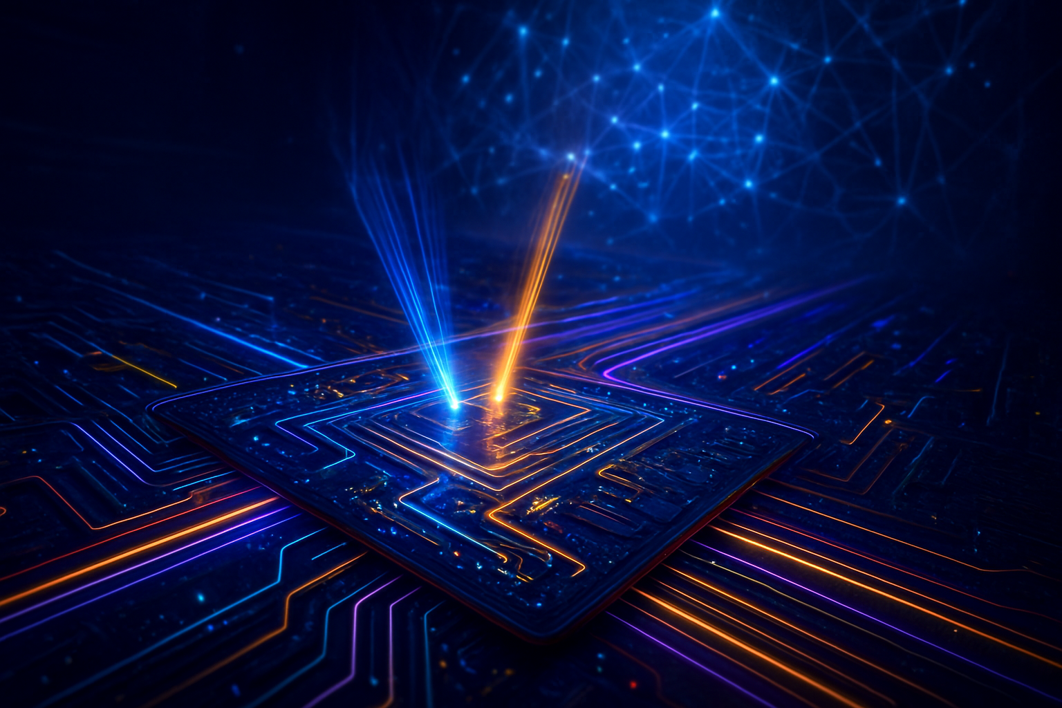
    The centerpiece of this technological shift is the "Photonic Fabric," a proprietary architecture developed by Celestial AI that Marvell is now integrating into its portfolio. Unlike traditional pluggable optics that sit at the edge of a motherboard, Celestial AI’s technology utilizes an Optical Multi-Chip Interconnect Bridge (OMIB). This allows for 3D packaging where optical interconnects are placed directly on the silicon substrate alongside AI accelerators (XPUs) and High Bandwidth Memory (HBM). By using light to transport data across these components, the Photonic Fabric delivers 25 times greater bandwidth while reducing latency and power consumption by a factor of ten compared to existing copper-based solutions.

    Broadcom (NASDAQ: AVGO) has simultaneously pushed the envelope with its own optical innovations, recently unveiling the Tomahawk 6 "Davidson" switch. This 102.4 Tbps Ethernet switch is the first to utilize 200G-per-lane Co-Packaged Optics (CPO). By integrating the optical engines directly into the switch package, Broadcom has slashed the energy required to move a bit of data, a feat previously thought impossible at these speeds. The industry's move to 1.6T and eventually 3.2T interconnects is now being realized through these advancements in silicon photonics, allowing hundreds of individual chips to function as a single, massive "virtual" processor.

    This shift represents a fundamental departure from the "scale-out" networking of the past decade. Previously, data centers connected clusters of servers using standard networking cables, which introduced significant lag. The new silicon photonics paradigm enables "scale-up" architectures, where the entire rack—or even multiple racks—is interconnected via a seamless web of light. This allows for near-instantaneous memory sharing across thousands of GPUs, effectively neutralizing the physical distance between chips and allowing larger models to be trained in a fraction of the time.

    Initial reactions from the AI research community have been overwhelmingly positive, with experts noting that these hardware breakthroughs are the "missing link" for trillion-parameter models. By moving the data bottleneck from the electrical domain to the optical domain, engineers can finally match the raw processing power of modern chips with a communication infrastructure that can keep up. The integration of 3nm Digital Signal Processors (DSPs) like Broadcom’s Sian3 further optimizes this ecosystem, ensuring that the transition to light is as power-efficient as possible.

    Market Dominance and the New Competitive Landscape

    The acquisition of Celestial AI positions Marvell Technology (NASDAQ: MRVL) as a formidable challenger to the established order of AI networking. By securing the Photonic Fabric technology, Marvell is targeting a $1 billion annualized revenue run rate for its optical business by 2029. This move is a direct shot across the bow of Nvidia (NASDAQ: NVDA) (NASDAQ: NVDA), which has traditionally dominated the AI interconnect space with its proprietary NVLink technology. Marvell’s strategy is to offer an open, high-performance alternative that appeals to hyperscalers like Google (NASDAQ: GOOGL) and Meta (NASDAQ: META), who are increasingly looking to decouple their hardware stacks from single-vendor ecosystems.

    Broadcom, meanwhile, has solidified its status as the "arms dealer" of the AI era. With AI revenue surging to $20 billion in 2025—a 65% year-over-year increase—Broadcom’s dominance in custom ASICs and high-end switching is unparalleled. Their record Q4 revenue of $6.5 billion was largely driven by the massive deployment of custom AI accelerators for major cloud providers. By leading the charge in Co-Packaged Optics, Broadcom is ensuring that it remains the primary partner for any firm building a massive AI cluster, effectively gatekeeping the physical layer of the AI revolution.

    The competitive implications for startups and smaller AI labs are profound. As the cost of building state-of-the-art optical infrastructure rises, the barrier to entry for training "frontier" models becomes even higher. However, the availability of standardized silicon photonics products from Marvell and Broadcom could eventually democratize access to high-performance interconnects, allowing smaller players to build more efficient clusters using off-the-shelf components rather than expensive, proprietary systems.

    For the tech giants, this development is a strategic win. Companies like Meta (NASDAQ: META) have already begun trialing Broadcom’s CPO solutions to lower the massive electricity bills associated with their AI data centers. As silicon photonics reduces the power overhead of data movement, these companies can allocate more of their power budget to actual computation, maximizing the return on their multi-billion dollar infrastructure investments. The market is now seeing a clear bifurcation: companies that master the integration of light and silicon will lead the next decade of AI, while those reliant on traditional copper interconnects risk being left in the dark.

    The Broader Significance: Sustaining the AI Boom

    The commercialization of silicon photonics is more than just a hardware upgrade; it is a vital survival mechanism for the AI industry. As the world grapples with the environmental impact of massive data centers, the energy efficiency gains provided by optical interconnects are essential. By reducing the power required for data transmission by 90%, silicon photonics offers a path toward sustainable AI scaling. This shift is critical as global power grids struggle to keep pace with the exponential demand for AI compute, turning energy efficiency into a competitive "moat" for the most advanced tech firms.

    This milestone also represents a significant extension of Moore’s Law. For years, skeptics argued that the end of traditional transistor scaling would lead to a plateau in computing performance. Silicon photonics bypasses this limitation by focusing on the "interconnect bottleneck" rather than just the raw transistor count. By improving the speed at which data moves between chips, the industry can continue to see massive performance gains even as individual processors face diminishing returns from further miniaturization.

    Comparisons are already being drawn to the transition from dial-up internet to fiber optics. Just as fiber optics revolutionized global communications by enabling the modern internet, silicon photonics is poised to do the same for internal computer architectures. This is the first time in the history of computing that optical technology has been integrated so deeply into the chip packaging itself, marking a permanent shift in how we design and build high-performance systems.

    However, the transition is not without concerns. The complexity of manufacturing silicon photonics at scale remains a significant challenge. The precision required to align laser sources with silicon waveguides is measured in nanometers, and any manufacturing defect can render an entire multi-thousand-dollar chip useless. Furthermore, the industry must now navigate a period of intense standardization, as different vendors vie to make their optical protocols the industry standard. The outcome of these "standards wars" will dictate the shape of the AI industry for the next twenty years.

    Future Horizons: From Data Centers to the Edge

    Looking ahead, the near-term focus will be the rollout of 1.6T and 3.2T optical networks throughout 2026 and 2027. Experts predict that the success of the Marvell-Celestial AI integration will trigger a wave of further consolidation in the semiconductor industry, as other players scramble to acquire optical IP. We are likely to see "optical-first" AI architectures where the processor and memory are no longer distinct units but are instead part of a unified, light-driven compute fabric.

    In the long term, the applications of silicon photonics could extend beyond the data center. While currently too expensive for consumer electronics, the maturation of the technology could eventually bring optical interconnects to high-end workstations and even specialized edge AI devices. This would enable "AI at the edge" with capabilities that currently require a cloud connection, such as real-time high-fidelity language translation or complex autonomous navigation, all while maintaining strict power efficiency.

    The next major challenge for the industry will be the integration of "on-chip" lasers. Currently, most silicon photonics systems rely on external laser sources, which adds complexity and potential points of failure. Research into integrating light-emitting materials directly into the silicon manufacturing process is ongoing, and a breakthrough in this area would represent the final piece of the silicon photonics puzzle. If successful, this would allow for truly monolithic optical chips, further driving down costs and increasing performance.

    A New Era of Luminous Computing

    The events of late 2025—Marvell’s multi-billion dollar bet on Celestial AI and Broadcom’s record-shattering AI revenue—will be remembered as the moment silicon photonics reached its commercial tipping point. The transition from copper to light is no longer a theoretical goal but a market reality that is reshaping the balance of power in the semiconductor industry. By solving the memory wall and drastically reducing power consumption, silicon photonics has provided the necessary foundation for the next decade of AI advancement.

    The key takeaway for the industry is that the "infrastructure bottleneck" is finally being broken. As light-based interconnects become standard, the focus will shift from how to move data to how to use it most effectively. This development is a testament to the ingenuity of the semiconductor community, which has successfully married the worlds of photonics and electronics to overcome the physical limits of traditional computing.

    In the coming weeks and months, investors and analysts will be closely watching the regulatory approval process for the Marvell-Celestial AI deal and Broadcom’s initial shipments of the Tomahawk 6 "Davidson" switch. These milestones will serve as the first real-world tests of the silicon photonics era. As the first light-driven AI clusters come online, the true potential of this technology will finally be revealed, ushering in a new age of luminous, high-efficiency computing.


    This content is intended for informational purposes only and represents analysis of current AI developments.

    TokenRing AI delivers enterprise-grade solutions for multi-agent AI workflow orchestration, AI-powered development tools, and seamless remote collaboration platforms.
    For more information, visit https://www.tokenring.ai/.

  • The Optical Revolution: Marvell’s $3.25B Celestial AI Acquisition and TSMC’s COUPE Bridge the AI Interconnect Gap

    The Optical Revolution: Marvell’s $3.25B Celestial AI Acquisition and TSMC’s COUPE Bridge the AI Interconnect Gap

    As the artificial intelligence industry grapples with the diminishing returns of traditional copper-based networking, a seismic shift toward silicon photonics has officially begun. In a landmark move on December 2, 2025, Marvell Technology (NASDAQ:MRVL) announced its definitive agreement to acquire Celestial AI for an upfront value of $3.25 billion. This acquisition, paired with the rapid commercialization of Taiwan Semiconductor Manufacturing Company’s (NYSE:TSM) Compact Universal Photonic Engine (COUPE) technology, marks the dawn of the "Optical Revolution" in AI hardware—a transition that replaces electrical signals with light to shatter the interconnect bottleneck.

    The immediate significance of these developments cannot be overstated. For years, the scaling of Large Language Models (LLMs) has been limited not just by raw compute power, but by the "Memory Wall" and the physical constraints of moving data between chips using copper wires. By integrating Celestial AI’s Photonic Fabric with TSMC’s advanced 3D packaging, the industry is moving toward a disaggregated architecture where memory and compute can be scaled independently. This shift is expected to reduce power consumption by over 50% while providing a 10x increase in bandwidth, effectively clearing the path for the next generation of models featuring tens of trillions of parameters.

    Breaking the Copper Ceiling: The Orion Platform and COUPE Integration

    At the heart of Marvell’s multi-billion dollar bet is Celestial AI’s Orion platform and its proprietary Photonic Fabric. Unlike traditional "scale-out" networking protocols like Ethernet or InfiniBand, which are designed for chip-to-chip communication over relatively long distances, the Photonic Fabric is a "scale-up" technology. It allows hundreds of XPUs—GPUs, CPUs, and custom accelerators—to be interconnected in multi-rack configurations with full memory coherence. This means that an entire data center rack can effectively function as a single, massive super-processor, with light-speed interconnects providing up to 16 terabits per second (Tbps) of bandwidth per link.

    TSMC’s COUPE technology provides the physical manufacturing vehicle for this optical future. COUPE utilizes TSMC’s SoIC-X (System on Integrated Chips) technology to stack an Electronic Integrated Circuit (EIC) directly on top of a Photonic Integrated Circuit (PIC) using "bumpless" copper-to-copper hybrid bonding. As of late 2025, TSMC has achieved a 6μm bond pitch, which drastically reduces electrical impedance and eliminates the need for power-hungry Digital Signal Processors (DSPs) to drive optical signals. This level of integration allows optical modulators to be placed directly on the 3nm silicon die, bypassing the "beachfront" limitations of traditional High-Bandwidth Memory (HBM).

    This approach differs fundamentally from previous pluggable optical transceivers. By bringing the optics "in-package"—a concept known as Co-Packaged Optics (CPO)—Marvell and TSMC are eliminating the energy-intensive step of converting signals from electrical to optical at the edge of the board. Initial reactions from the AI research community have been overwhelmingly positive, with experts noting that this architecture finally solves the "Stranded Memory" problem, where GPUs sit idle because they cannot access data fast enough from neighboring nodes.

    A New Competitive Landscape for AI Titans

    The acquisition of Celestial AI positions Marvell as a formidable challenger to Broadcom (NASDAQ:AVGO) and NVIDIA (NASDAQ:NVDA) in the high-stakes race for AI infrastructure dominance. By owning the full stack of optical interconnect IP, Marvell can now offer hyperscalers like Amazon (NASDAQ:AMZN) and Google a complete blueprint for next-generation AI factories. This move is particularly disruptive to the status quo because it offers a "memory-first" architecture that could potentially reduce the reliance on NVIDIA’s proprietary NVLink, giving cloud providers more flexibility in how they build their clusters.

    For NVIDIA, the pressure is on to integrate similar silicon photonics capabilities into its upcoming "Rubin" architecture. While NVIDIA remains the king of GPU compute, the battle is shifting toward who controls the "fabric" that connects those GPUs. TSMC’s COUPE technology serves as a neutral ground where major players, including Broadcom and Alchip (TWSE:3661), are already racing to validate their own 1.6T and 3.2T optical engines. The strategic advantage now lies with companies that can minimize the "energy-per-bit" cost of data movement, as power availability has become the primary bottleneck for data center expansion.

    Startups in the silicon photonics space are also seeing a massive valuation lift following the $3.25 billion Celestial AI deal. The market is signaling that "optical I/O" is no longer a research project but a production requirement. Companies that have spent the last decade perfecting micro-ring modulators and laser integration are now being courted by traditional semiconductor firms looking to avoid being left behind in the transition from electrons to photons.

    The Wider Significance: Scaling Toward the 100-Trillion Parameter Era

    The "Optical Revolution" fits into a broader trend of architectural disaggregation. For the past decade, AI scaling followed "Moore’s Law for Transistors," but we have now entered the era of "Moore’s Law for Interconnects." As models grow toward 100 trillion parameters, the energy required to move data across a data center using copper would exceed the power capacity of most municipal grids. Silicon photonics is the only viable path to maintaining the current trajectory of AI advancement without an exponential increase in carbon footprint.

    Comparing this to previous milestones, the shift to optical interconnects is as significant as the transition from CPUs to GPUs for deep learning. It represents a fundamental change in the physics of computing. However, this transition is not without concerns. The industry must now solve the challenge of "laser reliability," as thousands of external laser sources are required to power these optical fabrics. If a single laser fails, it could potentially take down an entire compute node, necessitating new redundancy protocols that the industry is still working to standardize.

    Furthermore, this development solidifies the role of advanced packaging as the new frontier of semiconductor innovation. The ability to stack optical engines directly onto logic chips means that the "foundry" is no longer just a place that etches transistors; it is a sophisticated assembly house where disparate materials and technologies are fused together. This reinforces the geopolitical importance of leaders like TSMC, whose COUPE and CoWoS-L platforms are now the bedrock of global AI progress.

    The Road Ahead: 12.8 Tbps and Beyond

    Looking toward the near-term, the first generation of COUPE-enabled 1.6 Tbps pluggable devices is expected to enter mass production in the second half of 2026. However, the true potential will be realized in 2027 and 2028 with the third generation of optical engines, which aim for a staggering 12.8 Tbps per engine. This will enable "Any-to-Any" memory access across thousands of GPUs with latencies low enough to treat remote HBM as if it were local to the processor.

    The potential applications extend beyond just training LLMs. Real-time AI video generation, complex climate modeling, and autonomous drug discovery all require the massive, low-latency memory pools that the Celestial AI acquisition makes possible. Experts predict that by 2030, the very concept of a "standalone server" will vanish, replaced by "Software-Defined Data Centers" where compute, memory, and storage are fluid resources connected by a persistent web of light.

    A Watershed Moment in AI History

    Marvell’s acquisition of Celestial AI and the arrival of TSMC’s COUPE technology will likely be remembered as the moment the "Copper Wall" was finally breached. By successfully replacing electrical signals with light at the chip level, the industry has secured a roadmap for AI scaling that can last through the end of the decade. This development isn't just an incremental improvement; it is a foundational shift in how we build the machines that think.

    As we move into 2026, the key metrics to watch will be the yield rates of TSMC’s bumpless bonding and the first real-world benchmarks of Marvell’s Orion-powered clusters. If these technologies deliver on their promise of 50% power savings, the "Optical Revolution" will not just be a technical triumph, but a critical component in making the AI-driven future economically and environmentally sustainable.


    This content is intended for informational purposes only and represents analysis of current AI developments.

    TokenRing AI delivers enterprise-grade solutions for multi-agent AI workflow orchestration, AI-powered development tools, and seamless remote collaboration platforms.
    For more information, visit https://www.tokenring.ai/.

  • Silicon Photonics: Moving AI Data at the Speed of Light

    Silicon Photonics: Moving AI Data at the Speed of Light

    As artificial intelligence models swell toward the 100-trillion-parameter mark, the industry has hit a physical wall: the "data traffic jam." Traditional copper-based networking and even standard optical transceivers are struggling to keep pace with the massive throughput required to synchronize thousands of GPUs in real-time. To solve this, the tech industry is undergoing a fundamental shift, moving from electrical signals to light-speed data transfer through the integration of silicon photonics directly onto silicon wafers.

    The emergence of silicon photonics marks a pivotal moment in the evolution of the "AI Factory." By embedding lasers and optical components into the same packages as processors and switches, companies are effectively removing the bottlenecks that have long plagued high-performance computing (HPC). Leading this charge is NVIDIA (NASDAQ: NVDA) with its Spectrum-X platform, which is redefining how data moves across the world’s most powerful AI clusters, enabling the next generation of generative AI models to train faster and more efficiently than ever before.

    The Light-Speed Revolution: Integrating Lasers on Silicon

    The technical breakthrough at the heart of this transition is the successful integration of lasers directly onto silicon wafers—a feat once considered the "Holy Grail" of semiconductor engineering. Historically, silicon is a poor emitter of light, necessitating external laser sources and bulky pluggable transceivers. However, by late 2025, heterogeneous integration—the process of bonding light-emitting materials like Indium Phosphide onto 300mm silicon wafers—has become a commercially viable reality. This allows for Co-Packaged Optics (CPO), where the optical engine sits in the same package as the switch silicon, drastically reducing the distance data must travel via electricity.

    NVIDIA’s Spectrum-X Ethernet Photonics platform is a prime example of this advancement. Unveiled as a cornerstone of the Blackwell-era networking stack, Spectrum-X now supports staggering switch throughputs of up to 400 Tbps in high-density configurations. By utilizing TSMC’s Compact Universal Photonic Engine (COUPE) technology, NVIDIA has 3D-stacked electronic and photonic circuits, eliminating the need for power-hungry Digital Signal Processors (DSPs). This architecture supports 1.6 Tbps per port, providing the massive bandwidth density required to feed trillion-parameter models without the latency spikes that typically derail large-scale training jobs.

    The shift to silicon photonics isn't just about speed; it's about resiliency. In traditional setups, "link flaps"—brief interruptions in data flow—are a common occurrence that can crash a training session involving 100,000 GPUs. Industry data suggests that silicon photonics-based networking, such as NVIDIA’s Quantum-X Photonics, offers up to 10x higher resiliency. This allows trillion-parameter model training to run for weeks without interruption, a necessity when the cost of a single training run can reach hundreds of millions of dollars.

    The Strategic Battle for the AI Backbone

    The move to silicon photonics has ignited a fierce competitive landscape among semiconductor giants and specialized startups. While NVIDIA (NASDAQ: NVDA) currently dominates the GPU-to-GPU interconnect market, Intel (NASDAQ: INTC) has positioned itself as a volume leader in integrated photonics. Having shipped over 32 million integrated lasers by the end of 2025, Intel is leveraging its "Optical Compute Interconnect" (OCI) chiplets to bridge the gap between CPUs, GPUs, and high-bandwidth memory, potentially challenging NVIDIA’s full-stack dominance in the data center.

    Broadcom (NASDAQ: AVGO) has also emerged as a heavyweight in this arena with its "Bailly" CPO switch series. By focusing on open standards and high-volume manufacturing, Broadcom is targeting hyperscalers who want to build massive AI clusters without being locked into a single vendor's ecosystem. Meanwhile, startups like Ayar Labs are playing a critical role; their TeraPHY™ optical I/O chiplets, which achieved 8 Tbps of bandwidth in recent 2025 trials, are being integrated by multiple partners to provide the high-speed "on-ramps" for optical data.

    This shift is disrupting the traditional transceiver market. Companies that once specialized in pluggable optical modules are finding themselves forced to pivot or partner with silicon foundries to stay relevant. For AI labs and tech giants, the strategic advantage now lies in who can most efficiently manage the "power-per-bit" ratio. Those who successfully implement silicon photonics can build larger clusters within the same power envelope, a critical factor as data centers begin to consume a double-digit percentage of the global energy supply.

    Scaling the Unscalable: Efficiency and the Future of AI Factories

    The broader significance of silicon photonics extends beyond raw performance; it is an environmental and economic necessity. As AI clusters scale toward millions of GPUs, the power consumption of traditional networking becomes unsustainable. Silicon photonics delivers approximately 3.5x better power efficiency compared to traditional pluggable transceivers. In a 400,000-GPU "AI Factory," switching to integrated optics can save tens of megawatts of power—enough to power a small city—while reducing total cluster power consumption by as much as 12%.

    This development fits into the larger trend of "computational convergence," where the network itself becomes part of the computer. With protocols like SHARPv4 (Scalable Hierarchical Aggregation and Reduction Protocol) integrated into photonic switches, the network can perform mathematical operations on data while it is in transit. This "in-network computing" offloads tasks from the GPUs, accelerating the convergence of 100-trillion-parameter models and reducing the overall time-to-solution.

    However, the transition is not without concerns. The complexity of 3D-stacking photonics and electronics introduces new challenges in thermal management and manufacturing yield. Furthermore, the industry is still debating the standards for optical interconnects, with various proprietary solutions competing for dominance. Comparisons are already being made to the transition from copper to fiber optics in the telecommunications industry decades ago—a shift that took years to fully mature but eventually became the foundation of the modern internet.

    Beyond the Rack: The Road to Optical Computing

    Looking ahead, the roadmap for silicon photonics suggests that we are only at the beginning of an "optical era." In the near term (2026-2027), we expect to see the first widespread deployments of 3.2 Tbps per port networking and the integration of optical I/O directly into the GPU die. This will effectively turn the entire data center into a single, massive "super-node," where the distance between two chips no longer dictates the speed of their communication.

    Potential applications extend into the realm of edge AI and autonomous systems, where low-latency, high-bandwidth communication is vital. Experts predict that as the cost of silicon photonics drops due to economies of scale, we may see optical interconnects appearing in consumer-grade hardware, enabling ultra-fast links between PCs and external AI accelerators. The ultimate goal remains "optical computing," where light is used not just to move data, but to perform the calculations themselves, potentially offering a thousand-fold increase in efficiency over electronic transistors.

    The immediate challenge remains the high-volume manufacturing of integrated lasers. While Intel and TSMC have made significant strides, achieving the yields necessary for global scale remains a hurdle. As the industry moves toward 200G-per-lane architectures, the precision required for optical alignment will push the boundaries of robotic assembly and semiconductor lithography.

    A New Era for AI Infrastructure

    The integration of silicon photonics into the AI stack represents one of the most significant infrastructure shifts in the history of computing. By moving data at the speed of light and integrating lasers directly onto silicon, the industry is effectively bypassing the physical limits of electricity. NVIDIA’s Spectrum-X and the innovations from Intel and Broadcom are not just incremental upgrades; they are the foundational technologies that will allow AI to scale to the next level of intelligence.

    The key takeaway for the industry is that the "data traffic jam" is finally clearing. As we move into 2026, the focus will shift from how many GPUs a company can buy to how efficiently they can connect them. Silicon photonics has become the prerequisite for any organization serious about training the 100-trillion-parameter models of the future.

    In the coming weeks and months, watch for announcements regarding the first live deployments of 1.6T CPO switches in hyperscale data centers. These early adopters will likely set the pace for the next wave of AI breakthroughs, proving that in the race for artificial intelligence, speed—quite literally—is everything.


    This content is intended for informational purposes only and represents analysis of current AI developments.

    TokenRing AI delivers enterprise-grade solutions for multi-agent AI workflow orchestration, AI-powered development tools, and seamless remote collaboration platforms.
    For more information, visit https://www.tokenring.ai/.

  • The Optical Revolution: Silicon Photonics Shatters the AI Interconnect Bottleneck

    The Optical Revolution: Silicon Photonics Shatters the AI Interconnect Bottleneck

    As of December 18, 2025, the artificial intelligence industry has reached a pivotal inflection point where the speed of light is no longer a theoretical limit, but a production requirement. For years, the industry has warned of a looming "interconnect bottleneck"—a physical wall where the electrical wires connecting GPUs could no longer keep pace with the massive data demands of trillion-parameter models. This week, that wall was officially dismantled as the tech industry fully embraced silicon photonics, shifting the fundamental medium of AI communication from electrons to photons.

    The significance of this transition cannot be overstated. With the recent announcement that Marvell Technology (NASDAQ: MRVL) has finalized its landmark acquisition of Celestial AI for $3.25 billion, the race to integrate "Photonic Fabrics" into the heart of AI silicon has moved from the laboratory to the center of the global supply chain. By replacing copper traces with microscopic lasers and fiber optics, AI clusters are now achieving bandwidth densities and energy efficiencies that were considered impossible just twenty-four months ago, effectively unlocking the next era of "cluster-scale" computing.

    The End of the Copper Era: Technical Breakthroughs in Optical I/O

    The primary driver behind the shift to silicon photonics is the dual crisis of the "Shoreline Limitation" and the "Power Wall." In traditional GPU architectures, such as the early iterations of the Blackwell series from Nvidia (NASDAQ: NVDA), data must travel through the physical edges (the shoreline) of the chip via electrical pins. As logic density increased, the perimeter of the chip simply ran out of room for more pins. Furthermore, pushing electrical signals through copper at speeds exceeding 200 Gbps requires massive amounts of power for signal retiming. In 2024, nearly 30% of an AI cluster's energy was wasted just moving data between chips; in late 2025, silicon photonics has slashed that "optics tax" by over 80%.

    Technically, this is achieved through Co-Packaged Optics (CPO) and Optical I/O chiplets. Instead of using external pluggable transceivers, companies are now 3D-stacking Photonic Integrated Circuits (PICs) directly onto the GPU or switch die. This allows for "Edgeless I/O," where data can be beamed directly from the center of the chip using light. Leading the charge is Broadcom (NASDAQ: AVGO), which recently began mass-shipping its Tomahawk 6 "Davidson" switch, the industry’s first 102.4 Tbps CPO platform. By integrating optical engines onto the substrate, Broadcom has reduced interconnect power consumption from 30 picojoules per bit (pJ/bit) to less than 5 pJ/bit.

    This shift differs fundamentally from previous networking upgrades. While past transitions moved from 400G to 800G using the same electrical principles, silicon photonics changes the physics of the connection. Startups like Lightmatter have introduced the Passage M1000, a photonic interposer that supports a staggering 114 Tbps of optical bandwidth. This "photonic superchip" allows thousands of individual accelerators to behave as a single, unified processor with near-zero latency, a feat the AI research community has hailed as the most significant hardware breakthrough since the invention of the High Bandwidth Memory (HBM) stack.

    Market Warfare: Who Wins the Photonic Arms Race?

    The competitive landscape of the semiconductor industry is being redrawn by this optical pivot. Nvidia remains the titan to beat, having integrated silicon photonics into its Rubin architecture, slated for wide release in 2026. By leveraging its Spectrum-X networking fabric, Nvidia is moving toward a future where the entire back-end of an AI supercomputer is a seamless web of light. However, the Marvell acquisition of Celestial AI signals a direct challenge to Nvidia’s dominance. Marvell’s new "Photonic Fabric" aims to provide an open, high-bandwidth alternative that allows third-party AI accelerators to compete with Nvidia’s proprietary NVLink on performance and scale.

    Broadcom and Intel (NASDAQ: INTC) are also carving out massive territories in this new market. Broadcom’s lead in CPO technology makes them the indispensable partner for "Hyperscalers" like Google and Meta, who are building custom AI silicon (XPUs) that require optical attaches to scale. Meanwhile, Intel has successfully integrated its Optical Compute Interconnect (OCI) chiplets into its latest Xeon and Gaudi lines. Intel’s milestone of shipping over 8 million PICs demonstrates a manufacturing maturity that many startups still struggle to match, positioning the company as a primary foundry for the photonic era.

    For AI startups and labs, this development is a strategic lifeline. The ability to scale clusters to 100,000+ GPUs without the exponential power costs of copper allows smaller players to train increasingly sophisticated models. However, the high capital expenditure required to transition to optical infrastructure may further consolidate power among the "Big Tech" firms that can afford to rebuild their data centers from the ground up. We are seeing a shift where the "moat" for an AI company is no longer just its algorithm, but the photonic efficiency of its underlying hardware fabric.

    Beyond the Bottleneck: Global and Societal Implications

    The broader significance of silicon photonics extends into the realm of global energy sustainability. As AI energy consumption became a flashpoint for environmental concerns in 2024 and 2025, the move to light-based communication offers a rare "green" win for the industry. By reducing the energy required for data movement by 5x to 10x, silicon photonics is the primary reason the tech industry can continue to scale AI capabilities without triggering a collapse of local power grids. It represents a decoupling of performance growth from energy growth.

    Furthermore, this technology is the key to achieving "Disaggregated Memory." In the electrical era, a GPU could only efficiently access the memory physically located on its board. With the low latency and long reach of light, 2025-era data centers are moving toward pools of memory that can be dynamically assigned to any processor in the rack. This "memory-centric" computing model is essential for the next generation of Large Multimodal Models (LMMs) that require petabytes of active memory to process real-time video and complex reasoning tasks.

    However, the transition is not without its concerns. The reliance on silicon photonics introduces new complexities in the supply chain, particularly regarding the manufacturing of high-reliability lasers. Unlike traditional silicon, these lasers are often made from III-V materials like Indium Phosphide, which are more difficult to integrate and have different failure modes. There is also a geopolitical dimension; as silicon photonics becomes the "secret sauce" of AI supremacy, export controls on photonic design software and manufacturing equipment are expected to tighten, mirroring the restrictions seen in the EUV lithography market.

    The Road Ahead: What’s Next for Optical Computing?

    Looking toward 2026 and 2027, the industry is already eyeing the next frontier: all-optical computing. While silicon photonics currently handles the communication between chips, companies like Ayar Labs and Lightmatter are researching ways to perform certain computations using light itself. This would involve optical matrix-vector multipliers that could process neural network layers at the speed of light with almost zero heat generation. While still in the early stages, the success of optical I/O has provided the commercial foundation for these more radical architectures.

    In the near term, expect to see the "UCIe (Universal Chiplet Interconnect Express) over Light" standard become the dominant protocol for chip-to-chip communication. This will allow a "Lego-like" ecosystem where a customer can pair an Nvidia GPU with a Marvell photonic chiplet and an Intel memory controller, all communicating over a standardized optical bus. The main challenge remains the "yield" of these complex 3D-stacked packages; as manufacturing processes mature throughout 2026, we expect the cost of optical I/O to drop, eventually making it standard even in consumer-grade edge AI devices.

    Experts predict that by 2028, the term "interconnect bottleneck" will be a relic of the past. The focus will shift from how to move data to how to manage the sheer volume of intelligence that these light-speed clusters can generate. The "Optical Era" of AI is not just about faster chips; it is about the creation of a global, light-based neural fabric that can sustain the computational demands of Artificial General Intelligence (AGI).

    A New Foundation for the Intelligence Age

    The transition to silicon photonics marks the end of the "Electrical Bottleneck" that has constrained computer architecture since the 1940s. By successfully replacing copper with light, the AI industry has bypassed a physical limit that many feared would stall the progress of machine intelligence. The developments we have witnessed in late 2025—from Marvell’s strategic acquisitions to Broadcom’s record-breaking switches—confirm that the future of AI is optical.

    As we look forward, the significance of this milestone will likely be compared to the transition from vacuum tubes to transistors. It is a fundamental shift in the physics of information. While the challenges of laser reliability and manufacturing costs remain, the momentum is irreversible. For the coming months, keep a close watch on the deployment of "Rubin" systems and the first wave of 100-Tbps optical switches; these will be the yardsticks by which we measure the success of the photonic revolution.


    This content is intended for informational purposes only and represents analysis of current AI developments.

    TokenRing AI delivers enterprise-grade solutions for multi-agent AI workflow orchestration, AI-powered development tools, and seamless remote collaboration platforms.
    For more information, visit https://www.tokenring.ai/.

  • The Light-Speed Revolution: Co-Packaged Optics and the Future of AI Clusters

    The Light-Speed Revolution: Co-Packaged Optics and the Future of AI Clusters

    As of December 18, 2025, the artificial intelligence industry has reached a critical inflection point where the physical limits of electricity are no longer sufficient to sustain the exponential growth of large language models. For years, AI clusters relied on traditional copper wiring and pluggable optical modules to move data between processors. However, as clusters scale toward the "mega-datacenter" level—housing upwards of one million accelerators—the "power wall" of electrical interconnects has become a primary bottleneck. The solution that has officially moved from the laboratory to the production line this year is Co-Packaged Optics (CPO) and Photonic Interconnects, a paradigm shift that replaces electrical signaling with light directly at the chip level.

    This transition marks the most significant architectural change in data center networking in over a decade. By integrating optical engines directly onto the same package as the AI accelerator or switch silicon, CPO eliminates the energy-intensive process of driving electrical signals across printed circuit boards. The immediate significance is staggering: a massive reduction in the "optics tax"—the percentage of a data center's power budget consumed purely by moving data rather than processing it. In 2025, the industry has witnessed the first large-scale deployments of these technologies, enabling AI clusters to maintain the scaling laws that have defined the generative AI era.

    The Technical Shift: From Pluggable Modules to Photonic Chiplets

    The technical leap from traditional pluggable optics to CPO is defined by two critical metrics: bandwidth density and energy efficiency. Traditional pluggable modules, while convenient, require power-hungry Digital Signal Processors (DSPs) to maintain signal integrity over the distance from the chip to the edge of the rack. In contrast, 2025-era CPO solutions, such as those standardized by the Optical Internetworking Forum (OIF), achieve a "shoreline" bandwidth density of 1.0 to 2.0 Terabits per second per millimeter (Tbps/mm). This is a nearly tenfold improvement over the 0.1 Tbps/mm limit of copper-based SerDes, allowing for vastly more data to enter and exit a single chip package.

    Furthermore, the energy efficiency of these photonic interconnects has finally broken the 5 picojoules per bit (pJ/bit) barrier, with some specialized "optical chiplets" approaching sub-1 pJ/bit performance. This is a radical departure from the 15-20 pJ/bit required by 800G or 1.6T pluggable optics. To address the historical concern of laser reliability—where a single laser failure could take down an entire $40,000 GPU—the industry has moved toward the External Laser Small Form Factor Pluggable (ELSFP) standard. This architecture keeps the laser source as a field-replaceable unit on the front panel, while the photonic engine remains co-packaged with the ASIC, ensuring high uptime and serviceability for massive AI fabrics.

    Initial reactions from the AI research community have been overwhelmingly positive, particularly among those working on "scale-out" architectures. Experts at the 2025 Optical Fiber Communication (OFC) conference noted that without CPO, the latency introduced by traditional networking would have eventually collapsed the training efficiency of models with tens of trillions of parameters. By utilizing "Linear Drive" architectures and eliminating the latency of complex error correction and DSPs, CPO provides the ultra-low latency required for the next generation of synchronous AI training.

    The Market Landscape: Silicon Giants and Photonic Disruptors

    The shift to light-based data movement has created a new hierarchy among tech giants and hardware manufacturers. Broadcom (NASDAQ: AVGO) has solidified its lead in this space with the wide-scale sampling of its third-generation Bailly-series CPO-integrated switches. These 102.4T switches are the first to demonstrate that CPO can be manufactured at scale with high yields. Similarly, NVIDIA (NASDAQ: NVDA) has integrated CPO into its Spectrum-X800 and Quantum-X800 platforms, confirming that its upcoming "Rubin" architecture will rely on optical chiplets to extend the reach of NVLink across entire data centers, effectively turning thousands of GPUs into a single, giant "Virtual GPU."

    Marvell Technology (NASDAQ: MRVL) has also emerged as a powerhouse, integrating its 6.4 Tbps silicon-photonic engines into custom AI ASICs for hyperscalers. The market positioning of these companies has shifted from selling "chips" to selling "integrated photonic platforms." Meanwhile, Intel (NASDAQ: INTC) has pivoted its strategy toward providing the foundational glass substrates and "Through-Glass Via" (TGV) technology necessary for the high-precision packaging that CPO demands. This strategic move allows Intel to benefit from the growth of the entire CPO ecosystem, even as competitors lead in the design of the optical engines themselves.

    The competitive implications are profound for AI labs like those at Meta (NASDAQ: META) and Microsoft (NASDAQ: MSFT). These companies are no longer just customers of hardware; they are increasingly co-designing the photonic fabrics that connect their proprietary AI accelerators. The disruption to existing services is most visible in the traditional pluggable module market, where vendors who failed to transition to silicon photonics are finding themselves sidelined in the high-end AI market. The strategic advantage now lies with those who control the "optical I/O," as this has become the primary constraint on AI training speed.

    Wider Significance: Sustaining the AI Scaling Laws

    Beyond the immediate technical and corporate gains, the rise of CPO is essential for the broader AI landscape's sustainability. The energy consumption of AI data centers has become a global concern, and the "optics tax" was on a trajectory to consume nearly half of a cluster's power by 2026. By slashing the energy required for data movement by 70% or more, CPO provides a temporary reprieve from the energy crisis facing the industry. This fits into the broader trend of "efficiency-led scaling," where breakthroughs are no longer just about more transistors, but about more efficient communication between them.

    However, this transition is not without concerns. The complexity of manufacturing co-packaged optics is significantly higher than traditional electronic packaging. There are also geopolitical implications, as the supply chain for silicon photonics is highly specialized. While Western firms like Broadcom and NVIDIA lead in design, Chinese manufacturers like InnoLight have made massive strides in high-volume CPO assembly, creating a bifurcated market. Comparisons are already being made to the "EUV moment" in lithography—a critical, high-barrier technology that separates the leaders from the laggards in the global tech race.

    This milestone is comparable to the introduction of High Bandwidth Memory (HBM) in the mid-2010s. Just as HBM solved the "memory wall" by bringing memory closer to the processor, CPO is solving the "interconnect wall" by bringing the network directly onto the chip package. It represents a fundamental shift in how we think about computers: no longer as a collection of separate boxes connected by wires, but as a unified, light-speed fabric of compute and memory.

    The Horizon: Optical Computing and Memory Disaggregation

    Looking toward 2026 and beyond, the integration of CPO is expected to enable even more radical architectures. One of the most anticipated developments is "Memory Disaggregation," where pools of HBM are no longer tied to a specific GPU but are accessible via a photonic fabric to any processor in the cluster. This would allow for much more flexible resource allocation and could drastically reduce the cost of running large-scale inference workloads. Startups like Celestial AI are already demonstrating "Photonic Fabric" architectures that treat memory and compute as a single, fluid pool connected by light.

    Challenges remain, particularly in the standardization of the software stack required to manage these optical networks. Experts predict that the next two years will see a "software-defined optics" revolution, where the network topology can be reconfigured in real-time using Optical Circuit Switching (OCS), similar to the Apollo system pioneered by Alphabet (NASDAQ: GOOGL). This would allow AI clusters to physically change their wiring to match the specific requirements of a training algorithm, further optimizing performance.

    In the long term, the lessons learned from CPO may pave the way for true optical computing, where light is used not just to move data, but to perform calculations. While this remains a distant goal, the successful commercialization of photonic interconnects in 2025 has proven that silicon photonics can be manufactured at the scale and reliability required by the world's most demanding applications.

    Summary and Final Thoughts

    The emergence of Co-Packaged Optics and Photonic Interconnects as a mainstream technology in late 2025 marks the end of the "Copper Era" for high-performance AI. By integrating light-speed communication directly into the heart of the silicon package, the industry has overcome a major physical barrier to scaling AI clusters. The key takeaways are clear: CPO is no longer a luxury but a necessity for the 1.6T and 3.2T networking eras, offering massive improvements in energy efficiency, bandwidth density, and latency.

    This development will likely be remembered as the moment when the "physicality" of the internet finally caught up with the "virtuality" of AI. As we move into 2026, the industry will be watching for the first "all-optical" AI data centers and the continued evolution of the ELSFP standards. For now, the transition to light-based data movement has ensured that the scaling laws of AI can continue, at least for a few more generations, as we continue the quest for ever-more powerful and efficient artificial intelligence.


    This content is intended for informational purposes only and represents analysis of current AI developments.

    TokenRing AI delivers enterprise-grade solutions for multi-agent AI workflow orchestration, AI-powered development tools, and seamless remote collaboration platforms.
    For more information, visit https://www.tokenring.ai/.

  • The Dawn of Hyper-Intelligent AI: Semiconductor Breakthroughs Forge a New Era of Integrated Processing

    The Dawn of Hyper-Intelligent AI: Semiconductor Breakthroughs Forge a New Era of Integrated Processing

    The landscape of artificial intelligence is undergoing a profound transformation, fueled by unprecedented breakthroughs in semiconductor manufacturing and chip integration. These advancements are not merely incremental improvements but represent a fundamental shift in how AI hardware is designed and built, promising to unlock new levels of performance, efficiency, and capability. At the heart of this revolution are innovations in neuromorphic computing, advanced packaging, and specialized process technologies, with companies like Tower Semiconductor (NASDAQ: TSEM) playing a critical role in shaping the future of AI.

    This new wave of silicon innovation is directly addressing the escalating demands of increasingly complex AI models, particularly large language models and sophisticated edge AI applications. By overcoming traditional bottlenecks in data movement and processing, these integrated solutions are paving the way for a generation of AI that is not only faster and more powerful but also significantly more energy-efficient and adaptable, pushing the boundaries of what intelligent machines can achieve.

    Engineering Intelligence: A Deep Dive into the Technical Revolution

    The technical underpinnings of this AI hardware revolution are multifaceted, spanning novel architectures, advanced materials, and sophisticated manufacturing techniques. One of the most significant shifts is the move towards Neuromorphic Computing and In-Memory Computing (IMC), which seeks to emulate the human brain's integrated processing and memory. Researchers at MIT, for instance, have engineered a "brain on a chip" using tens of thousands of memristors made from silicone and silver-copper alloys. These memristors exhibit enhanced conductivity and reliability, performing complex operations like image recognition directly within the memory unit, effectively bypassing the "von Neumann bottleneck" that plagues conventional architectures. Similarly, Stanford University and UC San Diego engineers developed NeuRRAM, a compute-in-memory (CIM) chip utilizing resistive random-access memory (RRAM), demonstrating AI processing directly in memory with accuracy comparable to digital chips but with vastly improved energy efficiency, ideal for low-power edge devices. Further innovations include Professor Hussam Amrouch at TUM's AI chip with Ferroelectric Field-Effect Transistors (FeFETs) for in-memory computing, and IBM Research's advancements in 3D analog in-memory architecture with phase-change memory, proving uniquely suited for running cutting-edge Mixture of Experts (MoE) models.

    Beyond brain-inspired designs, Advanced Packaging Technologies are crucial for overcoming the physical and economic limits of traditional monolithic chip scaling. The modular chiplet approach, where smaller, specialized components (logic, memory, RF, photonics, sensors) are interconnected within a single package, offers unprecedented scalability and flexibility. Standards like UCIe™ (Universal Chiplet Interconnect Express) are vital for ensuring interoperability. Hybrid Bonding, a cutting-edge technique, directly connects metal pads on semiconductor devices at a molecular level, achieving significantly higher interconnect density and reduced power consumption. Applied Materials introduced the Kinex system, the industry's first integrated die-to-wafer hybrid bonding platform, targeting high-performance logic and memory. Graphcore's Bow Intelligence Processing Unit (BOW), for example, is the world's first 3D Wafer-on-Wafer (WoW) processor, leveraging TSMC's 3D SoIC technology to boost AI performance by up to 40%. Concurrently, Gate-All-Around (GAA) Transistors, supported by systems like Applied Materials' Centura Xtera Epi, are enhancing transistor performance at the 2nm node and beyond, offering superior gate control and reduced leakage.

    Crucially, Silicon Photonics (SiPho) is emerging as a cornerstone technology. By transmitting data using light instead of electrical signals, SiPho enables significantly higher speeds and lower power consumption, addressing the bandwidth bottleneck in data centers and AI accelerators. This fundamental shift from electrical to optical interconnects within and between chips is paramount for scaling future AI systems. The initial reaction from the AI research community and industry experts has been overwhelmingly positive, recognizing these integrated approaches as essential for sustaining the rapid pace of AI innovation. They represent a departure from simply shrinking transistors, moving towards architectural and packaging innovations that deliver step-function improvements in AI capability.

    Reshaping the AI Ecosystem: Winners, Disruptors, and Strategic Advantages

    These breakthroughs are profoundly reshaping the competitive landscape for AI companies, tech giants, and startups alike. Companies that can effectively leverage these integrated chip solutions stand to gain significant competitive advantages. Hyperscale cloud providers and AI infrastructure developers are prime beneficiaries, as the dramatic increases in performance and energy efficiency directly translate to lower operational costs and the ability to deploy more powerful AI services. Companies specializing in edge AI, such as those developing autonomous vehicles, smart wearables, and IoT devices, will also see immense benefits from the reduced power consumption and smaller form factors offered by neuromorphic and in-memory computing chips.

    The competitive implications are substantial. Major AI labs and tech companies are now in a race to integrate these advanced hardware capabilities into their AI stacks. Those with strong in-house chip design capabilities, like NVIDIA (NASDAQ: NVDA), Intel (NASDAQ: INTC), and Google (NASDAQ: GOOGL), are pushing their own custom accelerators and integrated solutions. However, the rise of specialized foundries and packaging experts creates opportunities for disruption. Traditional CPU/GPU-centric approaches might face increasing competition from highly specialized, integrated AI accelerators tailored for specific workloads, potentially disrupting existing product lines for general-purpose processors.

    Tower Semiconductor (NASDAQ: TSEM), as a global specialty foundry, exemplifies a company strategically positioned to capitalize on these trends. Rather than focusing on leading-edge logic node shrinkage, Tower excels in customized analog solutions and specialty process technologies, particularly in Silicon Photonics (SiPho) and Silicon-Germanium (SiGe). These technologies are critical for high-speed optical data transmission and improved performance in AI and data center networks. Tower is investing $300 million to expand SiPho and SiGe chip production across its global fabrication plants, demonstrating its commitment to this high-growth area. Furthermore, their collaboration with partners like OpenLight and their focus on advanced power management solutions, such as the SW2001 buck regulator developed with Switch Semiconductor for AI compute systems, cement their role as a vital enabler for next-generation AI infrastructure. By securing capacity at an Intel fab and transferring its advanced power management flows, Tower is also leveraging strategic partnerships to expand its reach and capabilities, becoming an Intel Foundry customer while maintaining its specialized technology focus. This strategic focus provides Tower with a unique market positioning, offering essential components that complement the offerings of larger, more generalized chip manufacturers.

    The Wider Significance: A Paradigm Shift for AI

    These semiconductor breakthroughs represent more than just technical milestones; they signify a paradigm shift in the broader AI landscape. They are directly enabling the continued exponential growth of AI models, particularly Large Language Models (LLMs), by providing the necessary hardware to train and deploy them more efficiently. The advancements fit perfectly into the trend of increasing computational demands for AI, offering solutions that go beyond simply scaling up existing architectures.

    The impacts are far-reaching. Energy efficiency is dramatically improved, which is critical for both environmental sustainability and the widespread deployment of AI at the edge. Scalability and customization through chiplets allow for highly optimized hardware tailored to diverse AI workloads, accelerating innovation and reducing design cycles. Smaller form factors and increased data privacy (by enabling more local processing) are also significant benefits. These developments push AI closer to ubiquitous integration into daily life, from advanced robotics and autonomous systems to personalized intelligent assistants.

    While the benefits are immense, potential concerns exist. The complexity of designing and manufacturing these highly integrated systems is escalating, posing challenges for yield rates and overall cost. Standardization, especially for chiplet interconnects (e.g., UCIe), is crucial but still evolving. Nevertheless, when compared to previous AI milestones, such as the introduction of powerful GPUs that democratized deep learning, these current breakthroughs represent a deeper, architectural transformation. They are not just making existing AI faster but enabling entirely new classes of AI systems that were previously impractical due due to power or performance constraints.

    The Horizon of Hyper-Integrated AI: What Comes Next

    Looking ahead, the trajectory of AI hardware development points towards even greater integration and specialization. In the near-term, we can expect continued refinement and widespread adoption of existing advanced packaging techniques like hybrid bonding and chiplets, with an emphasis on improving interconnect density and reducing latency. The standardization efforts around interfaces like UCIe will be critical for fostering a more robust and interoperable chiplet ecosystem, allowing for greater innovation and competition.

    Long-term, experts predict a future dominated by highly specialized, domain-specific AI accelerators, often incorporating neuromorphic and in-memory computing principles. The goal is to move towards true "AI-native" hardware that fundamentally rethinks computation for neural networks. Potential applications are vast, including hyper-efficient generative AI models running on personal devices, fully autonomous robots with real-time decision-making capabilities, and sophisticated medical diagnostics integrated directly into wearable sensors.

    However, significant challenges remain. Overcoming the thermal management issues associated with 3D stacking, reducing the cost of advanced packaging, and developing robust design automation tools for heterogeneous integration are paramount. Furthermore, the software stack will need to evolve rapidly to fully exploit the capabilities of these novel hardware architectures, requiring new programming models and compilers. Experts predict a future where AI hardware becomes increasingly indistinguishable from the AI itself, with self-optimizing and self-healing systems. The next few years will likely see a proliferation of highly customized AI processing units, moving beyond the current CPU/GPU dichotomy to a more diverse and specialized hardware landscape.

    A New Epoch for Artificial Intelligence: The Integrated Future

    In summary, the recent breakthroughs in AI and advanced chip integration are ushering in a new epoch for artificial intelligence. From the brain-inspired architectures of neuromorphic computing to the modularity of chiplets and the speed of silicon photonics, these innovations are fundamentally reshaping the capabilities and efficiency of AI hardware. They address the critical bottlenecks of data movement and power consumption, enabling AI models to grow in complexity and deploy across an ever-wider array of applications, from cloud to edge.

    The significance of these developments in AI history cannot be overstated. They represent a pivotal moment where hardware innovation is directly driving the next wave of AI advancements, moving beyond the limits of traditional scaling. Companies like Tower Semiconductor (NASDAQ: TSEM), with their specialized expertise in areas like silicon photonics and power management, are crucial enablers in this transformation, providing the foundational technologies that empower the broader AI ecosystem.

    In the coming weeks and months, we should watch for continued announcements regarding new chip architectures, further advancements in packaging technologies, and expanding collaborations between chip designers, foundries, and AI developers. The race to build the most efficient and powerful AI hardware is intensifying, promising an exciting and transformative future where artificial intelligence becomes even more intelligent, pervasive, and impactful.


    This content is intended for informational purposes only and represents analysis of current AI developments.

    TokenRing AI delivers enterprise-grade solutions for multi-agent AI workflow orchestration, AI-powered development tools, and seamless remote collaboration platforms.
    For more information, visit https://www.tokenring.ai/.

  • The AI Chip Revolution: New Semiconductor Tech Unlocks Unprecedented Performance for AI and HPC

    The AI Chip Revolution: New Semiconductor Tech Unlocks Unprecedented Performance for AI and HPC

    As of late 2025, the semiconductor industry is undergoing a monumental transformation, driven by the insatiable demands of Artificial Intelligence (AI) and High-Performance Computing (HPC). This period marks not merely an evolution but a paradigm shift, where specialized architectures, advanced integration techniques, and novel materials are converging to deliver unprecedented levels of performance, energy efficiency, and scalability. These breakthroughs are immediately significant, enabling the development of far more complex AI models, accelerating scientific discovery across numerous fields, and powering the next generation of data centers and edge devices.

    The relentless pursuit of computational power and data throughput for AI workloads, particularly for large language models (LLMs) and real-time inference, has pushed the boundaries of traditional chip design. The advancements observed are critical for overcoming the physical limitations of Moore's Law, paving the way for a future where intelligent systems are more pervasive and powerful than ever imagined. This intense innovation is reshaping the competitive landscape, with major players and startups alike vying to deliver the foundational hardware for the AI-driven future.

    Beyond the Silicon Frontier: Technical Deep Dive into AI/HPC Semiconductor Advancements

    The current wave of semiconductor innovation for AI and HPC is characterized by several key technical advancements, moving beyond simple transistor scaling to embrace holistic system-level optimization.

    One of the most impactful shifts is in Advanced Packaging and Heterogeneous Integration. Traditional 2D chip design is giving way to 2.5D and 3D stacking technologies, where multiple dies are integrated within a single package. This includes placing chips side-by-side on an interposer (2.5D) or vertically stacking them (3D) using techniques like hybrid bonding. This approach dramatically improves communication between components, reduces energy consumption, and boosts overall efficiency. Chiplet architectures further exemplify this trend, allowing modular components (CPUs, GPUs, memory, accelerators) to be combined flexibly, optimizing process node utilization and functionality while reducing power. Companies like Taiwan Semiconductor Manufacturing Company (TSMC: TPE: 2330), Samsung Electronics (KRX: 005930), and Intel Corporation (NASDAQ: INTC) are at the forefront of these packaging innovations. For instance, Synopsys (NASDAQ: SNPS) predicts that 50% of new HPC chip designs will adopt 2.5D or 3D multi-die approaches by 2025. Emerging technologies like Fan-Out Panel-Level Packaging (FO-PLP) and the use of glass substrates are also gaining traction, offering superior dimensional stability and cost efficiency for complex AI/HPC engine architectures.

    Beyond general-purpose processors, Specialized AI and HPC Architectures are becoming mainstream. Custom AI accelerators such as Neural Processing Units (NPUs), Tensor Processing Units (TPUs), and Domain-Specific Accelerators (DSAs) are meticulously optimized for neural networks and machine learning, particularly for the demanding requirements of LLMs. By 2025, AI inference workloads are projected to surpass AI training, driving significant demand for hardware capable of real-time, energy-efficient processing. A fascinating development is Neuromorphic Computing, which emulates the human brain's neural networks in silicon. These chips, like those from BrainChip (ASX: BRN) (Akida), Intel (Loihi 2), and IBM (NYSE: IBM) (TrueNorth), are moving from academic research to commercial viability, offering significant advancements in processing power and energy efficiency (up to 80% less than conventional AI systems) for ultra-low power edge intelligence.

    Memory Innovations are equally critical to address the massive data demands. High-Bandwidth Memory (HBM), specifically HBM3, HBM3e, and the anticipated HBM4 (expected in late 2025), is indispensable for AI accelerators and HPC due to its exceptional data transfer rates, reduced latency, and improved computational efficiency. The memory segment is projected to grow over 24% in 2025, with HBM leading the surge. Furthermore, In-Memory Computing (CIM) is an emerging paradigm that integrates computation directly within memory, aiming to circumvent the "memory wall" bottleneck and significantly reduce latency and power consumption for AI workloads.

    To handle the immense data flow, Advanced Interconnects are crucial. Silicon Photonics and Co-Packaged Optics (CPO) are revolutionizing connectivity by integrating optical modules directly within the chip package. This offers increased bandwidth, superior signal integrity, longer reach, and enhanced resilience compared to traditional copper interconnects. NVIDIA Corporation (NASDAQ: NVDA) has announced new networking switch platforms, Spectrum-X Photonics and Quantum-X Photonics, based on CPO technology, with Quantum-X scheduled for late 2025, incorporating TSMC's 3D hybrid bonding. Advanced Micro Devices (AMD: NASDAQ: AMD) is also pushing the envelope with its high-speed SerDes for EPYC CPUs and Instinct GPUs, supporting future PCIe 6.0/7.0, and evolving its Infinity Fabric to Gen5 for unified compute across heterogeneous systems. The upcoming Ultra Ethernet specification and next-generation electrical interfaces like CEI-448G are also set to redefine HPC and AI networks with features like packet trimming and scalable encryption.

    Finally, continuous innovation in Manufacturing Processes and Materials underpins all these advancements. Leading-edge CPUs are now utilizing 3nm technology, with 2nm expected to enter mass production in 2025 by TSMC, Samsung, and Intel. Gate-All-Around (GAA) transistors are becoming widespread for improved gate control at smaller nodes, and High-Numerical Aperture (High-NA) Extreme Ultraviolet (EUV) Lithography is essential for precision. Interestingly, AI itself is being employed to design new functional materials, particularly compound semiconductors, promising enhanced performance and energy efficiency for HPC.

    Shifting Sands: How New Semiconductor Tech Reshapes the AI Industry Landscape

    The emergence of these advanced semiconductor technologies is profoundly impacting the competitive dynamics among AI companies, tech giants, and startups, creating both immense opportunities and potential disruptions.

    NVIDIA Corporation (NASDAQ: NVDA), already a dominant force in AI hardware with its GPUs, stands to significantly benefit from the continued demand for high-performance computing and its investments in advanced interconnects like CPO. Its strategic focus on a full-stack approach, encompassing hardware, software, and networking, positions it strongly. However, the rise of specialized accelerators and chiplet architectures could also open avenues for competitors. Advanced Micro Devices (AMD: NASDAQ: AMD) is aggressively expanding its presence in the AI and HPC markets with its EPYC CPUs and Instinct GPUs, coupled with its Infinity Fabric technology. By focusing on open standards and a broader ecosystem, AMD aims to capture a larger share of the burgeoning market.

    Major tech giants like Google (NASDAQ: GOOGL), with its Tensor Processing Units (TPUs), and Amazon (NASDAQ: AMZN), with its custom Trainium and Inferentia chips, are leveraging their internal hardware development capabilities to optimize their cloud AI services. This vertical integration allows them to offer highly efficient and cost-effective solutions tailored to their specific AI workloads, potentially disrupting traditional hardware vendors. Intel Corporation (NASDAQ: INTC), while facing stiff competition, is making a strong comeback with its foundry services and investments in advanced packaging, neuromorphic computing (Loihi 2), and next-generation process nodes, aiming to regain its leadership position in foundational silicon.

    Startups specializing in specific AI acceleration, such as those developing novel neuromorphic chips or in-memory computing solutions, stand to gain significant market traction. These smaller, agile companies can innovate rapidly in niche areas, potentially being acquired by larger players or establishing themselves as key component providers. The shift towards chiplet architectures also democratizes chip design to some extent, allowing smaller firms to integrate specialized IP without the prohibitive costs of designing an entire SoC from scratch. This could foster a more diverse ecosystem of AI hardware providers.

    The competitive implications are clear: companies that can rapidly adopt and integrate these new technologies will gain significant strategic advantages. Those heavily invested in older architectures or lacking the R&D capabilities to innovate in packaging, specialized accelerators, or memory will face increasing pressure. The market is increasingly valuing system-level integration and energy efficiency, making these critical differentiators. Furthermore, the geopolitical and supply chain dynamics, particularly concerning manufacturing leaders like TSMC (TPE: 2330) and Samsung (KRX: 005930), mean that securing access to leading-edge foundry services and advanced packaging capacity is a strategic imperative for all players.

    The Broader Canvas: Significance in the AI Landscape and Beyond

    These advancements in semiconductor technology are not isolated incidents; they represent a fundamental reshaping of the broader AI landscape and trends, with far-reaching implications for society, technology, and even global dynamics.

    Firstly, the relentless drive for energy efficiency in these new chips is a critical response to the immense power demands of AI-driven data centers. As AI models grow exponentially in size and complexity, their carbon footprint becomes a significant concern. Innovations in advanced cooling solutions like microfluidic and liquid cooling, alongside intrinsically more efficient chip designs, are essential for sustainable AI growth. This focus aligns with global efforts to combat climate change and will likely influence the geographic distribution and design of future data centers.

    Secondly, the rise of specialized AI accelerators and neuromorphic computing signifies a move beyond general-purpose computing for AI. This trend allows for hyper-optimization of specific AI tasks, leading to breakthroughs in areas like real-time computer vision, natural language processing, and autonomous systems that were previously computationally prohibitive. The commercial viability of neuromorphic chips by 2025, for example, marks a significant milestone, potentially enabling ultra-low-power edge AI applications from smart sensors to advanced robotics. This could democratize AI access by bringing powerful inferencing capabilities to devices with limited power budgets.

    The emphasis on system-level integration and co-packaged optics signals a departure from the traditional focus solely on transistor density. The "memory wall" and data movement bottlenecks have become as critical as processing power. By integrating memory and optical interconnects directly into the chip package, these technologies are breaking down historical barriers, allowing for unprecedented data throughput and reduced latency. This will accelerate scientific discovery in fields requiring massive data processing, such as genomics, materials science, and climate modeling, by enabling faster simulations and analysis.

    Potential concerns, however, include the increasing complexity and cost of developing and manufacturing these cutting-edge chips. The capital expenditure required for advanced foundries and R&D can be astronomical, potentially leading to further consolidation in the semiconductor industry and creating higher barriers to entry for new players. Furthermore, the reliance on a few key manufacturing hubs, predominantly in Asia-Pacific, continues to raise geopolitical and supply chain concerns, highlighting the strategic importance of semiconductor independence for major nations.

    Compared to previous AI milestones, such as the advent of deep learning or the transformer architecture, these semiconductor advancements represent the foundational infrastructure that enables the next generation of algorithmic breakthroughs. Without these hardware innovations, the computational demands of future AI models would be insurmountable. They are not just enhancing existing capabilities; they are creating the conditions for entirely new possibilities in AI, pushing the boundaries of what machines can learn and achieve.

    The Road Ahead: Future Developments and Predictions

    The trajectory of semiconductor technology for AI and HPC points towards a future of even greater specialization, integration, and efficiency, with several key developments on the horizon.

    In the near-term (next 1-3 years), we can expect to see the widespread adoption of 2nm process nodes, further refinement of GAA transistors, and increased deployment of High-NA EUV lithography. HBM4 memory is anticipated to become a standard in high-end AI accelerators, offering even greater bandwidth. The maturity of chiplet ecosystems will lead to more diverse and customizable AI hardware solutions, fostering greater innovation from a wider range of companies. We will also see significant progress in confidential computing, with hardware-protected Trusted Execution Environments (TEEs) becoming more prevalent to secure AI workloads and data in hybrid and multi-cloud environments, addressing critical privacy and security concerns.

    Long-term developments (3-5+ years) are likely to include the emergence of sub-1nm process nodes, potentially by 2035, and the exploration of entirely new computing paradigms beyond traditional CMOS, such as quantum computing and advanced neuromorphic systems that more closely mimic biological brains. The integration of photonics will become even deeper, with optical interconnects potentially replacing electrical ones within chips themselves. AI-designed materials will play an increasingly vital role, leading to semiconductors with novel properties optimized for specific AI tasks.

    Potential applications on the horizon are vast. We can anticipate hyper-personalized AI assistants running on edge devices with unprecedented power efficiency, accelerating drug discovery and materials science through exascale HPC simulations, and enabling truly autonomous systems that can adapt and learn in complex, real-world environments. Generative AI, already powerful, will become orders of magnitude more sophisticated, capable of creating entire virtual worlds, complex code, and advanced scientific theories.

    However, significant challenges remain. The thermal management of increasingly dense and powerful chips will require breakthroughs in cooling technologies. The software ecosystem for these highly specialized and heterogeneous architectures will need to evolve rapidly to fully harness their capabilities. Furthermore, ensuring supply chain resilience and addressing the environmental impact of semiconductor manufacturing and AI's energy consumption will be ongoing challenges that require global collaboration. Experts predict a future where the line between hardware and software blurs further, with co-design becoming the norm, and where the ability to efficiently move and process data will be the ultimate differentiator in the AI race.

    A New Era of Intelligence: Wrapping Up the Semiconductor Revolution

    The current advancements in semiconductor technologies for AI and High-Performance Computing represent a pivotal moment in the history of artificial intelligence. This is not merely an incremental improvement but a fundamental shift towards specialized, integrated, and energy-efficient hardware that is unlocking unprecedented computational capabilities. Key takeaways include the dominance of advanced packaging (2.5D/3D stacking, chiplets), the rise of specialized AI accelerators and neuromorphic computing, critical memory innovations like HBM, and transformative interconnects such as silicon photonics and co-packaged optics. These developments are underpinned by continuous innovation in manufacturing processes and materials, even leveraging AI itself for design.

    The significance of this development in AI history cannot be overstated. These hardware innovations are the bedrock upon which the next generation of AI models, from hyper-efficient edge AI to exascale generative AI, will be built. They are enabling a future where AI is not only more powerful but also more sustainable and pervasive. The competitive landscape is being reshaped, with companies that can master system-level integration and energy efficiency poised to lead, while strategic partnerships and access to leading-edge foundries remain critical.

    In the long term, we can expect a continued blurring of hardware and software boundaries, with co-design becoming paramount. The challenges of thermal management, software ecosystem development, and supply chain resilience will demand ongoing innovation and collaboration. What to watch for in the coming weeks and months includes further announcements on 2nm chip production, new HBM4 deployments, and the increasing commercialization of neuromorphic computing solutions. The race to build the most efficient and powerful AI hardware is intensifying, promising a future brimming with intelligent possibilities.


    This content is intended for informational purposes only and represents analysis of current AI developments.

    TokenRing AI delivers enterprise-grade solutions for multi-agent AI workflow orchestration, AI-powered development tools, and seamless remote collaboration platforms.
    For more information, visit https://www.tokenring.ai/.

  • Wedbush Boosts Tower Semiconductor Price Target to $85 Amidst Soaring AI Demand and Silicon Photonics Growth

    Wedbush Boosts Tower Semiconductor Price Target to $85 Amidst Soaring AI Demand and Silicon Photonics Growth

    New York, NY – November 11, 2025 – In a significant vote of confidence for the semiconductor industry, Wedbush Securities has dramatically increased its price target for Tower Semiconductor (NASDAQ: TSEM) to an impressive $85, up from its previous $60. This optimistic revision, issued on October 27, 2025, reflects a bullish outlook driven by Tower's robust performance in analog solutions, strategic partnerships, and a pivotal role in the burgeoning Artificial Intelligence (AI) data center and Silicon Photonics (SiPh) markets. The move underscores a growing market recognition of Tower Semiconductor's critical position in supplying the foundational technologies powering the next wave of AI innovation.

    The substantial price target hike comes as the global demand for high-performance analog and mixed-signal semiconductors continues its upward trajectory, particularly fueled by the insatiable appetite for AI processing capabilities. Wedbush's analysis points to Tower Semiconductor's strong execution and strategic focus on high-growth segments as key differentiators, positioning the company for sustained expansion well into the latter half of the decade. Investors are keenly watching the company's trajectory, especially in light of its recent positive financial results and promising forward guidance, which collectively paint a picture of a semiconductor powerhouse on the rise.

    Tower's Technical Prowess Propels Growth in AI and Beyond

    Wedbush's confidence in Tower Semiconductor stems from a deep dive into the company's technical strengths and market positioning. A core driver of this optimistic outlook is Tower's exceptional performance and leadership in RF Infrastructure and Silicon Photonics (SiPh) technologies. The firm specifically highlighted a "clear line of sight" into strong SiPh trends extending into 2027, indicating a sustained period of growth. Silicon Photonics is a critical technology for high-speed data transmission in data centers, which are the backbone of modern AI computations and cloud services. As AI models become larger and more complex, the demand for faster, more efficient interconnects skyrockets, making SiPh an indispensable component.

    Tower Semiconductor's approach differs from many traditional chip manufacturers by focusing on specialized foundry services for analog, mixed-signal, RF, and power management ICs. This specialization allows them to cater to niche, high-value markets where performance and reliability are paramount. Their expertise in SOI (Silicon-on-Insulator) technology has garnered industry recognition, further solidifying their reputation as a trusted supplier. SOI wafers offer superior performance characteristics for high-frequency and low-power applications, which are essential for advanced RF and AI-related chip designs. This technological edge provides a significant competitive advantage over general-purpose foundries, enabling Tower to capture a substantial share of the growing analog and mixed-signal market.

    Initial reactions from the AI research community and industry experts have been largely positive, recognizing the foundational role that companies like Tower Semiconductor play in enabling AI advancements. While much attention often goes to the AI model developers or GPU manufacturers, the underlying infrastructure, including specialized analog and RF chips, is equally vital. Tower's ability to deliver high-performance components for AI data centers and RF mobile recovery positions it as a silent enabler of the AI revolution, providing the critical building blocks for advanced AI systems.

    Competitive Implications and Market Positioning in the AI Era

    This development has significant competitive implications for major AI labs, tech giants, and startups alike. Companies heavily invested in AI infrastructure, such as cloud service providers and AI hardware developers, stand to benefit from Tower Semiconductor's robust and technologically advanced offerings. As the demand for custom AI accelerators and high-speed data transfer solutions escalates, Tower's foundry services become increasingly attractive for companies looking to design specialized chips without the prohibitive costs of building their own fabrication plants.

    From a competitive standpoint, Tower Semiconductor's strategic focus on high-value analog semiconductor solutions and its leadership in SiPh technology provide a strong market position. While giants like TSMC (NYSE: TSM) and Samsung (KRX: 005930) dominate the leading-edge digital logic foundry space, Tower carves out its niche by excelling in areas critical for power efficiency, RF performance, and mixed-signal integration – all crucial for AI edge devices, specialized AI accelerators, and data center interconnects. This specialization reduces direct competition with the largest foundries and allows Tower to command better margins in its segments.

    The potential disruption to existing products or services comes from the continuous evolution of AI hardware. As AI applications demand more efficient and powerful chips, companies that can provide specialized foundry services, like Tower Semiconductor, will gain strategic advantages. Their ability to innovate in areas like SiPh directly impacts the scalability and performance of AI data centers, potentially leading to the obsolescence of less efficient copper-based interconnect solutions. This strategic advantage allows Tower to deepen partnerships with key players in the AI ecosystem, solidifying its role as an indispensable partner in the AI era.

    Wider Significance in the Broader AI Landscape

    Tower Semiconductor's rising prominence, highlighted by Wedbush's optimistic outlook, fits seamlessly into the broader AI landscape and current technological trends. The shift towards more distributed AI, edge AI, and increasingly powerful AI data centers necessitates advancements in diverse semiconductor technologies beyond just CPUs and GPUs. Analog, mixed-signal, and RF components are crucial for power management, sensor integration, high-speed communication, and efficient data conversion – all essential for real-world AI applications. Tower's focus on these areas directly addresses fundamental requirements for scaling AI infrastructure.

    The impacts of Tower's strong performance extend to the overall efficiency and capability of AI systems. For instance, enhanced SiPh solutions enable faster data transfer within and between data centers, directly translating to quicker training times for large AI models and more responsive AI inference services. This acceleration is vital for driving progress in fields like autonomous vehicles, natural language processing, and advanced robotics. Potential concerns, though not directly tied to Tower's specific technology, revolve around the broader supply chain resilience and geopolitical stability, which can affect any semiconductor manufacturer. However, Tower's diverse customer base and foundry model offer some insulation against single-point failures.

    Comparing this to previous AI milestones, such as the initial breakthroughs in deep learning, Tower's contribution represents the essential underlying hardware enablement. While the software and algorithmic advancements capture headlines, the physical infrastructure that makes these algorithms runnable and scalable is equally critical. Tower's specialization in foundational components ensures that the AI industry has the necessary building blocks to continue its rapid evolution, much like how specialized memory or networking chips were crucial for the internet's expansion.

    Exploring Future Developments and Applications

    Looking ahead, Tower Semiconductor is poised for continued growth fueled by several expected near-term and long-term developments. The ongoing expansion of AI data centers and the increasing adoption of AI across various industries will sustain the demand for their specialized analog and mixed-signal solutions. Experts predict a continued surge in Silicon Photonics adoption as data center bandwidth requirements escalate, positioning Tower at the forefront of this critical technological shift. Furthermore, the recovery in the RF Mobile market, coupled with the rollout of 5G and future 6G networks, will drive demand for their RF infrastructure components, many of which are essential for AI-powered mobile devices and edge computing.

    Potential applications and use cases on the horizon include more sophisticated AI at the edge, requiring highly integrated and power-efficient chips for devices ranging from smart sensors to autonomous drones. Tower's expertise in power management and RF could play a crucial role here. Additionally, their foundry services could become instrumental for startups developing highly specialized AI accelerators for specific industry verticals, offering them a path to market without massive capital expenditure on fabs.

    Challenges that need to be addressed include the continuous need for R&D investment to stay ahead of rapidly evolving technological demands, managing geopolitical risks in the semiconductor supply chain, and attracting top talent. However, Wedbush's upward revisions in earnings per share (EPS) estimates—lifting Q4 2026 EPS to $0.88 and FY2026 earnings estimate to $2.86 per share—signal strong confidence in the company's ability to navigate these challenges and capitalize on future opportunities. Experts predict that Tower Semiconductor's strategic focus on high-growth, high-margin analog and SiPh segments will allow it to continue outperforming the broader semiconductor market.

    A Comprehensive Wrap-Up: Tower Semiconductor's Enduring Significance

    In summary, Wedbush's significant price target boost for Tower Semiconductor (NASDAQ: TSEM) to $85 reflects a strong belief in the company's foundational role in the accelerating AI revolution. Key takeaways include Tower's robust performance in analog solutions, its strategic positioning in Silicon Photonics and AI data center infrastructure, and its ability to secure major partnerships. The company's recent strong financial results, including outstanding Q2 2025 earnings and promising Q3 guidance, underpin this optimistic outlook.

    This development underscores Tower Semiconductor's growing significance in AI history. While often operating behind the scenes, its specialized foundry services provide the critical analog, mixed-signal, and RF components that are indispensable for enabling the high-performance, power-efficient AI systems of today and tomorrow. Its leadership in SiPh, in particular, positions it as a key enabler for the future of AI data centers.

    In the long term, Tower Semiconductor is set to benefit from the relentless demand for AI processing power and high-speed data transfer. Its focus on niche, high-value markets, combined with technological prowess in areas like SOI, provides a durable competitive advantage. What to watch for in the coming weeks and months will be the company's Q3 2025 earnings call (scheduled for November 10, 2025) and its fourth-quarter guidance, which will provide further insights into its growth trajectory and market outlook. Continued progress in securing new partnerships and expanding its SiPh offerings will also be crucial indicators of sustained success.


    This content is intended for informational purposes only and represents analysis of current AI developments.

    TokenRing AI delivers enterprise-grade solutions for multi-agent AI workflow orchestration, AI-powered development tools, and seamless remote collaboration platforms.
    For more information, visit https://www.tokenring.ai/.

  • Tower Semiconductor Soars: AI Data Center Demand Fuels Unprecedented Growth and Stock Surge

    Tower Semiconductor Soars: AI Data Center Demand Fuels Unprecedented Growth and Stock Surge

    Tower Semiconductor (NASDAQ: TSEM) is currently experiencing a remarkable period of expansion and investor confidence, with its stock performance surging on the back of a profoundly positive outlook. This ascent is not merely a fleeting market trend but a direct reflection of the company's strategic positioning within the burgeoning artificial intelligence (AI) and high-speed data center markets. As of November 10, 2025, Tower Semiconductor has emerged as a critical enabler of the AI supercycle, with its specialized foundry services, particularly in silicon photonics (SiPho) and silicon germanium (SiGe), becoming indispensable for the next generation of AI infrastructure.

    The company's recent financial reports underscore this robust trajectory, with third-quarter 2025 results exceeding analyst expectations and an optimistic outlook projected for the fourth quarter. This financial prowess, coupled with aggressive capacity expansion plans, has propelled Tower Semiconductor's valuation to new heights, nearly doubling its market value since the Intel acquisition attempt two years prior. The semiconductor industry, and indeed the broader tech landscape, is taking notice of Tower's pivotal role in supplying the foundational technologies that power the ever-increasing demands of AI.

    The Technical Backbone: Silicon Photonics and Silicon Germanium Drive AI Revolution

    At the heart of Tower Semiconductor's current success lies its mastery of highly specialized process technologies, particularly Silicon Photonics (SiPho) and Silicon Germanium (SiGe). These advanced platforms are not just incremental improvements; they represent a fundamental shift in how data is processed and transmitted within AI and high-speed data center environments, offering unparalleled performance, power efficiency, and scalability.

    Tower's SiPho platform, exemplified by its PH18 offering, is purpose-built for high-volume photonics foundry applications crucial for data center interconnects. Technically, this platform integrates low-loss silicon and silicon nitride waveguides, advanced Mach-Zehnder Modulators (MZMs), and efficient on-chip heater elements, alongside integrated Germanium PIN diodes. A significant differentiator is its support for an impressive 200 Gigabits per second (Gbps) per lane, enabling current 1.6 Terabits per second (Tbps) products and boasting a clear roadmap to 400 Gbps per lane for future 3.2 Tbps optical modules. This capability is critical for hyperscale data centers, as it dramatically reduces the number of external optical components, often halving the lasers required per module, thereby simplifying design, improving cost-efficiency, and streamlining the supply chain for AI applications. Unlike traditional electrical interconnects, SiPho offers optical solutions that inherently provide higher bandwidth and lower power consumption, a non-negotiable requirement for the ever-growing demands of AI workloads. The transition towards co-packaged optics (CPO), where the optical interface is integrated closer to the compute unit, is a key trend enabled by SiPho, fundamentally transforming the switching layer in AI networks.

    Complementing SiPho, Tower's Silicon Germanium (SiGe) BiCMOS (Bipolar-CMOS) platform is optimized for high-frequency wireless communications and high-speed networking. This technology features SiGe Heterojunction Bipolar Transistors (HBTs) with remarkable Ft/Fmax speeds exceeding 340/450 GHz, offering ultra-low noise and high linearity vital for RF applications. Tower's popular SBC18H5 SiGe BiCMOS process is particularly suited for optical fiber transceiver components like Trans-impedance Amplifiers (TIAs) and Laser Drivers (LDs), supporting data rates up to 400Gb/s and beyond, now being adopted for next-generation 800 Gb/s data networks. SiGe's ability to offer significantly lower power consumption and higher integration compared to alternative materials like Gallium Arsenide (GaAs) makes it ideal for beam-forming ICs in 5G, satellite communication, and even aerospace and defense, enabling highly agile electronically steered antennas (ESAs) that displace bulkier mechanical counterparts.

    Initial reactions from the AI research community and industry experts, as of November 2025, have been overwhelmingly positive. Tower Semiconductor's aggressive expansion into AI-focused production using these technologies has garnered significant investor confidence, leading to a surge in its valuation. Experts widely acknowledge Tower's market leadership in SiGe and SiPho for optical transceivers as critical for AI and data centers, predicting continued strong demand. Analysts view Tower as having a competitive edge over even larger players like TSMC (TPE: 2330) and Intel (NASDAQ: INTC), who are also venturing into photonics, due to Tower's specialized focus and proven capabilities. The substantial revenue growth in the SiPho segment, projected to double again in 2025 after tripling in 2024, along with strategic partnerships with companies like Innolight and Alcyon Photonics, further solidify Tower's pivotal role in the AI and high-speed data revolution.

    Reshaping the AI Landscape: Beneficiaries, Competitors, and Disruption

    Tower Semiconductor's burgeoning success in Silicon Photonics (SiPho) and Silicon Germanium (SiGe) is sending ripples throughout the AI and semiconductor industries, fundamentally altering the competitive dynamics and offering unprecedented opportunities for various players. As of November 2025, Tower's impressive $10 billion valuation, driven by its strategic focus on AI-centric production, highlights its pivotal role in providing the foundational technologies that underpin the next generation of AI computing.

    The primary beneficiaries of Tower's advancements are hyperscale data center operators and cloud providers, including tech giants like Alphabet (NASDAQ: GOOGL) (with its TPUs), Amazon (NASDAQ: AMZN) (with Inferentia and Trainium), and Microsoft (NASDAQ: MSFT). These companies are heavily investing in custom AI chips and infrastructure, and Tower's SiPho and SiGe technologies provide the critical high-speed, energy-efficient interconnects necessary for their rapidly expanding AI-driven data centers. Optical transceiver manufacturers, such as Innolight, are also direct beneficiaries, leveraging Tower's SiPho platform to mass-produce next-generation optical modules (400G/800G, 1.6T, and future 3.2T), gaining superior performance, cost efficiency, and supply chain resilience. Furthermore, a burgeoning ecosystem of AI hardware innovators and startups like Luminous Computing, Lightmatter, Celestial AI, Xscape Photonics, Oriole Networks, and Salience Labs are either actively using or poised to benefit from Tower's advanced foundry services. These companies are developing groundbreaking AI computers and accelerators that rely on silicon photonics to eliminate data movement bottlenecks and reduce power consumption, leveraging Tower's open SiPho platform to bring their innovations to market. Even NVIDIA (NASDAQ: NVDA), a dominant force in AI GPUs, is exploring silicon photonics and co-packaged optics, signaling the industry's collective shift towards these advanced interconnect solutions.

    Competitively, Tower Semiconductor's specialization creates a distinct advantage. While general-purpose foundries and tech giants like Intel (NASDAQ: INTC) and TSMC (TPE: 2330) are also entering the photonics arena, Tower's focused expertise and market leadership in SiGe and SiPho for optical transceivers provide a significant edge. Companies that continue to rely on less optimized, traditional electrical interconnects risk being outmaneuvered, as the superior energy efficiency and bandwidth offered by photonic and SiGe solutions become increasingly crucial for managing the escalating power consumption of AI workloads. This trend also reinforces the move by tech giants to develop their own custom AI chips, creating a symbiotic relationship where they still rely on specialized foundry partners like Tower for critical components.

    The potential for disruption to existing products and services is substantial. Tower's technologies directly address the "power wall" and data movement bottlenecks that have traditionally limited the scalability and performance of AI. By enabling ultra-high bandwidth and low-latency communication with significantly reduced power consumption, SiPho and SiGe allow AI systems to achieve unprecedented capabilities, potentially disrupting the cost structures of operating large AI data centers. The simplified design and integration offered by Tower's platforms—for instance, reducing the number of external optical components and lasers—streamlines the development of high-speed interconnects, making advanced AI infrastructure more accessible and efficient. This fundamental shift also paves the way for entirely new AI architectures, blurring the lines between computing, communication, and sensing, and enabling novel AI products and services that are not currently feasible with conventional technologies. Tower's aggressive capacity expansion and strategic partnerships further solidify its market positioning at the core of the AI supercycle.

    A New Era for AI Infrastructure: Broader Impacts and Paradigm Shifts

    Tower Semiconductor's breakthroughs in Silicon Photonics (SiPho) and Silicon Germanium (SiGe) extend far beyond its balance sheet, marking a significant inflection point in the broader AI landscape and the future of computational infrastructure. As of November 2025, the company's strategic investments and technological leadership are directly addressing the most pressing challenges facing the exponential growth of artificial intelligence: data bottlenecks and energy consumption.

    The wider significance of Tower's success lies in its ability to overcome the "memory wall" – the critical bottleneck where traditional electrical interconnects can no longer keep pace with the processing power of modern AI accelerators like GPUs. By leveraging light for data transmission, SiPho and SiGe provide inherently faster, more energy-efficient, and scalable solutions for connecting CPUs, GPUs, memory units, and entire data centers. This enables unprecedented data throughput, reduced power consumption, and smaller physical footprints, allowing hyperscale data centers to operate more efficiently and economically while supporting the insatiable demands of large language models (LLMs) and generative AI. Furthermore, these technologies are paving the way for entirely new AI architectures, including advancements in neuromorphic computing and high-speed optical I/O, blurring the lines between computing, communication, and sensing. Beyond data centers, the high integration, low cost, and compact size of SiPho, due to its CMOS compatibility, are crucial for emerging AI applications such as LiDAR sensors in autonomous vehicles and quantum photonic computing.

    However, this transformative potential is not without its considerations. The development and scaling of advanced fabrication facilities for SiPho and SiGe demand substantial capital expenditure and R&D investment, a challenge Tower is actively addressing with its $300-$350 million capacity expansion plan. The inherent technical complexity of heterogeneously integrating optical and electrical components on a single chip also presents ongoing engineering hurdles. While Tower holds a leadership position, it operates in a fiercely competitive market against major players like TSMC (TPE: 2330) and Intel (NASDAQ: INTC), who are also investing heavily in photonics. Furthermore, the semiconductor industry's susceptibility to global supply chain disruptions remains a persistent concern, and the substantial capital investments could become a short-term risk if the anticipated demand for these advanced solutions does not materialize as expected. Beyond the hardware layer, the broader AI ecosystem continues to grapple with challenges such as data quality, bias mitigation, lack of in-house expertise, demonstrating clear ROI, and navigating complex data privacy and regulatory compliance.

    Comparing this to previous AI milestones reveals a significant paradigm shift. While earlier breakthroughs often centered on algorithmic advancements (e.g., expert systems, backpropagation, Deep Blue, AlphaGo), or the foundational theories of AI, Tower's current contributions focus on the physical infrastructure necessary to truly unleash the power of these algorithms. This era marks a move beyond simply scaling transistor counts (Moore's Law) towards overcoming physical and economic limitations through innovative heterogeneous integration and the use of photonics. It emphasizes building intelligence more directly into physical systems, a hallmark of the "AI supercycle." This focus on the interconnect layer is a crucial next step to fully leverage the computational power of modern AI accelerators, potentially enabling neuromorphic photonic systems to achieve PetaMac/second/mm2 processing speeds, leading to ultrafast learning and significantly expanding AI applications.

    The Road Ahead: Innovations and Challenges on the Horizon

    The trajectory of Tower Semiconductor's Silicon Photonics (SiPho) and Silicon Germanium (SiGe) technologies points towards a future where data transfer is faster, more efficient, and seamlessly integrated, profoundly impacting the evolution of AI. As of November 2025, the company's aggressive roadmap and strategic investments signal a period of continuous innovation, albeit with inherent challenges.

    In the near-term (2025-2027), Tower's SiPho platform is set to push the boundaries of data rates, with a clear roadmap to 400 Gbps per lane, enabling 3.2 Terabits per second (Tbps) optical modules. This will be coupled with enhanced integration and efficiency, further reducing external optical components and halving the required lasers per module, thereby simplifying design and improving cost-effectiveness for AI and data center applications. Collaborations with partners like OpenLight are expected to bring hybrid integrated laser versions to market, further solidifying SiPho's capabilities. For SiGe, near-term developments focus on continued optimization of high-speed transistors with Ft/Fmax speeds exceeding 340/450 GHz, ensuring ultra-low noise and high linearity for advanced RF applications, and supporting bandwidths up to 800 Gbps systems, with advancements towards 1.6 Tbps. Tower's 300mm wafer process, upgrading from its existing 200mm production, will allow for monolithic integration of SiPho with CMOS and SiGe BiCMOS, streamlining production and enhancing performance.

    Looking into the long-term (2028-2030 and beyond), the industry is bracing for widespread adoption of Co-Packaged Optics (CPO), where optical transceivers are integrated directly with switch ASICs or processors, bringing the optical interface closer to the compute unit. This will offer unmatched customization and scalability for AI infrastructure. Tower's SiPho platform is a key enabler of this transition. For SiGe, long-term advancements include 3D integration of SiGe layers in stacked architectures for enhanced device performance and miniaturization, alongside material innovations to further improve its properties for even higher performance and new functionalities.

    These technologies unlock a myriad of potential applications and use cases. SiPho will remain crucial for AI and data center interconnects, addressing the "memory wall" and energy consumption bottlenecks. Its role will expand into high-performance computing (HPC), emerging sensor applications like LiDAR for autonomous vehicles, and eventually, quantum computing and neuromorphic systems that mimic the human brain's neural structure for more energy-efficient AI. SiGe, meanwhile, will continue to be vital for high-speed communication within AI infrastructure, optical fiber transceiver components, and advanced wireless applications like 5G, 6G, and satellite communications (SatCom), including low-earth orbit (LEO) constellations. Its low-power, high-frequency capabilities also make it ideal for edge AI and IoT devices.

    However, several challenges need to be addressed. The integration complexity of combining optical components with existing electronic systems, especially in CPO, remains a significant technical hurdle. High R&D costs, although mitigated by leveraging established CMOS fabrication and economies of scale, will persist. Managing power and thermal aspects in increasingly dense AI systems will be a continuous engineering challenge. Furthermore, like all global foundries, Tower Semiconductor is susceptible to geopolitical challenges, trade restrictions, and supply chain disruptions. Operational execution risks also exist in converting and repurposing fabrication capacities.

    Despite these challenges, experts are highly optimistic. The silicon photonics market is projected for rapid growth, reaching over $8 billion by 2030, with a Compound Annual Growth Rate (CAGR) of 25.8%. Analysts see Tower as leading rivals in SiPho and SiGe production, holding over 50% market share in Trans-impedance Amplifiers (TIAs) and drivers for datacom optical transceivers. The company's SiPho segment revenue, which tripled in 2024 and is expected to double again in 2025, underscores this confidence. Industry trends, including the shift from AI model training to inference and the increasing adoption of CPO by major players like NVIDIA (NASDAQ: NVDA), further validate Tower's strategic direction. Experts predict continued aggressive investment by Tower in capacity expansion and R&D through 2025-2026 to meet accelerating demand from AI, data centers, and 5G markets.

    Tower Semiconductor: Powering the AI Supercycle's Foundation

    Tower Semiconductor's (NASDAQ: TSEM) journey, marked by its surging stock performance and positive outlook, is a testament to its pivotal role in the ongoing artificial intelligence supercycle. The company's strategic mastery of Silicon Photonics (SiPho) and Silicon Germanium (SiGe) technologies has not only propelled its financial growth but has also positioned it as an indispensable enabler for the next generation of AI and high-speed data infrastructure.

    The key takeaways are clear: Tower is a recognized leader in SiGe and SiPho for optical transceivers, demonstrating robust financial growth with its SiPho revenue tripling in 2024 and projected to double again in 2025. Its technological innovations, such as the 200 Gbps per lane SiPho platform with a roadmap to 3.2 Tbps, and SiGe BiCMOS with over 340/450 GHz Ft/Fmax speeds, are directly addressing the critical bottlenecks in AI data processing. The company's commitment to aggressive capacity expansion, backed by an additional $300-$350 million investment, underscores its intent to meet escalating demand. A significant breakthrough involves technology that dramatically reduces external optical components and halves the required lasers per module, enhancing cost-efficiency and supply chain resilience.

    In the grand tapestry of AI history, Tower Semiconductor's contributions represent a crucial shift. It signifies a move beyond traditional transistor scaling, emphasizing heterogeneous integration and photonics to overcome the physical and economic limitations of current AI hardware. By enabling ultra-fast, energy-efficient data communication, Tower is fundamentally transforming the switching layer in AI networks and driving the transition to Co-Packaged Optics (CPO). This empowers not just tech giants but also fosters innovation among AI companies and startups, diversifying the AI hardware landscape. The significance lies in providing the foundational infrastructure that allows the complex algorithms of modern AI, especially generative AI, to truly flourish.

    Looking at the long-term impact, Tower's innovations are set to guide the industry towards a future where optical and high-frequency analog components are seamlessly integrated with digital processing units. This integration is anticipated to pave the way for entirely new AI architectures and capabilities, further blurring the lines between computing, communication, and sensing. With ambitious long-term goals of achieving $2.7 billion in annual revenues, Tower's strategic focus on high-value analog solutions and robust partnerships are poised to sustain its success in powering the next generation of AI.

    In the coming weeks and months, investors and industry observers should closely watch Tower Semiconductor's Q4 2025 financial results, which are projected to show record revenue. The execution and impact of its substantial capacity expansion investments across its fabs will be critical. Continued acceleration of SiPho revenue, the transition towards CPO, and concrete progress on 3.2T optical modules will be key indicators of market adoption. Finally, new customer engagements and partnerships, particularly in advanced optical module production and RF infrastructure growth, will signal the ongoing expansion of Tower's influence in the AI-driven semiconductor landscape. Tower Semiconductor is not just riding the AI wave; it's building the surfboard.


    This content is intended for informational purposes only and represents analysis of current AI developments.

    TokenRing AI delivers enterprise-grade solutions for multi-agent AI workflow orchestration, AI-powered development tools, and seamless remote collaboration platforms.
    For more information, visit https://www.tokenring.ai/.

  • Tower Semiconductor Soars to $10 Billion Valuation on AI-Driven Production Boom

    Tower Semiconductor Soars to $10 Billion Valuation on AI-Driven Production Boom

    November 10, 2025 – Tower Semiconductor (NASDAQ: TSEM) has achieved a remarkable milestone, with its valuation surging to an estimated $10 billion. This significant leap, occurring around November 2025, comes two years after the collapse of Intel's proposed $5 billion acquisition, underscoring Tower's robust independent growth and strategic acumen. The primary catalyst for this rapid ascent is the company's aggressive expansion into AI-focused production, particularly its cutting-edge Silicon Photonics (SiPho) and Silicon Germanium (SiGe) technologies, which are proving indispensable for the burgeoning demands of artificial intelligence and high-speed data centers.

    This valuation surge reflects strong investor confidence in Tower's pivotal role in enabling the AI supercycle. By specializing in high-performance, energy-efficient analog semiconductor solutions, Tower has strategically positioned itself at the heart of the infrastructure powering the next generation of AI. Its advancements are not merely incremental; they represent fundamental shifts in how data is processed and transmitted, offering critical pathways to overcome the limitations of traditional electrical interconnects and unlock unprecedented AI capabilities.

    Technical Prowess Driving AI Innovation

    Tower Semiconductor's success is deeply rooted in its advanced analog process technologies, primarily Silicon Photonics (SiPho) and Silicon Germanium (SiGe) BiCMOS, which offer distinct advantages for AI and data center applications. These specialized platforms provide high-performance, low-power, and cost-effective solutions that differentiate Tower in a highly competitive market.

    The company's SiPho platform, notably the PH18 offering, is engineered for high-volume photonics foundry applications, crucial for data center interconnects and high-performance computing. Key technical features include low-loss silicon and silicon nitride waveguides, integrated Germanium PIN diodes, Mach-Zehnder Modulators (MZMs), and efficient on-chip heater elements. A significant innovation is its ability to offer under-bump metallization for laser attachment and on-chip integrated III-V material laser options, with plans for further integrated laser solutions through partnerships. This capability drastically reduces the number of external optical components, effectively halving the lasers required per module, simplifying design, and improving cost and supply chain efficiency. Tower's latest SiPho platform supports an impressive 200 Gigabits per second (Gbps) per lane, enabling 1.6 Terabits per second (Tbps) products and a clear roadmap to 400Gbps per lane (3.2T) optical modules. This open platform, unlike some proprietary alternatives, fosters broader innovation and accessibility.

    Complementing SiPho, Tower's SiGe BiCMOS platform is optimized for high-frequency wireless communications and high-speed networking. Featuring SiGe HBT transistors with Ft/Fmax speeds exceeding 340/450 GHz, it offers ultra-low noise and high linearity, essential for RF applications. Available in various CMOS nodes (0.35µm to 65nm), it allows for high levels of mixed-signal and logic integration. This technology is ideal for optical fiber transceiver components such as Trans-impedance Amplifiers (TIAs), Laser Drivers (LDs), Limiting Amplifiers (LAs), and Clock Data Recoveries (CDRs) for data rates up to 400Gb/s and beyond, with its SBC18H5 technology now being adopted for next-generation 800 Gb/s data networks. The combined strength of SiPho and SiGe provides a comprehensive solution for the expanding data communication market, offering both optical components and fast electronic devices. Initial reactions from the AI research community and industry experts have been overwhelmingly positive, with significant demand reported for both SiPho and SiGe technologies. Analysts view Tower's leadership in these specialized areas as a competitive advantage over larger general-purpose foundries, acknowledging the critical role these technologies play in the transition to 800G and 1.6T generations of data center connectivity.

    Reshaping the AI and Tech Landscape

    Tower Semiconductor's (NASDAQ: TSEM) expansion into AI-focused production is poised to significantly influence the entire tech industry, from nascent AI startups to established tech giants. Its specialized SiPho and SiGe technologies offer enhanced cost-efficiency, simplified design, and increased scalability, directly benefiting companies that rely on high-speed, energy-efficient data processing.

    Hyperscale data center operators and cloud providers, often major tech giants, stand to gain immensely from the cost-efficient, high-performance optical connectivity enabled by Tower's SiPho solutions. By reducing the number of external optical components and simplifying module design, Tower helps these companies optimize their massive and growing AI-driven data centers. A prime beneficiary is Innolight, a global leader in high-speed optical transceivers, which has expanded its partnership with Tower to leverage the SiPho platform for mass production of next-generation optical modules (400G/800G, 1.6T, and future 3.2T). This collaboration provides Innolight with superior performance, cost efficiency, and supply chain resilience for its hyperscale customers. Furthermore, collaborations with companies like AIStorm, which integrates AI capabilities directly into high-speed imaging sensors using Tower's charge-domain imaging platform, are enabling advanced AI at the edge for applications such as robotics and industrial automation, opening new avenues for specialized AI startups.

    The competitive implications for major AI labs and tech companies are substantial. Tower's advancements in SiPho will intensify competition in the high-speed optical transceiver market, compelling other players to innovate. By offering specialized foundry services, Tower empowers AI companies to develop custom AI accelerators and infrastructure components optimized for specific AI workloads, potentially diversifying the AI hardware landscape beyond a few dominant GPU suppliers. This specialization provides a strategic advantage for those partnering with Tower, allowing for a more tailored approach to AI hardware. While Tower primarily operates in analog and specialty process technologies, complementing rather than directly competing with leading-edge digital foundries like TSMC (NYSE: TSM) and Samsung Foundry (KRX: 005930), its collaboration with Intel (NASDAQ: INTC) for 300mm manufacturing capacity for advanced analog processing highlights a synergistic dynamic, expanding Tower's reach while providing Intel Foundry Services with a significant customer. The potential disruption lies in the fundamental shift towards more compact, energy-efficient, and cost-effective optical interconnect solutions for AI data centers, which could fundamentally alter how data centers are built and scaled.

    A Crucial Pillar in the AI Supercycle

    Tower Semiconductor's (NASDAQ: TSEM) expansion is a timely and critical development, perfectly aligned with the broader AI landscape's relentless demand for high-speed, energy-efficient data processing. This move firmly embeds Tower as a crucial pillar in what experts are calling the "AI supercycle," a period characterized by unprecedented acceleration in AI development and a distinct focus on specialized AI acceleration hardware.

    The integration of SiPho and SiGe technologies directly addresses the escalating need for ultra-high bandwidth and low-latency communication in AI and machine learning (ML) applications. As AI models, particularly large language models (LLMs) and generative AI, grow exponentially in complexity, traditional electrical interconnects are becoming bottlenecks. SiPho, by leveraging light for data transmission, offers a scalable solution that significantly enhances performance and energy efficiency in large-scale AI clusters, moving beyond the "memory wall" challenge. Similarly, SiGe BiCMOS is vital for the high-frequency and RF infrastructure of AI-driven data centers and 5G telecom networks, supporting ultra-high-speed data communications and specialized analog computation. This emphasis on specialized hardware and advanced packaging, where multiple chips or chiplets are integrated to boost performance and power efficiency, marks a significant evolution from earlier AI hardware approaches, which were often constrained by general-purpose processors.

    The wider impacts of this development are profound. By providing the foundational hardware for faster and more efficient AI computations, Tower is directly accelerating breakthroughs in AI capabilities and applications. This will transform data centers and cloud infrastructure, enabling more powerful and responsive AI services while addressing the sustainability concerns of energy-intensive AI processing. New AI applications, from sophisticated autonomous vehicles with AI-driven LiDAR to neuromorphic computing, will become more feasible. Economically, companies like Tower, investing in these critical technologies, are poised for significant market share in the rapidly growing global AI hardware market. However, concerns persist, including the massive capital investments required for advanced fabs and R&D, the inherent technical complexity of heterogeneous integration, and ongoing supply chain vulnerabilities. Compared to previous AI milestones, such as the transistor revolution, the rise of integrated circuits, and the widespread adoption of GPUs, the current phase, exemplified by Tower's SiPho and SiGe expansion, represents a shift towards overcoming physical and economic limits through heterogeneous integration and photonics. It signifies a move beyond purely transistor-count scaling (Moore's Law) towards building intelligence into physical systems with precision and real-world feedback, a defining characteristic of the AI supercycle.

    The Road Ahead: Powering Future AI Ecosystems

    Looking ahead, Tower Semiconductor (NASDAQ: TSEM) is poised for significant near-term and long-term developments in its AI-focused production, driven by continuous innovation in its SiPho and SiGe technologies. The company is aggressively investing an additional $300 million to $350 million to boost manufacturing capacity across its fabs in Israel, the U.S., and Japan, demonstrating a clear commitment to scaling for future AI and next-generation communications.

    Near-term, the company's newest SiPho platform is already in high-volume production, with revenue in this segment tripling in 2024 to over $100 million and expected to double again in 2025. Key developments include further advancements in reducing external optical components and a rapid transition towards co-packaged optics (CPO), where the optical interface is integrated closer to the compute. Tower's introduction of a new 300mm Silicon Photonics process as a standard foundry offering will further streamline integration with electronic components. For SiGe, the company, already a market leader in optical transceivers, is seeing its SBC18H5 technology adopted for next-generation 800 Gb/s data networks, with a clear roadmap to support even higher data rates. Potential new applications span beyond data centers to autonomous vehicles (AI-driven LiDAR), quantum photonic computing, neuromorphic computing, and high-speed optical I/O for accelerators, showcasing the versatile nature of these technologies.

    However, challenges remain. Tower operates in a highly competitive market, facing giants like TSMC (NYSE: TSM) and Intel (NASDAQ: INTC) who are also entering the photonics space. The company must carefully manage execution risk and ensure that its substantial capital investments translate into sustained growth amidst potential market fluctuations and an analog chip glut. Experts, nonetheless, predict a bright future, recognizing Tower's market leadership in SiGe and SiPho for optical transceivers as critical for AI and data centers. The transition to CPO and the demand for lower latency, power consumption, and increased bandwidth in AI networks will continue to fuel the demand for silicon photonics, transforming the switching layer in AI networks. Tower's specialization in high-value analog solutions and its strategic partnerships are expected to drive its success in powering the next generation of AI and data center infrastructure.

    A Defining Moment in AI Hardware Evolution

    Tower Semiconductor's (NASDAQ: TSEM) surge to a $10 billion valuation represents more than just financial success; it is a defining moment in the evolution of AI hardware. The company's strategic pivot and aggressive investment in specialized Silicon Photonics (SiPho) and Silicon Germanium (SiGe) technologies have positioned it as an indispensable enabler of the ongoing AI supercycle. The key takeaway is that specialized foundries focusing on high-performance, energy-efficient analog solutions are becoming increasingly critical for unlocking the full potential of AI.

    This development signifies a crucial shift in the AI landscape, moving beyond incremental improvements in general-purpose processors to a focus on highly integrated, specialized hardware that can overcome the physical limitations of data transfer and processing. Tower's ability to halve the number of lasers in optical modules and support multi-terabit data rates is not just a technical feat; it's a fundamental change in how AI infrastructure will be built, making it more scalable, cost-effective, and sustainable. This places Tower Semiconductor at the forefront of enabling the next generation of AI models and applications, from hyperscale data centers to the burgeoning field of edge AI.

    In the long term, Tower's innovations are expected to continue driving the industry towards a future where optical interconnects and high-frequency analog components are seamlessly integrated with digital processing units. This will pave the way for entirely new AI architectures and capabilities, further blurring the lines between computing, communication, and sensing. What to watch for in the coming weeks and months are further announcements regarding new partnerships, expanded production capacities, and the adoption of their advanced SiPho and SiGe solutions in next-generation AI accelerators and data center deployments. Tower Semiconductor's trajectory will serve as a critical indicator of the broader industry's progress in building the foundational hardware for the AI-powered future.


    This content is intended for informational purposes only and represents analysis of current AI developments.

    TokenRing AI delivers enterprise-grade solutions for multi-agent AI workflow orchestration, AI-powered development tools, and seamless remote collaboration platforms.
    For more information, visit https://www.tokenring.ai/.