As of January 23, 2026, the global technology sector is grappling with a structural deficit that shows no signs of easing. Market analysts at Omdia and TrendForce have issued a series of sobering reports warning that the shortage of high-bandwidth memory (HBM) and conventional DRAM will persist through at least 2027. Despite multi-billion-dollar capacity expansions by the world’s leading chipmakers, the relentless appetite for artificial intelligence data center buildouts continues to consume silicon at a rate that outpaces production.
This persistent "memory crunch" has triggered what industry experts call an "AI-led Supercycle," fundamentally altering the economics of the semiconductor industry. As of early 2026, the market has entered a zero-sum game: every wafer of silicon dedicated to high-margin AI chips is a wafer taken away from the consumer electronics market. This shift is keeping memory prices at historic highs and forcing a radical transformation in how both enterprise and consumer devices are manufactured and priced.
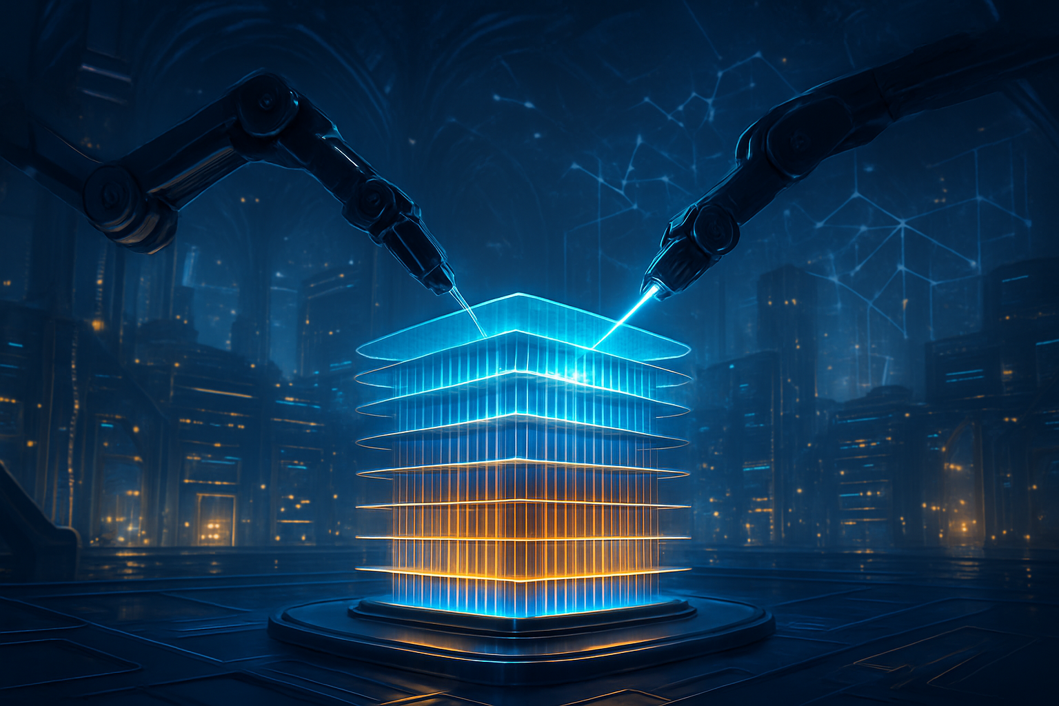
The HBM4 Frontier: A Technical Hurdle of Unprecedented Scale
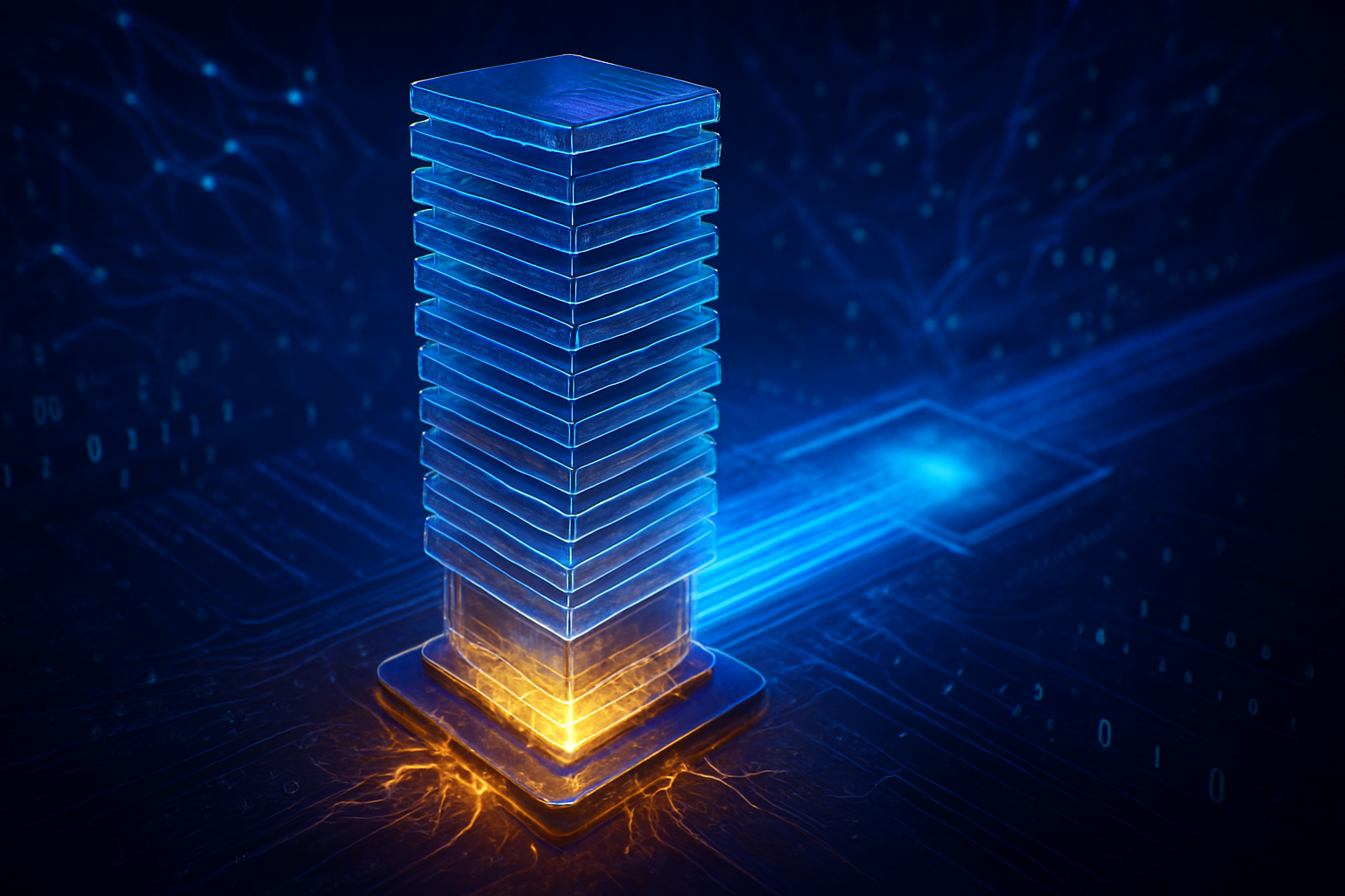
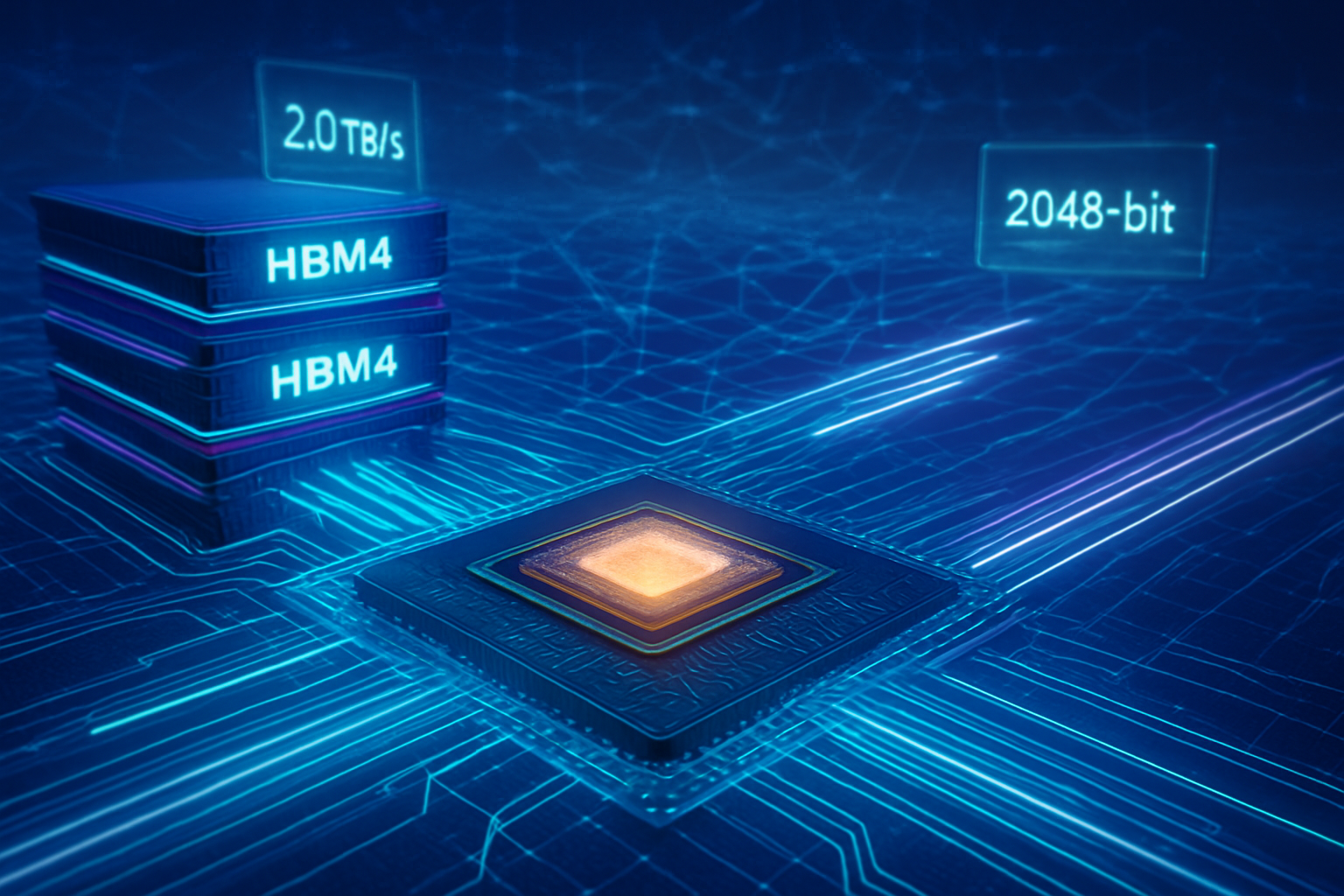
The current shortage is driven largely by the massive technical complexity involved in producing the next generation of memory. The industry is currently transitioning from HBM3e to HBM4, a leap that represents the most significant architectural shift in the history of memory technology. Unlike previous generations, HBM4 doubles the interface width from 1024-bit to a massive 2048-bit bus. This transition requires sophisticated Through-Silicon Via (TSV) techniques and unprecedented precision in stacking.
A primary bottleneck is the "height limit" challenge. To meet JEDEC standards, manufacturers like SK Hynix (KRX: 000660) and Samsung Electronics (KRX: 005930) must stack up to 16 layers of memory within a total height of just 775 micrometers. This requires thinning individual silicon wafers to approximately 30 micrometers—about a third of the thickness of a human hair. Furthermore, the move toward "Hybrid Bonding" (copper-to-copper) for 16-layer stacks has introduced significant yield issues. Samsung, in particular, is pushing this boundary, but initial yields for the most advanced 16-layer HBM4 are reportedly hovering around 10%, a figure that must improve drastically before the 2027 target for market equilibrium can be met.
The industry is also dealing with a "capacity penalty." Because HBM requires more complex manufacturing and has a much larger die size than standard DRAM, producing 1GB of HBM consumes nearly four times the wafer capacity of 1GB of conventional DDR5 memory. This multiplier effect means that even though companies are adding cleanroom space, the actual number of memory bits reaching the market is significantly lower than in previous expansion cycles.
The Triumvirate’s Struggle: Capacity Ramps and Strategic Shifts
The memory market is dominated by a triumvirate of giants: SK Hynix (KRX: 000660), Samsung Electronics (KRX: 005930), and Micron Technology (NASDAQ: MU). Each is racing to bring new capacity online, but the lead times for semiconductor fabrication plants (fabs) are measured in years, not months. SK Hynix is currently the volume leader, utilizing its Mass Reflow Molded Underfill (MR-MUF) technology to maintain higher yields on 12-layer HBM3e, while Micron has announced its 2026 capacity is already entirely sold out to hyperscalers and AI chip designers like NVIDIA (NASDAQ: NVDA) and Advanced Micro Devices (NASDAQ: AMD).
Strategically, these manufacturers are prioritizing their highest-margin products. With HBM margins reportedly exceeding 60%, compared to the 20% typical of commodity consumer DRAM, there is little incentive to prioritize the needs of the PC or smartphone markets. Micron, for instance, recently pivoted its strategy to focus almost exclusively on enterprise-grade AI solutions, reducing its exposure to the volatile consumer retail segment.
The competitive landscape is also being reshaped by the "Yongin Cluster" in South Korea and Micron’s new Boise, Idaho fab. However, these massive infrastructure projects are not expected to reach full-scale output until late 2027 or 2028. In the interim, the leverage remains entirely with the memory suppliers, who are able to command premium prices as AI giants like NVIDIA continue to scale their Blackwell Ultra and upcoming "Rubin" architectures, both of which demand record-breaking amounts of HBM4 memory.
Beyond the Data Center: The Consumer Electronics 'AI Tax'
The wider significance of this shortage is being felt most acutely in the consumer electronics sector, where an "AI Tax" is becoming a reality. According to TrendForce, conventional DRAM contract prices have surged by nearly 60% in the first quarter of 2026. This has directly translated into higher Bill-of-Materials (BOM) costs for original equipment manufacturers (OEMs). Companies like Dell Technologies (NYSE: DELL) and HP Inc. (NYSE: HPQ) have been forced to rethink their product lineups, often eliminating low-margin, budget-friendly laptops in favor of higher-end "AI PCs" that can justify the increased memory costs.
The smartphone market is facing a similar squeeze. High-end devices now require specialized LPDDR5X memory to run on-device AI models, but this specific type of memory is being diverted to secondary roles in servers. As a result, analysts expect the retail price of flagship smartphones to rise by as much as 10% throughout 2026. In some cases, manufacturers are even reverting to older memory standards for mid-range phones to maintain price points, a move that could stunt the adoption of mobile AI features.
Perhaps most surprising is the impact on the automotive industry. Modern electric vehicles and autonomous systems rely heavily on DRAM for infotainment and sensor processing. S&P Global predicts that automotive DRAM prices could double by 2027, as carmakers find themselves outbid by cloud service providers for limited wafer allocations. This is a stark reminder that the AI revolution is not just happening in the cloud; its supply chain ripples are felt in every facet of the digital economy.
Looking Toward 2027: Custom Silicon and the Path to Equilibrium
Looking ahead, the industry is preparing for a transition to HBM4E in late 2027, which promises even higher bandwidth and energy efficiency. However, the path to 2027 is paved with challenges, most notably the shift toward "Custom HBM." In this new model, memory is no longer a commodity but a semi-custom product designed in collaboration with logic foundry giants like TSMC (NYSE: TSM). This allows for better thermal performance and lower latency, but it further complicates the supply chain, as memory must be co-engineered with the AI accelerators it will serve.
Near-term developments will likely focus on stabilizing 16-layer stacking and improving the yields of hybrid bonding. Experts predict that until the yield rates for these advanced processes reach at least 50%, the supply-demand gap will remain wide. We may also see the rise of alternative memory architectures, such as CXL (Compute Express Link), which aims to allow data centers to pool and share memory more efficiently, potentially easing some of the pressure on individual HBM modules.
The ultimate challenge remains the sheer physical limit of wafer production. Until the next generation of fabs in South Korea and the United States comes online in the 2027-2028 timeframe, the industry will have to survive on incremental efficiency gains. Analysts suggest that any unexpected surge in AI demand—such as the sudden commercialization of high-order autonomous agents or a new breakthrough in Large Language Model (LLM) size—could push the equilibrium date even further into the future.
A Structural Shift in the Semiconductor Paradigm
The memory shortage of the mid-2020s is more than just a temporary supply chain hiccup; it represents a fundamental shift in the semiconductor paradigm. The transition from memory as a commodity to memory as a bespoke, high-performance bottleneck for artificial intelligence has permanently changed the market's dynamics. The primary takeaway is that for the next two years, the pace of AI advancement will be dictated as much by the physical limits of silicon stacking as by the ingenuity of software algorithms.
As we move through 2026 and into 2027, the industry must watch for key milestones: the stabilization of HBM4 yields, the progress of greenfield fab constructions, and potential shifts in consumer demand as prices rise. For now, the "Memory Wall" remains the most significant obstacle to the scaling of artificial intelligence.
While the current forecast looks lean for consumers and challenging for hardware OEMs, it signals a period of unprecedented investment and innovation in memory technology. The lessons learned during this 2026-2027 crunch will likely define the architecture of computing for the next decade.
This content is intended for informational purposes only and represents analysis of current AI developments.
TokenRing AI delivers enterprise-grade solutions for multi-agent AI workflow orchestration, AI-powered development tools, and seamless remote collaboration platforms.
For more information, visit https://www.tokenring.ai/.