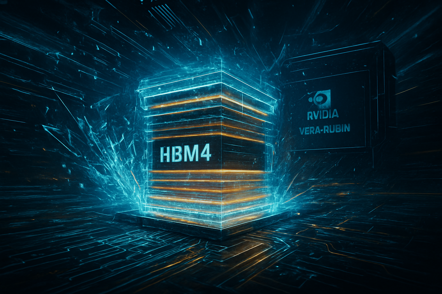
The unveiling of NVIDIA’s (NASDAQ: NVDA) next-generation Rubin architecture has officially ignited the "HBM4 Memory War," a high-stakes competition between the world’s three largest memory manufacturers—SK Hynix (KRX: 000660), Samsung Electronics (KRX: 005930), and Micron Technology (NASDAQ: MU). Unlike previous generations, this is not a mere race for capacity; it is a fundamental redesign of how memory and logic interact to sustain the voracious appetite of trillion-parameter AI models.
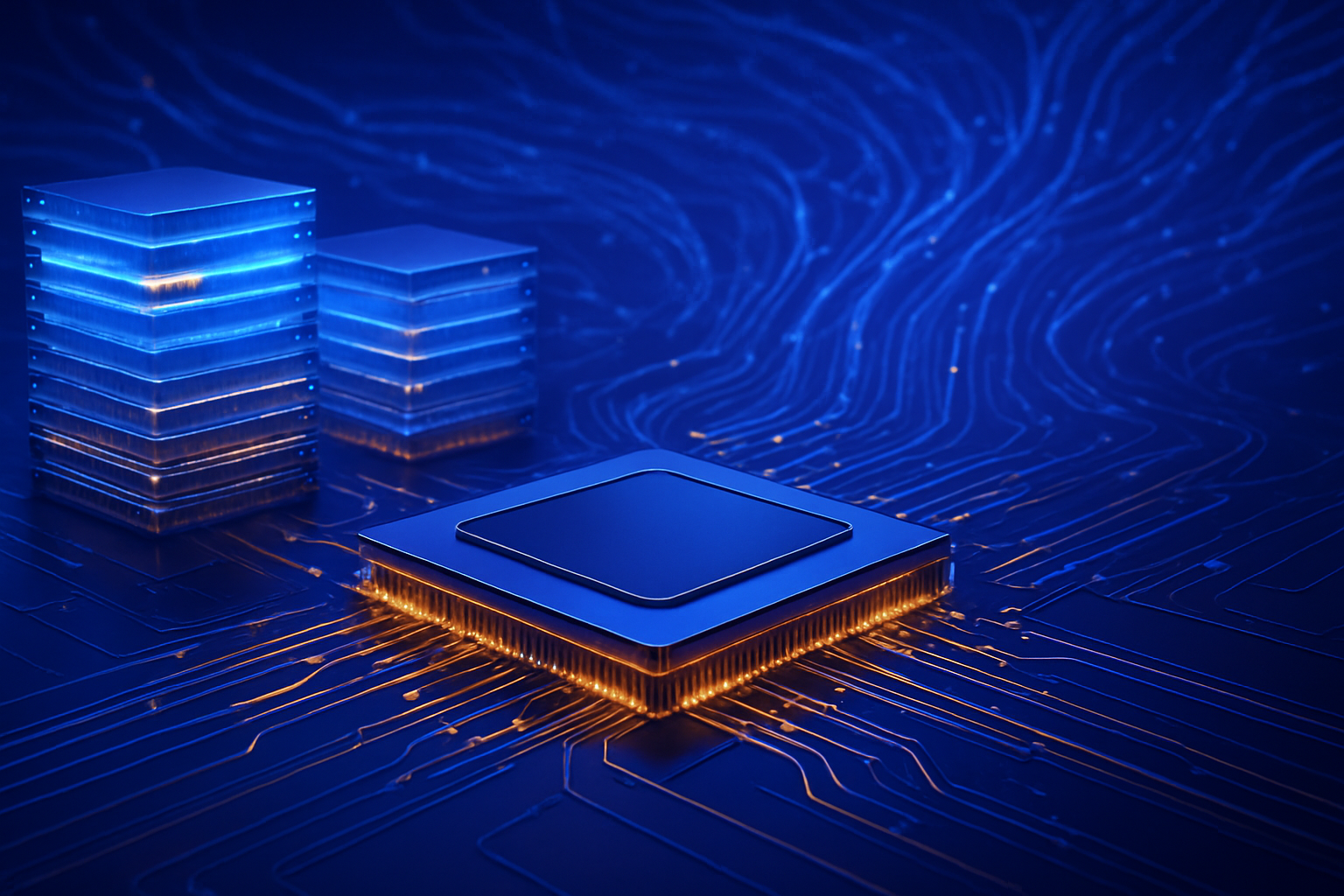
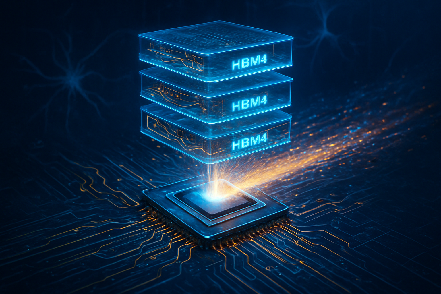
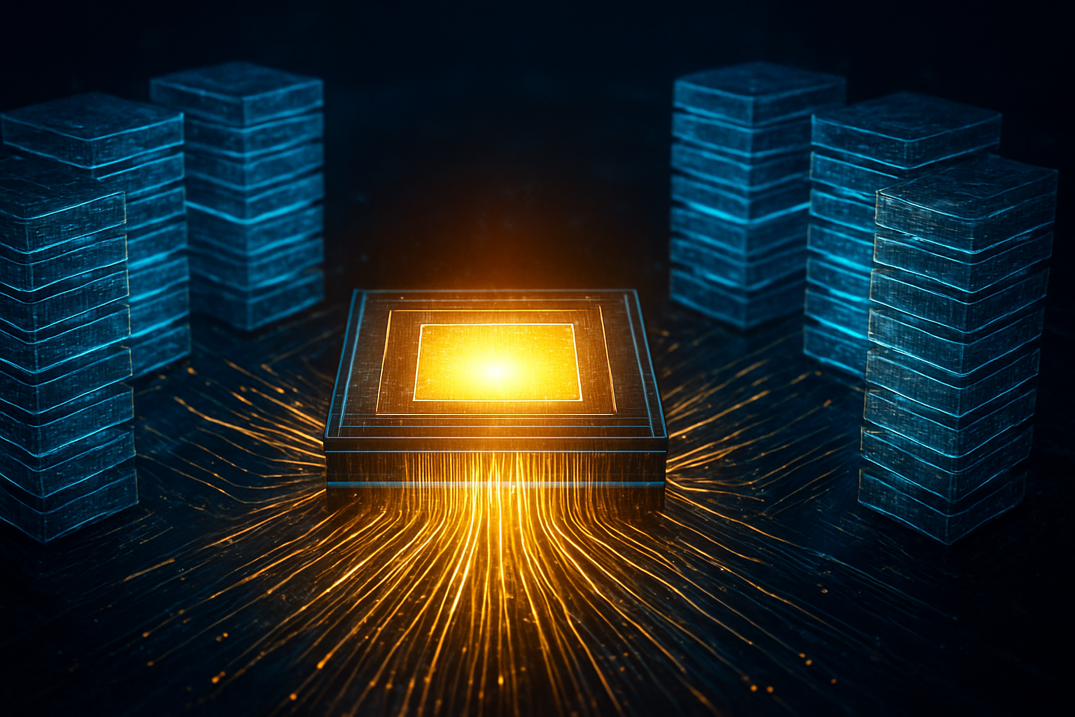
The immediate significance of this development cannot be overstated. With the Rubin R100 GPUs entering mass production this year, the demand for HBM4 (High Bandwidth Memory 4) has created a bottleneck that defines the winners and losers of the AI era. These new GPUs require a staggering 288GB to 384GB of VRAM per package, delivered through ultra-wide interfaces that triple the bandwidth of the previous Blackwell generation. For the first time, memory is no longer a passive storage component but a customized logic-integrated partner, transforming the semiconductor landscape into a battlefield of advanced packaging and proprietary manufacturing techniques.
The 2048-Bit Leap: Engineering the 16-Layer Stack
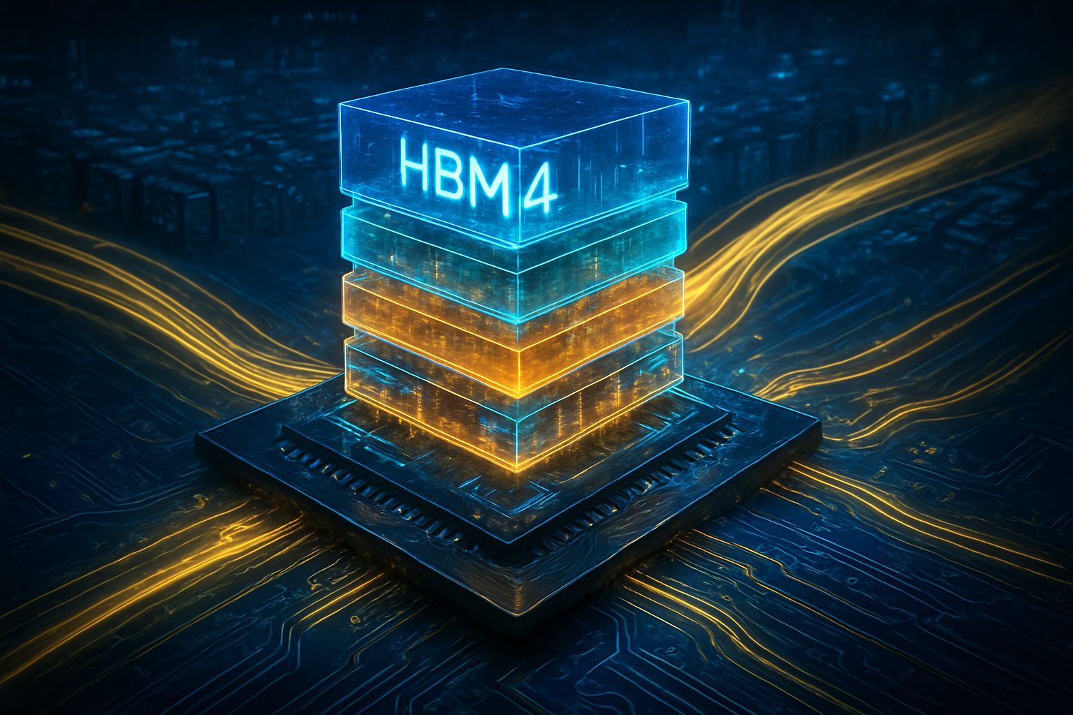
The shift to HBM4 represents the most radical architectural departure in the decade-long history of High Bandwidth Memory. While HBM3e relied on a 1024-bit interface, HBM4 doubles this width to 2048-bit. This "wider pipe" allows for massive data throughput—up to 24 TB/s aggregate bandwidth on a single Rubin GPU—without the astronomical power draw that would come from simply increasing clock speeds. However, doubling the bus width has introduced a "routing nightmare" for engineers, necessitating advanced packaging solutions like TSMC’s (NYSE: TSM) CoWoS-L (Chip-on-Wafer-on-Substrate with Local Interconnect), which can handle the dense interconnects required for these ultra-wide paths.
At the heart of the competition is the 16-layer (16-Hi) stack, which enables capacities of up to 64GB per module. SK Hynix has maintained its early lead by refining its proprietary Advanced Mass Reflow Molded Underfill (MR-MUF) process, managing to thin DRAM wafers to a record 30 micrometers to fit 16 layers within the industry-standard height limits. Samsung, meanwhile, has taken a bolder, higher-risk approach by pioneering Hybrid Bonding for its 16-layer stacks. This "bumpless" stacking method replaces traditional micro-bumps with direct copper-to-copper connections, significantly reducing heat and vertical height, though early reports suggest the company is still struggling with yield rates near 10%.
This generation also introduces the "logic base die," where the bottom layer of the HBM stack is manufactured using a logic process (5nm or 12nm) rather than a traditional DRAM process. This allows the memory stack to handle basic computational tasks, such as data compression and encryption, directly on-die. Experts in the research community view this as a pivotal move toward "processing-in-memory" (PIM), a concept that has long been theorized but is only now becoming a commercial reality to combat the "memory wall" that threatens to stall AI progress.
The Strategic Alliance vs. The Integrated Titan
The competitive landscape for HBM4 has split the industry into two distinct strategic camps. On one side is the "Foundry-Memory Alliance," spearheaded by SK Hynix and Micron. Both companies have partnered with TSMC to manufacture their HBM4 base dies. This "One-Team" approach allows them to leverage TSMC’s world-class 5nm and 12nm logic nodes, ensuring their memory is perfectly tuned for the TSMC-manufactured NVIDIA Rubin GPUs. SK Hynix currently commands roughly 53% of the HBM market, and its proximity to TSMC's packaging ecosystem gives it a formidable defensive moat.
On the other side stands Samsung Electronics, the "Integrated Titan." Leveraging its unique position as the only company in the world that houses a leading-edge foundry, a memory division, and an advanced packaging house under one roof, Samsung is offering a "turnkey" solution. By using its own 4nm node for the HBM4 logic die, Samsung aims to provide higher energy efficiency and a more streamlined supply chain. While yield issues have hampered their initial 16-layer rollout, Samsung’s 1c DRAM process (the 6th generation 10nm node) is theoretically 40% more efficient than its competitors' offerings, positioning them as a major threat for the upcoming "Rubin Ultra" refresh in 2027.
Micron Technology, though currently the smallest of the three by market share, has emerged as a critical "dark horse." At CES 2026, Micron confirmed that its entire HBM4 production capacity for the year is already sold out through advance contracts. This highlights the sheer desperation of hyperscalers like Google (NASDAQ: GOOGL) and Meta (NASDAQ: META), who are bypassing traditional procurement routes to secure memory directly from any reliable source to fuel their internal AI accelerator programs.
Beyond Bandwidth: Memory as the New AI Differentiator
The HBM4 war signals a broader shift in the AI landscape where the processor is no longer the sole arbiter of performance. We are entering an era of "Custom HBM," where the memory stack itself is tailored to specific AI workloads. Because the base die of HBM4 is now a logic chip, AI giants can request custom IP blocks to be integrated directly into the memory they purchase. This allows a company like Amazon (NASDAQ: AMZN) or Microsoft (NASDAQ: MSFT) to optimize memory access patterns for their specific LLMs (Large Language Models), potentially gaining a 15-20% efficiency boost over generic hardware.
This transition mirrors the milestone of the first integrated circuits, where separate components were merged to save space and power. However, the move toward custom memory also raises concerns about industry fragmentation. If memory becomes too specialized for specific GPUs or cloud providers, the "commodity" nature of DRAM could vanish, leading to higher costs and more complex supply chains. Furthermore, the immense power requirements of HBM4—with some Rubin GPU clusters projected to pull over 1,000 watts per package—have made thermal management the primary engineering challenge for the next five years.
The societal implications are equally vast. The ability to run massive models more efficiently means that the next generation of AI—capable of real-time video reasoning and autonomous scientific discovery—will be limited not by the speed of the "brain" (the GPU), but by how fast it can remember and access information (the HBM4). The winner of this memory war will essentially control the "bandwidth of intelligence" for the late 2020s.
The Road to Rubin Ultra and HBM5
Looking toward the near-term future, the HBM4 cycle is expected to be relatively short. NVIDIA has already provided a roadmap for "Rubin Ultra" in 2027, which will utilize an enhanced HBM4e standard. This iteration is expected to push capacities even further, likely reaching 1TB of total VRAM per package by utilizing 20-layer stacks. Achieving this will almost certainly require the industry-wide adoption of hybrid bonding, as traditional micro-bumps will no longer be able to meet the stringent height and thermal requirements of such dense vertical structures.
The long-term challenge remains the transition to 3D integration, where the memory is stacked directly on top of the GPU logic itself, rather than sitting alongside it on an interposer. While HBM4 moves us closer to this reality with its logic base die, true 3D stacking remains a "holy grail" that experts predict will not be fully realized until HBM5 or beyond. Challenges in heat dissipation and manufacturing complexity for such "monolithic" chips are the primary hurdles that researchers at SK Hynix and Samsung are currently racing to solve in their secret R&D labs.
A Decisive Moment in Semiconductor History
The HBM4 memory war is more than a corporate rivalry; it is the defining technological struggle of 2026. As NVIDIA's Rubin architecture begins to populate data centers worldwide, the success of the AI industry hinges on the ability of SK Hynix, Samsung, and Micron to deliver these complex 16-layer stacks at scale. SK Hynix remains the favorite due to its proven MR-MUF process and its tight-knit alliance with TSMC, but Samsung’s aggressive bet on hybrid bonding could flip the script if they can stabilize their yields by the second half of the year.
For the tech industry, the key takeaway is that the era of "generic" hardware is ending. Memory is becoming as intelligent and as customized as the processors it serves. In the coming weeks and months, industry watchers should keep a close eye on the qualification results of Samsung’s 16-layer HBM4 samples; a successful certification from NVIDIA would signal a massive shift in market dynamics and likely trigger a rally in Samsung’s stock. As of January 2026, the lines have been drawn, and the "bandwidth of the future" is currently being forged in the cleanrooms of Suwon, Icheon, and Boise.
This content is intended for informational purposes only and represents analysis of current AI developments.
TokenRing AI delivers enterprise-grade solutions for multi-agent AI workflow orchestration, AI-powered development tools, and seamless remote collaboration platforms.
For more information, visit https://www.tokenring.ai/.