As of January 2026, the artificial intelligence industry has hit a critical juncture where the silicon "brain" is only as fast as its "circulatory system." The race to provide High Bandwidth Memory (HBM)—the essential fuel for the world’s most powerful GPUs—has escalated into a full-scale industrial war. With the transition from HBM3E to the next-generation HBM4 standard now in full swing, the three dominant players, SK Hynix (KRX: 000660), Micron Technology (NASDAQ: MU), and Samsung Electronics (KRX: 005930), are locked in a high-stakes competition to capture the majority of the market for NVIDIA (NASDAQ: NVDA) and its upcoming Rubin architecture.
The significance of this development cannot be overstated: as AI models cross the trillion-parameter threshold, the "memory wall"—the bottleneck caused by the speed difference between processors and memory—has become the primary obstacle to progress. In early 2026, the industry is witnessing an unprecedented supply crunch; as manufacturers retool their lines for HBM4, the price of existing HBM3E has surged by 20%, even as demand for NVIDIA’s Blackwell Ultra chips reaches a fever pitch. The winners of this memory war will not only see record profits but will effectively control the pace of AI evolution for the remainder of the decade.
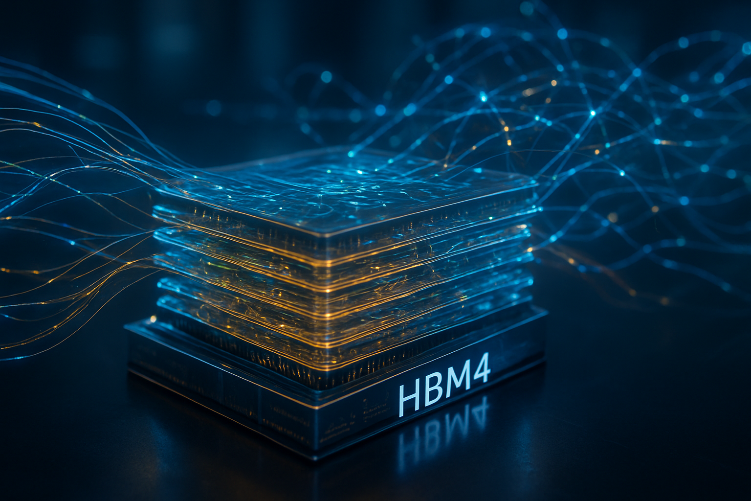
The Technical Leap: HBM4 and the 2048-Bit Revolution
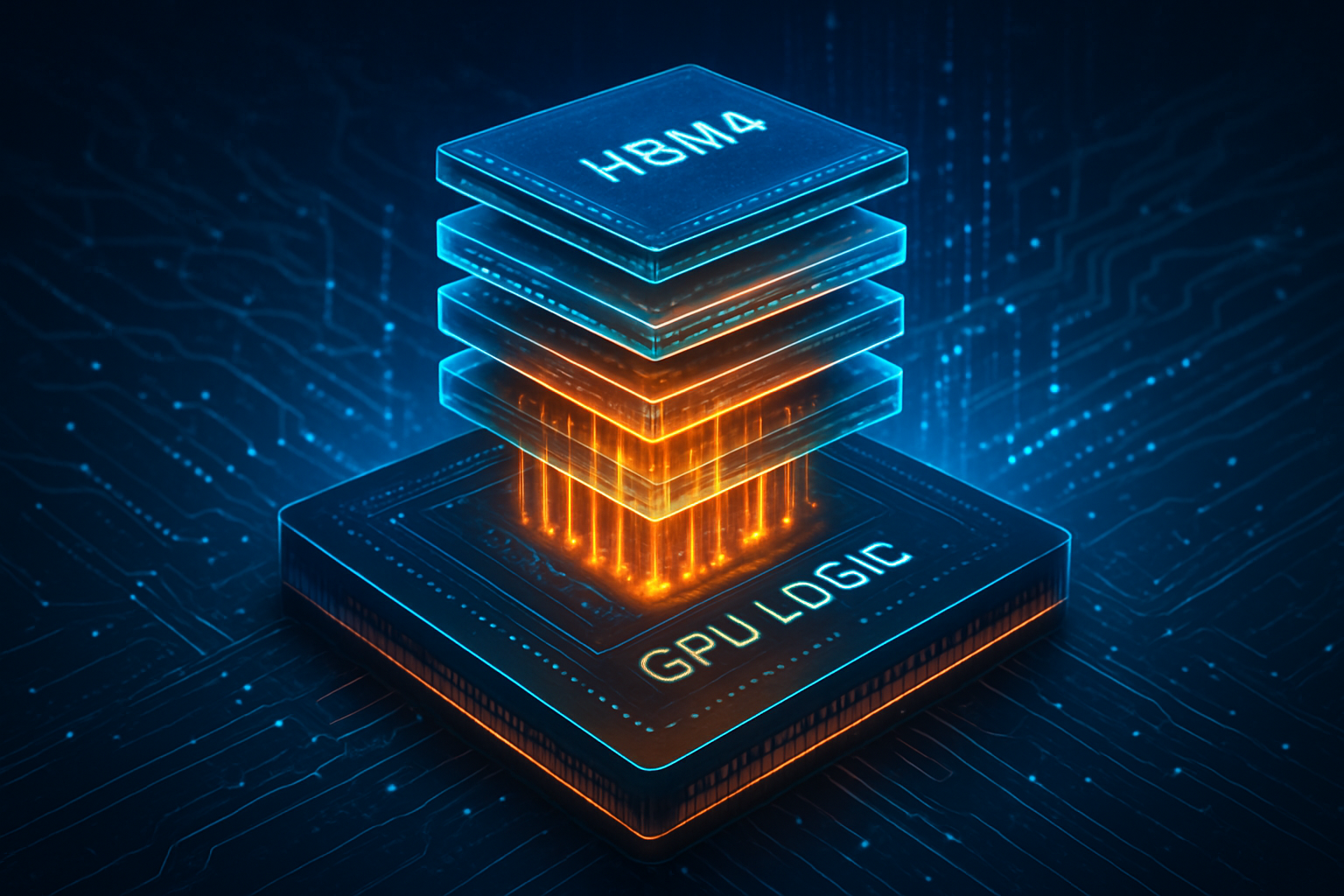
The technical specifications of the new HBM4 standard represent the most significant architectural shift in memory technology in a decade. Unlike the incremental move from HBM3 to HBM3E, HBM4 doubles the interface width from 1024-bit to 2048-bit. This allows for a massive leap in aggregate bandwidth—reaching up to 3.3 TB/s per stack—while operating at lower clock speeds. This reduction in clock speed is critical for managing the immense heat generated by AI superclusters. For the first time, memory is moving toward a "logic-in-memory" approach, where the base die of the HBM stack is manufactured on advanced logic nodes (5nm and 4nm) rather than traditional memory processes.
A major point of contention in the research community is the method of stacking these chips. Samsung is leading the charge with "Hybrid Bonding," a copper-to-copper direct contact method that eliminates the need for traditional micro-bumps between layers. This allows Samsung to fit 16 layers of DRAM into a 775-micrometer package, a feat that requires thinning wafers to a mere 30 micrometers. Meanwhile, SK Hynix has refined its "Advanced MR-MUF" (Mass Reflow Molded Underfill) process to maintain high yields for 12-layer stacks, though it is expected to transition to hybrid bonding for its 20-layer roadmap in 2027. Initial reactions from industry experts suggest that while SK Hynix currently holds the yield advantage, Samsung’s vertical integration—using its own internal foundry—could give it a long-term cost edge.
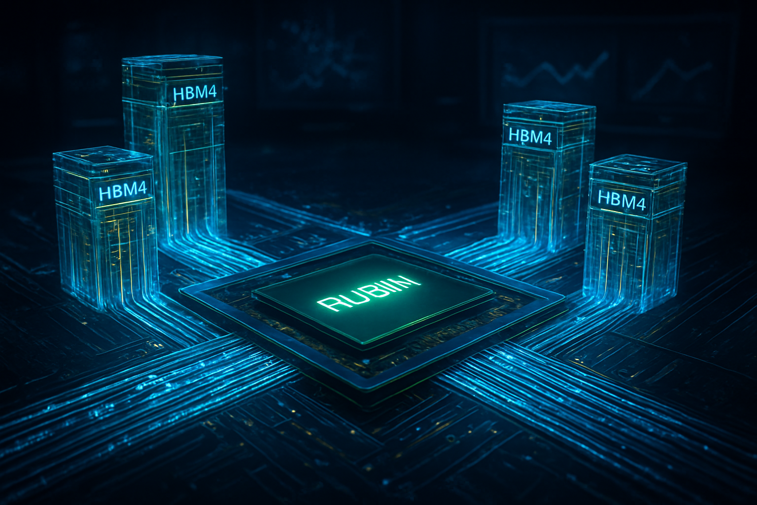
Strategic Positioning: The Battle for the 'Rubin' Crown
The competitive landscape is currently dominated by the "Big Three," but the hierarchy is shifting. SK Hynix remains the incumbent leader, with nearly 60% of the HBM market share and its 2026 capacity already pre-booked by NVIDIA and OpenAI. However, Samsung has staged a dramatic comeback in early 2026. After facing delays in HBM3E certification throughout 2024 and 2025, Samsung recently passed NVIDIA’s rigorous qualification for 12-layer HBM3E and is now the first to announce mass production of HBM4, scheduled for February 2026. This resurgence was bolstered by a landmark $16.5 billion deal with Tesla (NASDAQ: TSLA) to provide HBM4 for their next-generation Dojo supercomputer chips.
Micron, though holding a smaller market share (projected at 15-20% for 2026), has carved out a niche as the "efficiency king." By focusing on power-per-watt leadership, Micron has become a secondary but vital supplier for NVIDIA’s Blackwell B200 and GB300 platforms. The strategic advantage for NVIDIA is clear: by fostering a three-way war, they can prevent any single supplier from gaining too much pricing power. For the AI labs, this competition is a double-edged sword. While it drives innovation, the rapid transition to HBM4 has created a "supply air gap," where HBM3E availability is tightening just as the industry needs it most for mid-tier deployments.
The Wider Significance: AI Sovereignty and the Energy Crisis
This memory war fits into a broader global trend of "AI Sovereignty." Nations and corporations are realizing that the ability to train massive models is tethered to the physical supply of HBM. The shift to HBM4 is not just about speed; it is about the survival of the AI industry's growth trajectory. Without the 2048-bit interface and the power efficiencies of HBM4, the electricity requirements for the next generation of data centers would become unsustainable. We are moving from an era where "compute is king" to one where "memory is the limit."
Comparisons are already being made to the 2021 semiconductor shortage, but with higher stakes. The potential concern is the concentration of manufacturing in East Asia, specifically South Korea. While the U.S. CHIPS Act has helped Micron expand its domestic footprint, the core of the HBM4 revolution remains centered in the Pyeongtaek and Cheongju clusters. Any geopolitical instability could immediately halt the development of trillion-parameter models globally. Furthermore, the 20% price hike in HBM3E contracts seen this month suggests that the cost of "AI fuel" will remain a significant barrier to entry for smaller startups, potentially centralizing AI power among the "Magnificent Seven" tech giants.
Future Outlook: Toward 1TB Memory Stacks and CXL
Looking ahead to late 2026 and 2027, the industry is already preparing for "HBM4E." Experts predict that by 2027, we will see the first 1-terabyte (1TB) memory configurations on a single GPU package, utilizing 16-Hi or even 20-Hi stacks. Beyond just stacking more layers, the next frontier is CXL (Compute Express Link), which will allow for memory pooling across entire racks of servers, effectively breaking the physical boundaries of a single GPU.
The immediate challenge for 2026 will be the transition to 16-layer HBM4. The physics of thinning silicon to 30 micrometers without introducing defects is the "moonshot" of the semiconductor world. If Samsung or SK Hynix can master 16-layer yields by the end of this year, it will pave the way for NVIDIA's "Rubin Ultra" platform, which is expected to target the first 100-trillion parameter models. Analysts at TokenRing AI suggest that the successful integration of TSMC (NYSE: TSM) logic dies into HBM4 stacks—a partnership currently being pursued by both SK Hynix and Micron—will be the deciding factor in who wins the 2027 cycle.
Conclusion: The New Foundation of Intelligence
The HBM3E and HBM4 memory war is more than a corporate rivalry; it is the construction of the foundation for the next era of human intelligence. As of January 2026, the transition to HBM4 marks the moment AI hardware moved away from traditional PC-derived architectures toward something entirely new and specialized. The key takeaway is that while NVIDIA designs the brains, the trio of SK Hynix, Samsung, and Micron are providing the vital energy and data throughput that makes those brains functional.
The significance of this development in AI history will likely be viewed as the moment the "Memory Wall" was finally breached, enabling the move from generative chatbots to truly autonomous, trillion-parameter agents. In the coming weeks, all eyes will be on Samsung’s Pyeongtaek campus as mass production of HBM4 begins. If yields hold steady, the AI industry may finally have the fuel it needs to reach the next frontier.
This content is intended for informational purposes only and represents analysis of current AI developments.
TokenRing AI delivers enterprise-grade solutions for multi-agent AI workflow orchestration, AI-powered development tools, and seamless remote collaboration platforms.
For more information, visit https://www.tokenring.ai/.