Tag: SMIC

  • Silicon Sovereignty: How Huawei and SMIC are Neutralizing US Export Controls in 2026

    Silicon Sovereignty: How Huawei and SMIC are Neutralizing US Export Controls in 2026

    As of January 2026, the technological rift between Washington and Beijing has evolved from a series of trade skirmishes into a permanent state of managed decoupling. The "Chip War" has entered a high-stakes phase where legislative restrictions are being met with aggressive domestic innovation. The recent passage of the AI Overwatch Act in the United States and the introduction of a "national security fee" on high-end silicon exports have signaled a new era of protectionism. In response, China has pivoted toward a "Parallel Purchase" policy, mandating that for every advanced Western chip imported, a domestic equivalent must be deployed, fundamentally altering the global supply chain for artificial intelligence.

    This strategic standoff reached a boiling point in mid-January 2026 when the U.S. government authorized the export of NVIDIA (NASDAQ: NVDA) H200 AI chips to China—but only under a restrictive framework. These chips now carry a 25% tariff and require rigorous certification that they will not be used for state surveillance or military applications. However, the significance of this move is being eclipsed by the rapid advancement of China’s own semiconductor ecosystem. Led by Huawei and Semiconductor Manufacturing International Corp (HKG: 0981) (SMIC), the Chinese domestic market is no longer just surviving under sanctions; it is beginning to thrive by building a self-sufficient "sovereign AI" stack that circumvents Western lithography and memory bottlenecks.

    The Technical Leap: 5nm Mass Production and In-House HBM

    The most striking technical development of early 2026 is SMIC’s successful high-volume production of the N+3 node, a 5nm-class process. Despite being denied access to ASML (NASDAQ: ASML) Extreme Ultraviolet (EUV) lithography machines, SMIC has managed to stretch Deep Ultraviolet (DUV) multi-patterning to its theoretical limits. While industry analysts estimate SMIC’s yields at a modest 30% to 40%—far below the 80% plus achieved by TSMC—the Chinese government has moved to subsidize these inefficiencies, viewing the production of 5nm logic as a matter of national security rather than short-term profit. This capability powers the new Kirin 9030 chipset, which is currently driving Huawei’s latest flagship smartphone rollout across Asia.

    Parallel to the manufacturing gains is Huawei’s breakthrough in the AI accelerator market with the Ascend 950 series. Released in Q1 2026, the Ascend 950PR and 950DT are the first Chinese chips to feature integrated in-house High Bandwidth Memory (HBM). By developing its own HBM solutions, Huawei has effectively bypassed the global shortage and the US-led restrictions on memory exports from leaders like SK Hynix and Samsung. Although the Ascend 950 still trails NVIDIA’s Blackwell architecture in raw FLOPS (floating-point operations per second), its integration with Huawei’s CANN (Compute Architecture for Neural Networks) software stack provides a "mature" alternative that is increasingly attractive to Chinese hyperscalers who are weary of the unpredictable nature of US export licenses.

    Market Disruption: The Decline of the Western Hegemony in China

    The impact on major tech players is profound. NVIDIA, which once commanded over 90% of the Chinese AI chip market, has seen its share plummet to roughly 50% as of January 2026. The combination of the 25% "national security" tariff and Beijing’s "buy local" mandates has made American silicon prohibitively expensive. Furthermore, the AI Overwatch Act has introduced a 30-day Congressional review period for advanced chip sales, creating a level of bureaucratic friction that is pushing Chinese firms like Alibaba (NYSE: BABA), Tencent (HKG: 0700), and ByteDance toward domestic alternatives.

    This shift is not limited to chip designers. Equipment giant ASML has warned investors that its 2026 revenue from China will decline significantly due to a new Chinese "50% Mandate." This regulation requires all domestic fabrication plants (fabs) to source at least half of their equipment from local vendors. Consequently, Chinese equipment makers like Naura Technology Group (SHE: 002371) and Shanghai Micro Electronics Equipment (SMEE) are seeing record order backlogs. Meanwhile, emerging AI chipmakers such as Cambricon have reported a 14-fold increase in revenue over the last fiscal year, positioning themselves as critical suppliers for the massive Chinese data center build-outs that power local LLMs (Large Language Models).

    A Landscape Divided: The Rise of Parallel AI Ecosystems

    The broader significance of the current US-China chip war lies in the fragmentation of the global AI landscape. We are witnessing the birth of two distinct technological ecosystems that operate on different hardware, different software kernels, and different regulatory philosophies. The "lithography gap" that once seemed insurmountable is closing faster than Western experts predicted. The 2025 milestone of a domestic EUV lithography prototype in Shenzhen—developed by a coalition of state researchers and former international engineers—has proven that China is on a path to match Western hardware capabilities within the decade.

    However, this divergence raises significant concerns regarding global AI safety and standardization. With China moving entirely off Western Electronic Design Automation (EDA) tools and adopting domestic software from companies like Empyrean, the ability for international bodies to monitor AI development or implement global safety protocols is diminishing. The world is moving away from the "global village" of hardware and toward "silicon islands," where the security of the supply chain is prioritized over the efficiency of the global market. This mirrors the early 20th-century arms race, but instead of dreadnoughts and steel, the currency of power is transistors and HBM bandwidth.

    The Horizon: 3nm R&D and Domestic EUV Scale

    Looking ahead to the remainder of 2026 and 2027, the focus will shift to Gate-All-Around (GAA) architecture. Reports indicate that Huawei has already begun "taping out" its first 3nm designs using GAA, with a target for mass production in late 2027. If successful, this would represent a jump over several technical hurdles that usually take years to clear. The industry is also closely watching the scale-up of China's domestic EUV program. While the current prototype is a laboratory success, the transition to a factory-ready machine will be the final test of China’s semiconductor independence.

    In the near term, we expect to see an "AI hardware saturation" in China, where the volume of domestic chips offsets their slightly lower performance compared to Western equivalents. Developers will likely focus on optimizing software for these specific domestic architectures, potentially creating a situation where Chinese AI models become more "hardware-efficient" out of necessity. The challenge remains the yield rate; for China to truly compete on the global stage, SMIC must move its 5nm yields from the 30% range toward the 70% range to make the technology economically sustainable without massive state infusions.

    Final Assessment: The Permanent Silicon Wall

    The events of early 2026 confirm that the semiconductor supply chain has been irrevocably altered. The US-China chip war is no longer a temporary disruption but a fundamental feature of the 21st-century geopolitical landscape. Huawei and SMIC have demonstrated remarkable resilience, proving that targeted sanctions can act as a catalyst for domestic innovation rather than just a barrier. The "Silicon Wall" is now a reality, with the West and East building their futures on increasingly incompatible foundations.

    As we move forward, the metric for success will not just be the number of transistors on a chip, but the stability and autonomy of the entire stack—from the light sources in lithography machines to the high-bandwidth memory in AI accelerators. Investors and tech leaders should watch for the results of the first "1-to-1" purchase audits in China and the progress of the US AI Overwatch committee. The battle for silicon sovereignty has just begun, and its outcome will dictate the trajectory of artificial intelligence for the next generation.


    This content is intended for informational purposes only and represents analysis of current AI developments.

    TokenRing AI delivers enterprise-grade solutions for multi-agent AI workflow orchestration, AI-powered development tools, and seamless remote collaboration platforms.
    For more information, visit https://www.tokenring.ai/.

  • China’s “Sovereign” Silicon: Breakthrough in Domestic High-Energy Ion Implantation

    China’s “Sovereign” Silicon: Breakthrough in Domestic High-Energy Ion Implantation

    In a milestone that signals a definitive shift in the global semiconductor balance of power, the China Institute of Atomic Energy (CIAE) announced on January 12, 2026, the successful beam extraction and performance validation of the POWER-750H, China’s first domestically developed tandem-type high-energy hydrogen ion implanter. This development represents the completion of the "final piece" in China’s domestic chipmaking puzzle, closing the technology gap in one of the few remaining "bottleneck" areas where the country was previously 100% dependent on imports from US and Japanese vendors.

    The immediate significance of the POWER-750H cannot be overstated. High-energy ion implantation is a critical process for manufacturing the specialized power semiconductors and image sensors that drive modern AI data centers and electric vehicles. By mastering this technology amidst intensifying trade restrictions, China has effectively neutralized a key lever of Western export controls, securing the foundational equipment needed to scale its internal AI infrastructure and power electronics industry without fear of further technological decapitation.

    Technical Mastery: The Power of Tandem Acceleration

    The POWER-750H is not merely an incremental improvement but a fundamental leap in domestic precision engineering. Unlike standard medium-current implanters, high-energy systems must accelerate ions to mega-electron volt (MeV) levels to penetrate deep into silicon wafers. The "750" in its designation refers to its 750kV high-voltage terminal, which, through tandem acceleration, allows it to generate ion beams with effective energies exceeding 1.5 MeV. This technical capability is essential for "deep junction" doping—a process required to create the robust transistors found in high-voltage power management ICs (PMICs) and high-density memory.

    Technically, the POWER-750H differs from previous Chinese attempts by utilizing a tandem accelerator architecture, which uses a single high-voltage terminal to accelerate ions twice, significantly increasing energy efficiency and beam stability within a smaller footprint. This approach mirrors the advanced systems produced by industry leaders like Axcelis Technologies (NASDAQ: ACLS), yet it has been optimized for the specific "profile engineering" required for wide-bandgap semiconductors like Silicon Carbide (SiC) and Gallium Nitride (GaN). Initial reactions from the domestic research community suggest that the POWER-750H achieves a beam purity and dose uniformity that rivals the venerable Purion series from Axcelis, marking a transition from laboratory prototype to industrial-grade tool.

    Market Seismic Shifts: SMIC, Wanye, and the Retreat of the Giants

    The commercialization of these tools is already reshaping the financial landscape of the semiconductor industry. SMIC (HKG: 0981), China’s largest foundry, has reportedly recalibrated its 2026 capital expenditure (CAPEX) strategy, allocating over 70% of its equipment budget to domestic vendors. This "national team" pivot has provided a massive tailwind for Wanye Enterprises (SHA: 600641), whose subsidiary, Kingsemi, has moved into mass deployment of high-energy models. Market analysts predict that Wanye will capture nearly 40% of the domestic ion implanter market share by the end of 2026, a space that was once an uncontested monopoly for Western firms.

    Conversely, the impact on US equipment giants has been severe. Applied Materials (NASDAQ: AMAT), which historically derived a significant portion of its revenue from the Chinese market, has seen its China-based sales guidance drop from 40% to approximately 25% for the 2026 fiscal year. Even more dramatic was the late-2025 defensive merger between Axcelis and Veeco Instruments (NASDAQ: VECO), a move widely interpreted as an attempt to diversify away from a pure-play ion implantation focus as Chinese domestic alternatives began to saturate the power semiconductor market. The loss of the Chinese "legacy node" and power-chip markets has forced these companies to pivot aggressively toward advanced packaging and High Bandwidth Memory (HBM) tools in the US and South Korea to sustain growth.

    The AI Connection: Powering the Factories of the Future

    Beyond the fabrication of logic chips, the significance of high-energy ion implantation lies in its role in the "AI infrastructure supercycle." Modern AI data centers, which are projected to consume massive amounts of power by the end of 2026, rely on high-efficiency power management systems to operate. Domestic high-energy implanters allow China to produce the specialized MOSFETs and IGBTs needed for these data centers internally. This ensures that China's push for "AI Sovereignty"—the ability to train and run massive large language models on an entirely domestic hardware stack—remains on track.

    This milestone is a pivotal moment in the broader trend of global "de-globalization" in tech. Just as the US has sought to restrict China’s access to 3nm and 5nm lithography, China has responded by achieving self-sufficiency in the tools required for the "power backbone" of AI. This mirrors previous breakthroughs in etching and thin-film deposition, signaling that the era of using semiconductor equipment as a geopolitical weapon may be reaching a point of diminishing returns. The primary concern among international observers is that a fully decoupled supply chain could lead to a divergence in technical standards, potentially slowing the global pace of AI innovation through fragmentation.

    The Horizon: From 28nm to the Sub-7nm Frontier

    Looking ahead, the near-term focus for Chinese equipment manufacturers is the qualification of high-energy tools for the 14nm and 7nm nodes. While the POWER-750H is currently optimized for power chips and 28nm logic, engineers at CETC and Kingsemi are already working on "ultra-high-energy" variants capable of the 5 MeV+ levels required for advanced CMOS image sensors and 3D NAND flash memory. These future iterations are expected to incorporate more advanced automation and AI-driven process control to further increase wafer throughput.

    The most anticipated development on the horizon is the integration of these domestic tools into the production lines for Huawei’s next-generation Ascend 910D AI accelerators. Experts predict that by late 2026, China will demonstrate a "fully domestic" 7nm production line that utilizes zero US-origin equipment. The challenge remains in achieving the extreme ultraviolet (EUV) lithography parity required for sub-5nm chips, but with the ion implantation hurdle cleared, the path toward total semiconductor independence is more visible than ever.

    A New Era of Semiconductor Sovereignty

    The announcement of the POWER-750H is more than a technical victory; it is a geopolitical statement. It marks the moment when China transitioned from being a consumer of semiconductor technology to a self-sustaining architect of its own silicon future. The key takeaway for the tech industry is that the window for using specialized equipment exports to stifle Chinese semiconductor growth is rapidly closing.

    In the coming months, the industry will be watching for the first production data from SMIC’s domestic-only lines and the potential for these Chinese tools to begin appearing in secondary markets in Southeast Asia and Europe. As 2026 unfolds, the successful deployment of the POWER-750H will likely be remembered as the event that solidified the "Two-Track" global semiconductor ecosystem, forever changing the competitive dynamics of the AI and chipmaking industries.


    This content is intended for informational purposes only and represents analysis of current AI and semiconductor developments.

    TokenRing AI delivers enterprise-grade solutions for multi-agent AI workflow orchestration, AI-powered development tools, and seamless remote collaboration platforms.
    For more information, visit https://www.tokenring.ai/.

  • China Enforces 50% Domestic Equipment Mandate to Shield Semiconductor Industry from US Restrictions

    China Enforces 50% Domestic Equipment Mandate to Shield Semiconductor Industry from US Restrictions

    In a decisive move to solidify its technological sovereignty, Beijing has officially enforced a mandate requiring domestic chipmakers to source at least 50% of their manufacturing equipment from local suppliers. This strategic policy, a cornerstone of the evolved 'Made in China 2025' initiative, marks a transition from defensive posturing against Western sanctions to a proactive restructuring of the global semiconductor supply chain. By mandating a domestic floor for procurement, China is effectively insulating its foundational 14nm and 28nm production lines from the reach of U.S. export controls.

    The enforcement of this mandate comes at a critical juncture in early 2026, as the "Whole-Nation System" (Juguo Tizhi) begins to yield tangible results in narrowing the technical gaps previously dominated by Western firms. The policy is not merely a symbolic gesture; it is a strict regulatory requirement for any new fabrication facility or capacity expansion. As domestic giants like NAURA Technology Group (SZSE: 002371) and SMIC (Semiconductor Manufacturing International Corporation) (HKG: 0981) see their order books swell, the global semiconductor landscape is witnessing a structural decoupling that could redefine the industry for the next decade.

    Technical Milestones: Achieving Self-Sufficiency in Mature Nodes

    The 50% mandate is anchored in the rapid maturation of Chinese semiconductor equipment. While the global industry has historically relied on a handful of players for critical tools, Chinese firms have made significant strides in etching, thin-film deposition, and cleaning processes. NAURA Technology Group (SZSE: 002371) has emerged as a powerhouse, with its oxidation and diffusion furnaces now accounting for over 60% of the equipment on SMIC's 28nm production lines. This level of penetration demonstrates that for mature nodes—the workhorses of the automotive, IoT, and industrial sectors—China has effectively achieved "controllable" status.

    Beyond mature nodes, the technical narrative in early 2026 is dominated by "lithography bypass" strategies. Since access to advanced Extreme Ultraviolet (EUV) tools remains restricted, Chinese engineers have pivoted to Self-Aligned Quadruple Patterning (SAQP). This complex multi-patterning technique has allowed SMIC to push its 7nm yields to approximately 70%, a significant improvement from previous years. Furthermore, the industry is moving toward "Virtual 3nm" performance by utilizing advanced packaging and chiplet architectures. By "stitching" together multiple 7nm chiplets using the newly established Advanced Chiplet Cloud (ACC) 1.0 standard, China is producing high-performance processors that rival the compute power of single-die chips from the West.

    Initial reactions from the global AI research community suggest that while these "Virtual 3nm" chips may have slightly higher power consumption and larger physical footprints, their raw performance is more than sufficient for large-scale AI training. Experts note that this shift toward architectural innovation over pure transistor shrinking is a direct result of the supply chain pressures. While the U.S. continues to focus on denying access to the smallest transistors, China is proving that system-level integration can bridge much of the gap.

    Market Impact: National Champions Rise as Western Giants Face Headwinds

    The enforcement of the 50% mandate has triggered a massive realignment of market shares within China. NAURA Technology Group reported record profits for the 2025 fiscal year, even surpassing the foundry leader SMIC in total earnings growth. Other domestic players, such as Advanced Micro-Fabrication Equipment Inc. (AMEC) (SHA: 688012) and Piotech Inc. (SHA: 688072), are seeing their market caps surge as they replace tools formerly supplied by Applied Materials (NASDAQ: AMAT) and Lam Research (NASDAQ: LRCX). This domestic preference is creating a "virtuous cycle" where increased revenue for local firms leads to higher R&D spending, further accelerating the replacement of Western technology.

    Conversely, the mandatory 50% floor represents a significant challenge for Western equipment manufacturers who have historically relied on the Chinese market for a large portion of their revenue. Companies like ASML (NASDAQ: ASML) and Applied Materials are finding their "addressable market" in China shrinking to the most advanced nodes where domestic alternatives do not yet exist. In response to these shifting dynamics, the U.S. Department of Commerce has adopted a more transactional approach, recently allowing limited sales of Nvidia (NASDAQ: NVDA) H200 AI chips to China, provided the U.S. government receives a 25% revenue cut.

    However, even this "pay-to-play" model is facing resistance. In early 2026, Chinese customs reportedly blocked several shipments of high-end Western AI silicon, signaling that Beijing is increasingly confident in its domestic alternatives. This suggests a strategic shift: China is no longer just looking for a "workaround" to U.S. sanctions; it is actively looking to phase out Western dependency entirely. For startups and smaller AI labs in China, the 50% mandate ensures a steady supply of domestic hardware, reducing the "sanction risk" that has plagued the industry for the last three years.

    The 'Whole-Nation System' and the Broader AI Landscape

    The success of the 50% mandate is deeply intertwined with China's "New-Type Whole-Nation System." This centralized economic strategy mobilizes state capital, academic research, and private enterprise toward a singular goal: total semiconductor independence. The deployment of Big Fund III, which was registered with a staggering $49 billion (344 billion RMB) in 2024, has been instrumental in this effort. Unlike previous iterations of the fund that focused on broad infrastructure, Big Fund III is highly targeted, focusing on specific "choke point" technologies such as High Bandwidth Memory (HBM) and 3D hybrid bonding.

    This development fits into a broader global trend of "tech-nationalism," where semiconductor manufacturing is increasingly viewed as a matter of national security rather than just commercial competition. China's move mirrors similar efforts in the U.S. via the CHIPS Act, but with a more aggressive, state-mandated procurement requirement. The impact is a bifurcated global AI landscape, where the East and West operate on different technical standards and hardware ecosystems. The introduction of the ACC 1.0 interconnect protocol is a clear signal that China intends to set its own standards, potentially creating a "Great Firewall" of hardware that is incompatible with Western systems.

    There are, however, significant concerns regarding the long-term efficiency of this approach. Critics argue that forcing the use of domestic equipment could lead to higher production costs and slower innovation compared to a global, open market. Comparisons are being made to historical "import substitution" models that have had mixed results in other industries. Yet, proponents of the "Whole-Nation System" point to the rapid progress in 14nm and 28nm yields as proof that the model is working, effectively filling the technical gaps left by restricted Western manufacturers.

    Future Horizons: From 28nm to EUV Breakthroughs

    Looking ahead to the remainder of 2026 and 2027, the industry is closely watching for the next major technical milestone: a domestic Extreme Ultraviolet (EUV) lithography system. Reports have emerged of an EUV prototype undergoing testing in Shenzhen, utilizing Laser-Induced Discharge Plasma (LDP) technology. This approach is claimed to be more power-efficient than the methods used by current market leaders. If these trials are successful, mass production could begin as early as late 2027, which would represent the final "boss level" in China's quest for chip self-sufficiency.

    Near-term developments will likely focus on the expansion of "chiplet-based" AI accelerators. As the 50% mandate ensures a stable supply of mature-node components, Chinese AI companies are expected to launch a new wave of enterprise-grade AI servers that utilize multi-chip modules to achieve high compute density. These products will likely target domestic data centers and "Global South" markets, where Western export restrictions are less influential. The challenge remains in the software ecosystem, where Western frameworks still dominate, but the "ACC 1.0" standard is the first step in creating a competitive Chinese software-hardware stack.

    Summary and Outlook

    China’s enforcement of the 50% domestic equipment mandate is a watershed moment in the history of the semiconductor industry. It signals that the era of globalized chip manufacturing is giving way to a more fragmented, nationalistic model. For China, the policy is a necessary shield against external volatility; for the rest of the world, it is a clear indication that the "middle kingdom" is prepared to build its own future, one transistor—and one domestic tool—at a time.

    As we move through 2026, the key metrics to watch will be the domestic substitution rate for lithography and the commercial success of "Virtual 3nm" chiplet designs. If China can maintain its current trajectory, the 50% mandate will be remembered as the policy that transformed a defensive industry into a global powerhouse. For now, the message from Beijing is clear: the path to technological self-reliance is non-negotiable, and the tools of the future will be made at home.


    This content is intended for informational purposes only and represents analysis of current AI developments.

    TokenRing AI delivers enterprise-grade solutions for multi-agent AI workflow orchestration, AI-powered development tools, and seamless remote collaboration platforms.
    For more information, visit https://www.tokenring.ai/.

  • The Silicon Curtain Descends: 2026 Trade Policies and the Struggle for Chip Sovereignty

    The Silicon Curtain Descends: 2026 Trade Policies and the Struggle for Chip Sovereignty

    As of January 7, 2026, the global semiconductor industry has entered a precarious new era defined by a "Silicon Curtain" that is bifurcating the world’s most critical supply chain. Following a landmark determination by the Office of the U.S. Trade Representative (USTR) on December 23, 2025, a new phase of Section 301 tariffs has been implemented, specifically targeting Chinese-made semiconductors. While the initial tariff rate is set at 0% to avoid immediate inflationary shocks to the automotive and consumer electronics sectors, this "grace period" is a calculated tactical move, with a massive, yet-to-be-specified rate hike already scheduled for June 23, 2027.

    This policy shift, combined with a tightening trilateral equipment blockade between the U.S., Japan, and the Netherlands, has forced a dramatic realignment of global chip manufacturing. While Washington aims to incentivize a migration of the supply chain away from Chinese foundries, Beijing has responded by doubling down on its "whole-of-nation" push for self-sufficiency. However, as the new year begins, the technical reality on the ground for Chinese champions like Semiconductor Manufacturing International Corp. (SMIC) (HKG: 0981) and Hua Hong Semiconductor (HKG: 1347) remains one of significant yield challenges and operational friction.

    The technical backbone of the current trade friction lies in the sophisticated layering of fiscal and export controls. The U.S. government’s decision to start the new Section 301 tariffs at 0% serves as a "ticking clock" for Western companies to find alternative sourcing for legacy chips—the 28nm to 90nm components that power everything from washing machines to F-150 trucks. By 2027, these duties will be added to the existing 50% tariffs already in place, effectively pricing Chinese-made general-purpose chips out of the American market. This is not merely a tax; it is a forced migration of the global electronics ecosystem.

    Simultaneously, the "Trilateral Blockade" involving the U.S., Japan, and the Netherlands has moved beyond restricting the sale of new machines to targeting the maintenance of existing ones. As of April 2025, ASML (NASDAQ: ASML) has been required to seek direct licenses from the Dutch government to service immersion Deep Ultraviolet (DUV) lithography systems already installed in China. Japan has followed suit, with Tokyo Electron (TYO: 8035) and Nikon (TYO: 7731) expanding their export controls to include over 23 types of advanced equipment and, crucially, the spare parts and software updates required to keep them running. This "service choke" is causing an estimated 15% to 20% annual attrition rate in the precision of Chinese fab lines, as machines fall out of calibration without factory-authorized support.

    The immediate beneficiaries of this geopolitical tension are non-Chinese foundries capable of producing legacy and mid-range nodes. Taiwan Semiconductor Manufacturing Company (TSMC) (NYSE: TSM) and Intel (NASDAQ: INTC) are seeing a surge in "China-plus-one" orders as global OEMs seek to de-risk their 2027 exposure. Conversely, Chinese firms are facing a brutal financial squeeze. Hua Hong Semiconductor (HKG: 1347) recently reported a profit decline of over 50%, a result of massive capital expenditures required to pivot toward domestic equipment that—while politically favored—is currently less efficient than Western counterparts.

    In the high-end AI chip space, the impact is even more acute. SMIC’s push into 7nm and 5nm nodes to support domestic AI champions like Huawei has hit a technical ceiling. Without access to Extreme Ultraviolet (EUV) lithography, SMIC is forced to use Self-Aligned Quadruple Patterning (SAQP) with older DUV machines. This process is incredibly complex and error-prone; industry reports suggest that SMIC’s yields for its advanced N+2 nodes are hovering between 60% and 70%, far below the 85%+ yields achieved by TSMC. This "yield gap" means that for every ten AI chips SMIC produces, three or four are discarded, leading to massive operating losses that must be subsidized by the state.

    This trade war is not just about silicon; it is about the future of artificial intelligence. The U.S. strategy aims to deny China the compute power necessary to train next-generation Large Language Models (LLMs). By restricting both the chips and the tools to make them, the U.S. is attempting to freeze China’s AI capabilities at the 2024-2025 level. This has led to a bifurcated AI landscape: a "Western Stack" led by NVIDIA (NASDAQ: NVDA) and high-end TSMC-made silicon, and a "Sovereign Chinese Stack" built on less efficient, domestically produced hardware.

    The broader significance of the 2026 trade environment is the end of the "Globalized Fab" model. For three decades, the semiconductor industry relied on a seamless flow of tools from Europe, designs from the U.S., and manufacturing in Asia. That model is now dead. In its place is a system of "Fortress Fabs." China’s new "50% Domestic Mandate"—which requires local chipmakers to prove half of their equipment spending goes to domestic firms like Naura Technology Group (SHE: 002371) and Advanced Micro-Fabrication Equipment Inc. (AMEC) (SHA: 688012)—is a defensive wall designed to ensure that even if the West cuts off all support, a baseline of manufacturing capability remains.

    Looking toward the late 2020s, the industry is bracing for the "2027 Tariff Cliff." As the 0% rate expires, we expect a massive inflationary spike in consumer electronics unless alternative capacity in India, Vietnam, or the U.S. comes online in time. Furthermore, the technical battle will shift toward "back-end" technologies. With lithography restricted, China is expected to pour billions into advanced packaging and "chiplet" technology—a way to combine multiple less-advanced chips to mimic the performance of a single high-end processor.

    However, the path to self-sufficiency is fraught with "debugging" delays. Domestic Chinese equipment currently requires significantly more downtime for calibration than Western tools, leading to a 20% to 30% drop in overall fab efficiency. The next 18 months will be a race: can Chinese equipment manufacturers like Naura and AMEC close the precision gap before the "service choke" from ASML and Tokyo Electron renders China's existing Western-made fleets obsolete?

    The events of early 2026 mark a point of no return for the semiconductor industry. The U.S. Section 301 tariffs have created a clear deadline for the decoupling of the legacy chip supply chain, while the trilateral equipment restrictions are actively degrading China’s advanced manufacturing capabilities. While SMIC and Hua Hong are consolidating and fighting for every percentage point of yield, the cost of their "sovereign" silicon is becoming prohibitively high.

    For the global tech industry, the takeaway is clear: the era of cheap, reliable, and politically neutral silicon is over. In the coming months, watch for the official announcement of the 2027 tariff rates and any potential retaliatory moves from Beijing regarding critical minerals like gallium and germanium. The "Silicon Curtain" has been drawn, and the world is now waiting to see which side of the divide will innovate faster under pressure.


    This content is intended for informational purposes only and represents analysis of current AI and semiconductor developments as of January 2026.

    TokenRing AI delivers enterprise-grade solutions for multi-agent AI workflow orchestration, AI-powered development tools, and seamless remote collaboration platforms.
    For more information, visit https://www.tokenring.ai/.

  • The Silicon Fortress: China’s Multi-Billion Dollar Consolidation and the Secret ‘EUV Manhattan Project’ Reshaping Global AI

    The Silicon Fortress: China’s Multi-Billion Dollar Consolidation and the Secret ‘EUV Manhattan Project’ Reshaping Global AI

    As of January 7, 2026, the global semiconductor landscape has reached a definitive tipping point. Beijing has officially transitioned from a defensive posture against Western export controls to an aggressive, "whole-of-nation" consolidation of its domestic chip industry. In a series of massive strategic maneuvers, China has funneled tens of billions of dollars into its primary national champions, effectively merging fragmented state-backed entities into a cohesive "Silicon Fortress." This consolidation is not merely a corporate restructuring; it is the structural foundation for China’s "EUV Manhattan Project," a secretive, high-stakes endeavor to achieve total independence from Western lithography technology.

    The immediate significance of these developments cannot be overstated. By unifying the balance sheets and R&D pipelines of its largest foundries, China is attempting to bypass the "chokepoints" established by the U.S. and its allies. The recent announcement of a functional indigenous Extreme Ultraviolet (EUV) lithography prototype—a feat many Western experts predicted would take a decade—suggests that the massive capital injections from the "Big Fund Phase 3" are yielding results far faster than anticipated. This shift marks the beginning of a sovereign AI compute stack, where every component, from the silicon to the software, is produced within Chinese borders.

    The Technical Vanguard: Consolidation and the LDP Breakthrough

    At the heart of this consolidation are two of China’s most critical players: Semiconductor Manufacturing International Corporation (SHA: 688981 / HKG: 0981), known as SMIC, and Hua Hong Semiconductor (SHA: 688347 / HKG: 1347). In late 2024 and throughout 2025, SMIC executed a 40.6 billion yuan ($5.8 billion) deal to consolidate its "SMIC North" subsidiary, streamlining the governance of its most advanced 28nm and 7nm production lines. Simultaneously, Hua Hong completed a $1.2 billion acquisition of Shanghai Huali Microelectronics, unifying the group’s specialty process technologies. These deals have eliminated internal competition for talent and resources, allowing for a concentrated push toward 5nm and 3nm nodes.

    Technically, the most staggering advancement is the reported success of the "EUV Manhattan Project." While ASML (NASDAQ: ASML) has long held a monopoly on EUV technology using Laser-Produced Plasma (LPP), Chinese researchers, coordinated by Huawei and state institutes, have reportedly operationalized a prototype using Laser-Induced Discharge Plasma (LDP). This alternative method is touted as more energy-efficient and potentially easier to scale than the complex LPP systems. As of early 2026, the prototype has successfully generated 13.5nm EUV light at power levels nearing 100W, a critical threshold for commercial viability.

    This technical pivot differs from previous Chinese efforts which relied on "brute-force" multi-patterning using older Deep Ultraviolet (DUV) machines. While multi-patterning allowed SMIC to produce 7nm chips for Huawei’s smartphones, the yields were historically low and costs were prohibitively high. The move to indigenous EUV, combined with advanced 2.5D and 3D packaging from firms like JCET Group (SHA: 600584), allows China to move toward "chiplet" architectures. This enables the assembly of high-performance AI accelerators by stitching together multiple smaller dies, effectively matching the performance of cutting-edge Western chips without needing a single, perfect 3nm die.

    Market Repercussions: The Rise of the Sovereign AI Stack

    The consolidation of SMIC and Hua Hong creates a formidable competitive environment for global tech giants. For years, NVIDIA (NASDAQ: NVDA) and other Western firms have navigated a complex web of sanctions to sell "downgraded" chips to the Chinese market. However, with the emergence of a consolidated domestic supply chain, Chinese AI labs are increasingly turning to the Huawei Ascend 950 series, manufactured on SMIC’s refined 7nm and 5nm lines. This development threatens to permanently displace Western silicon in one of the world’s largest AI markets, as Chinese firms prioritize "sovereign compute" over international compatibility.

    Major AI labs and domestic startups in China, such as those behind the Qwen and DeepSeek models, are the primary beneficiaries of this consolidation. By having guaranteed access to domestic foundries that are no longer subject to foreign license revocations, these companies can scale their training clusters with a level of certainty that was missing in 2023 and 2024. Furthermore, the strategic focus of the "Big Fund Phase 3"—which launched with $47.5 billion in capital—has shifted toward High-Bandwidth Memory (HBM). ChangXin Memory (CXMT) is reportedly nearing mass production of HBM3, the vital "fuel" for AI processors, further insulating the domestic market from global supply shocks.

    For Western companies, the disruption is twofold. First, the loss of Chinese revenue impacts the R&D budgets of firms like Intel (NASDAQ: INTC) and AMD (NASDAQ: AMD). Second, the "brute-force" innovation occurring in China is driving down the cost of mature-node chips (28nm and above), which are essential for automotive and IoT AI applications. As Hua Hong and SMIC flood the market with these consolidated, state-subsidized products, global competitors may find it impossible to compete on price, leading to a potential "hollowing out" of the mid-tier semiconductor market outside of the U.S. and Europe.

    A New Era of Geopolitical Computing

    The broader significance of China’s semiconductor consolidation lies in the formalization of the "Silicon Curtain." We are no longer looking at a globalized supply chain with minor friction; we are witnessing the birth of two entirely separate, mutually exclusive tech ecosystems. This trend mirrors the Cold War era's space race, but with the "EUV Manhattan Project" serving as the modern-day equivalent of the Apollo program. The goal is not just to make chips, but to ensure that the fundamental infrastructure of the 21st-century economy—Artificial Intelligence—is not dependent on a geopolitical rival.

    This development also highlights a significant shift in AI milestones. While the 2010s were defined by breakthroughs in deep learning and transformers, the mid-2020s are being defined by the "hardware-software co-design" at a national level. China’s ability to improve 5nm yields to a commercially viable 30-40% using domestic tools is a milestone that many industry analysts thought impossible under current sanctions. It proves that "patient capital" and state-mandated consolidation can, in some cases, overcome the efficiencies of a free-market global supply chain when the goal is national survival.

    However, this path is not without its concerns. The extreme secrecy surrounding the EUV project and the aggressive recruitment of foreign talent have heightened international tensions. There are also questions regarding the long-term sustainability of this "brute-force" model. While the government can subsidize yields and capital expenditures indefinitely, the lack of exposure to the global competitive market could eventually lead to stagnation in innovation once the immediate "catch-up" phase is complete. Comparisons to the Soviet Union's microelectronics efforts in the 1970s are frequent, though China’s vastly superior manufacturing base makes this a much more potent threat to Western hegemony.

    The Road to 2027: What Lies Ahead

    In the near term, the industry expects SMIC to double its 7nm capacity by the end of 2026, providing the silicon necessary for a massive expansion of China’s domestic cloud AI infrastructure. The "EUV Manhattan Project" is expected to move from its current prototype phase to pilot testing of "EUV-refined" 5nm chips at specialized facilities in Shenzhen and Dongguan. Experts predict that while full-scale commercial production using indigenous EUV is still several years away (likely 2028-2030), the psychological and strategic impact of a working prototype will accelerate domestic investment even further.

    The next major challenge for Beijing will be the "materials chokepoint." While they have consolidated the foundries and are nearing a lithography breakthrough, China still remains vulnerable in the areas of high-end photoresists and ultra-pure chemicals. We expect the next phase of the Big Fund to focus almost exclusively on these "upstream" materials. If China can achieve the same level of consolidation in its chemical and materials science sectors as it has in its foundries, the goal of 100% AI chip self-sufficiency by 2027—once dismissed as propaganda—could become a reality.

    Closing the Loop on Silicon Sovereignty

    The strategic consolidation of China’s semiconductor industry under SMIC and Hua Hong, fueled by the massive capital of Big Fund Phase 3, represents a tectonic shift in the global order. By January 2026, the "EUV Manhattan Project" has moved from a theoretical ambition to a tangible prototype, signaling that the era of Western technological containment may be nearing its limits. The creation of a sovereign AI stack is no longer a distant dream for Beijing; it is a functioning reality that is already beginning to power the next generation of Chinese AI models.

    This development will likely be remembered as a pivotal moment in AI history—the point where the "compute divide" became permanent. As China scales its domestic production and moves toward 5nm and 3nm nodes through innovative packaging and indigenous lithography, the global tech industry must prepare for a world of bifurcated standards and competing silicon ecosystems. In the coming months, the key metrics to watch will be the yield rates of SMIC’s 5nm lines and the progress of CXMT’s HBM3 mass production. These will be the true indicators of whether China’s "Silicon Fortress" can truly stand the test of time.


    This content is intended for informational purposes only and represents analysis of current AI developments.

    TokenRing AI delivers enterprise-grade solutions for multi-agent AI workflow orchestration, AI-powered development tools, and seamless remote collaboration platforms.
    For more information, visit https://www.tokenring.ai/.

  • Beijing’s Silent Mandate: China Enforces 50% Domestic Tool Rule to Shield AI Ambitions

    Beijing’s Silent Mandate: China Enforces 50% Domestic Tool Rule to Shield AI Ambitions

    In a move that signals a decisive shift in the global technology cold war, Beijing has informally implemented a strict 50% domestic semiconductor equipment mandate for all new chip-making capacity. This "window guidance," enforced through the state’s rigorous approval process for new fabrication plants, requires domestic chipmakers to source at least half of their manufacturing tools from local suppliers. The directive is a cornerstone of China’s broader strategy to immunize its domestic artificial intelligence and high-performance computing sectors against escalating Western export controls.

    The significance of this mandate cannot be overstated. By creating a guaranteed market for domestic champions, China is accelerating its transition from a buyer of foreign technology to a self-sufficient powerhouse. This development directly supports the production of advanced silicon necessary for the next generation of large language models (LLMs) and autonomous systems, ensuring that China’s AI roadmap remains unhindered by geopolitical friction.

    Breakthroughs in the Clean Room: 7nm Testing and Localized Etching

    The technical heart of this mandate lies in the rapid advancement of etching and cleaning technologies, sectors once dominated by American and Japanese firms. Reports as of late 2025 confirm that Semiconductor Manufacturing International Corporation (HKG: 0981), or SMIC, has successfully integrated domestic etching tools into its 7nm production lines for pilot testing. These tools, primarily supplied by Naura Technology Group (SZSE: 002371), are performing critical "patterning" tasks that define the microscopic architecture of advanced AI accelerators. This represents a significant leap from just two years ago, when domestic tools were largely relegated to "mature" nodes of 28nm and above.

    Unlike previous self-sufficiency attempts that focused on low-end hardware, the current push emphasizes "learning-by-doing" on advanced nodes. In addition to etching, China has achieved nearly 50% self-sufficiency in cleaning and photoresist-removal tools. Firms like ACM Research (Shanghai) and Naura have developed advanced single-wafer cleaning systems that are now being integrated into SMIC’s most sophisticated process flows. These tools are essential for maintaining the high yields required for 7nm and 5nm production, where even a single microscopic particle can ruin a multi-thousand-dollar AI chip.

    Initial reactions from the global semiconductor research community suggest a mix of surprise and concern. While Western experts previously argued that China was decades away from replicating the precision of high-end etching gear, the sheer volume of state-backed R&D—bolstered by the $47.5 billion "Big Fund" Phase III—has compressed this timeline. The ability to test these tools in real-world, high-volume environments like SMIC’s fabs provides a feedback loop that is rapidly closing the performance gap with Western counterparts.

    The Great Decoupling: Market Winners and the Squeeze on US Giants

    The 50% mandate has created a bifurcated market where domestic firms are experiencing explosive growth at the expense of established Silicon Valley titans. Naura Technology Group has recently ascended to become the world’s sixth-largest semiconductor equipment maker, reporting a 30% revenue jump in the first half of 2025. Similarly, Advanced Micro-Fabrication Equipment Inc. (SSE: 688012), known as AMEC, has seen its revenue soar by 44%, driven by its specialized Capacitively Coupled Plasma (CCP) etching tools which are now capable of handling nearly all etching steps for 5nm processes.

    Conversely, the impact on U.S. equipment makers has transitioned from a temporary setback to a structural exclusion. Applied Materials, Inc. (NASDAQ: AMAT) has estimated a $710 million hit to its fiscal 2026 revenue as its share of the Chinese market continues to dwindle. Lam Research Corporation (NASDAQ: LRCX), which specializes in the very etching tools that AMEC and Naura are now replicating, has seen its China-based revenue drop significantly as local fabs swap out foreign gear for "good enough" domestic alternatives.

    Even firms that were once considered indispensable are feeling the pressure. While KLA Corporation (NASDAQ: KLAC) remains more resilient due to the extreme complexity of metrology and inspection tools, it now faces long-term competition from state-funded Chinese startups like Hwatsing and RSIC. The strategic advantage has shifted: Chinese chipmakers are no longer just buying tools; they are building a protected ecosystem that ensures their long-term survival in the AI era, regardless of future sanctions from Washington or The Hague.

    AI Sovereignty and the "Whole-Nation" Strategy

    This mandate is a critical component of China's broader AI landscape, where hardware sovereignty is viewed as a prerequisite for national security. By forcing a 50% domestic adoption rate, Beijing is ensuring that its AI industry is not built on a "foundation of sand." If the U.S. were to further restrict the export of tools from companies like ASML Holding N.V. (NASDAQ: ASML) or Tokyo Electron, China’s existing domestic capacity would act as a vital buffer, allowing for the continued production of the Ascend and Biren AI chips that power its domestic data centers.

    The move mirrors previous industrial milestones, such as China’s rapid dominance in the high-speed rail and solar panel industries. By utilizing a "whole-nation" approach, the government is absorbing the initial costs of lower-performing domestic tools to provide the scale necessary for technological convergence. This strategy addresses the primary concern of many industry analysts: that domestic tools might initially lead to lower yields. Beijing’s response is clear—yields can be improved through iteration, but a total cutoff from foreign technology cannot be easily mitigated without a local manufacturing base.

    However, this aggressive push toward self-sufficiency also raises concerns about global supply chain fragmentation. As China moves toward its 100% domestic goal, the global semiconductor industry risks splitting into two incompatible ecosystems. This could lead to increased costs for AI development globally, as the economies of scale provided by a unified global market begin to erode.

    The Road to 100%: What Lies Ahead

    Looking toward the near-term, industry insiders expect the 50% threshold to be just the beginning. Under the 15th Five-Year Plan (2026–2030), Beijing is projected to raise the informal mandate to 70% or higher by 2027. The ultimate goal is 100% domestic equipment for the entire supply chain, including the most challenging frontier: Extreme Ultraviolet (EUV) lithography. While China still lags significantly in lithography, the progress made in etching and cleaning provides a blueprint for how they intend to tackle the rest of the stack.

    The next major challenge will be the development of local alternatives for high-end metrology and chemical mechanical polishing (CMP) tools. Experts predict that the next two years will see a flurry of domestic acquisitions and state-led mergers as China seeks to consolidate its fragmented equipment sector into a few "national champions" capable of competing with the likes of Applied Materials on a global stage.

    A Final Assessment of the Semiconductor Shift

    The implementation of the 50% domestic equipment mandate marks a point of no return for the global chip industry. China has successfully leveraged its massive internal market to force a technological evolution that many thought was impossible under the weight of Western sanctions. By securing the tools of production, Beijing is effectively securing its future in artificial intelligence, ensuring that its researchers and companies have the silicon necessary to compete in the global AI race.

    In the coming weeks and months, investors and policy analysts should watch for the official release of the 15th Five-Year Plan details, which will likely codify these informal mandates into long-term national policy. The era of a globalized, borderless semiconductor supply chain is ending, replaced by a new reality of "silicon nationalism" where the ability to build the machine that builds the chip is the ultimate form of power.


    This content is intended for informational purposes only and represents analysis of current AI developments.

    TokenRing AI delivers enterprise-grade solutions for multi-agent AI workflow orchestration, AI-powered development tools, and seamless remote collaboration platforms.
    For more information, visit https://www.tokenring.ai/.

  • The Silicon Shield Cracks: China Activates Domestic EUV Prototype in Shenzhen, Aiming for 2nm Sovereignty

    The Silicon Shield Cracks: China Activates Domestic EUV Prototype in Shenzhen, Aiming for 2nm Sovereignty

    In a move that has sent shockwaves through the global semiconductor industry, China has officially activated a functional Extreme Ultraviolet (EUV) lithography prototype at a high-security facility in Shenzhen. The development, confirmed by satellite imagery and internal industry reports in late 2025, represents the most significant challenge to Western chip-making hegemony in decades. By successfully generating the elusive 13.5nm light required for sub-7nm chip production, Beijing has signaled that its "Manhattan Project" for semiconductors is no longer a theoretical ambition but a physical reality.

    The immediate significance of this breakthrough cannot be overstated. For years, the United States and its allies have leveraged export controls to deny China access to EUV machines produced exclusively by ASML (NASDAQ: ASML). The activation of this domestic prototype suggests that China is on the verge of bypassing these "chokepoints," potentially reaching 2nm semiconductor independence by 2028-2030. This achievement threatens to dismantle the "Silicon Shield"—the geopolitical theory that Taiwan’s dominance in advanced chipmaking serves as a deterrent against conflict due to the global economic catastrophe that would follow a disruption of its foundries.

    A "Frankenstein" Approach to 13.5nm Light

    The Shenzhen prototype is not a sleek, commercial-ready unit like the ASML NXE series; rather, it is described by experts as a "hybrid apparatus" or a "Frankenstein" machine. Occupying nearly an entire factory floor, the device was reportedly constructed using a combination of reverse-engineered components from older Deep Ultraviolet (DUV) systems and specialized parts sourced through complex international secondary markets. Despite its massive footprint, the machine has successfully achieved a stable 13.5nm wavelength, the holy grail of modern lithography.

    Technically, the breakthrough hinges on two distinct light-source pathways. The first, a solid-state Laser-Produced Plasma (LPP) system developed by the Shanghai Institute of Optics and Fine Mechanics (SIOM), has reached a conversion efficiency of 3.42%. While this trails ASML's 5.5% industrial standard, it is sufficient for the low-volume production of strategic AI and military components. Simultaneously, a second prototype at a Huawei-linked facility in Dongguan is testing Laser-induced Discharge Plasma (LDP) technology. Developed in collaboration with the Harbin Institute of Technology, this LDP method is reportedly more energy-efficient and cost-effective, though it currently produces lower power output than its LPP counterpart.

    The domestic supply chain has also matured rapidly to support this machine. The Changchun Institute of Optics, Fine Mechanics and Physics (CIOMP) has reportedly delivered the critical alignment interferometers needed to position reflective lenses with nanometer-level precision. Meanwhile, companies like Jiangfeng and MLOptics are providing the specialized mirrors required to bounce EUV light—a task of immense difficulty given that EUV light is absorbed by almost all materials, including air.

    Market Disruption and the Corporate Fallout

    The activation of the Shenzhen prototype has immediate and profound implications for the world's leading tech giants. For ASML (NASDAQ: ASML), the long-term loss of the Chinese market—once its largest growth engine—is now a certainty. While ASML still holds a monopoly on High-NA EUV technology required for the most advanced nodes, the emergence of a viable Chinese alternative for standard EUV threatens its future revenue streams and R&D funding.

    Major foundries like Semiconductor Manufacturing International Corporation, or SMIC (HKG: 0981), are already preparing to integrate these domestic tools into their "Project Dragon" production lines. SMIC has been forced to use expensive multi-patterning techniques on older DUV machines to achieve 7nm and 5nm results; the transition to domestic EUV will allow for single-exposure processing, which dramatically lowers costs and improves chip performance. This poses a direct threat to the market positioning of Taiwan Semiconductor Manufacturing Company, or TSMC (NYSE: TSM), and Samsung Electronics (KRX: 005930), as China moves toward self-sufficiency in the high-end AI chips currently dominated by Nvidia (NASDAQ: NVDA).

    Furthermore, analysts predict that China may use its newfound domestic capacity to initiate a price war in "mature nodes" (28nm and above). By flooding the global market with state-subsidized chips, Beijing could potentially squeeze the margins of Western competitors, forcing them out of the legacy chip market and consolidating China’s control over the broader electronic supply chain.

    Ending the Era of the Silicon Shield

    The broader significance of this breakthrough lies in its impact on global security and the "Silicon Shield" doctrine. For decades, the world’s reliance on TSMC (NYSE: TSM) has served as a powerful deterrent against a cross-strait conflict. If China can produce its own 2nm and 5nm chips domestically, it effectively "immunizes" its military and critical infrastructure from Western sanctions and tech blockades. This shift significantly alters the strategic calculus in the Indo-Pacific, as the economic "mutually assured destruction" of a semiconductor cutoff loses its potency.

    This event also formalizes the "Great Decoupling" of the global technology landscape. We are witnessing the birth of two entirely separate technological ecosystems: a "Western Stack" built on ASML and TSMC hardware, and a "China Stack" powered by Huawei and SMIC. This fragmentation will likely lead to incompatible standards in AI, telecommunications, and high-performance computing, forcing third-party nations to choose between two distinct digital spheres of influence.

    The speed of this development has caught many in the AI research community by surprise. Comparisons are already being drawn to the 1950s "Sputnik moment," as the West realizes that export controls may have inadvertently accelerated China’s drive for innovation by forcing it to build an entirely domestic supply chain from scratch.

    The Road to 2nm: 2028 and Beyond

    Looking ahead, the primary challenge for China is scaling. While a prototype in a high-security facility proves the physics, mass-producing 2nm chips with high yields is a monumental engineering hurdle. Experts predict that 2026 and 2027 will be years of "trial and error," as engineers attempt to move from the current "Frankenstein" machines to more compact, reliable commercial units. The goal of achieving 2nm independence by 2028-2030 is ambitious, but given the "whole-of-nation" resources being poured into the project, it is no longer dismissed as impossible.

    Future applications for these domestic chips are vast. Beyond high-end smartphones and consumer electronics, the primary beneficiaries will be China's domestic AI industry and its military modernization programs. With 2nm capability, China could produce the next generation of AI accelerators, potentially rivaling the performance of Nvidia (NASDAQ: NVDA) chips without needing to import a single transistor.

    However, the path is not without obstacles. The precision required for 2nm lithography is equivalent to hitting a golf ball on the moon with a laser from Earth. China still struggles with the ultra-pure chemicals (photoresists) and the high-end metrology tools needed to verify chip quality at that scale. Addressing these gaps in the "chemical and material" side of the supply chain will be the next major focus for Beijing.

    A New Chapter in the Chip Wars

    The activation of the Shenzhen EUV prototype marks a definitive turning point in the 21st-century tech race. It signifies the end of the era where the West could unilaterally dictate the pace of global technological advancement through the control of a few key machines. As we move into 2026, the focus will shift from whether China can build an EUV machine to how quickly they can scale it.

    The long-term impact of this development will be felt in every sector, from the price of consumer electronics to the balance of power in international relations. The "Silicon Shield" is cracking, and in its place, a new era of semiconductor sovereignty is emerging. In the coming months, keep a close eye on SMIC's (HKG: 0981) yield reports and Huawei's upcoming chip announcements, as these will be the first indicators of how quickly this laboratory breakthrough translates into real-world dominance.


    This content is intended for informational purposes only and represents analysis of current AI developments.

    TokenRing AI delivers enterprise-grade solutions for multi-agent AI workflow orchestration, AI-powered development tools, and seamless remote collaboration platforms.
    For more information, visit https://www.tokenring.ai/.

  • China Shatters the Silicon Monopoly: Domestic EUV Breakthrough Signals the End of ASML’s Hegemony

    China Shatters the Silicon Monopoly: Domestic EUV Breakthrough Signals the End of ASML’s Hegemony

    In a development that has sent shockwaves through the global semiconductor industry, reports emerging in late 2025 confirm that China has successfully breached the "technological wall" of Extreme Ultraviolet (EUV) lithography. A high-security facility in Shenzhen has reportedly validated a functional domestic EUV prototype, marking the first time a nation has independently replicated the complex light-source technology previously monopolized by the Dutch giant ASML (NASDAQ:ASML). This breakthrough signals a decisive shift in the global "chip war," suggesting that the era of Western-led containment through equipment bottlenecks is rapidly drawing to a close.

    The immediate significance of this achievement cannot be overstated. For years, EUV lithography—the process of using 13.5nm wavelength light to etch microscopic circuits onto silicon—was considered the "Holy Grail" of manufacturing, accessible only to those with access to ASML's multi-billion dollar supply chain. China’s success in developing a working prototype, combined with Semiconductor Manufacturing International Corp (SMIC) (HKG:0981) reaching volume production on its 5nm-class nodes, effectively bypasses the most stringent U.S. export controls. This development ensures that China’s domestic AI and high-performance computing (HPC) sectors will have a sustainable, sovereign path toward the 2nm frontier.

    Breaking the 13.5nm Barrier: The SSMB and LDP Revolution

    Technically, the Chinese breakthrough deviates significantly from the architecture pioneered by ASML. While ASML utilizes Laser-Produced Plasma (LPP)—where high-power CO2 lasers vaporize tin droplets 50,000 times a second—the new Shenzhen prototype reportedly employs Laser-Induced Discharge Plasma (LDP). This method uses a combination of lasers and high-voltage discharge to generate the required plasma, a path that experts suggest is more cost-effective and simpler to maintain, even if it currently operates at a lower power output of approximately 50–100W.

    Parallel to the LDP efforts, a more radical "Manhattan Project" for chips is unfolding in Xiong'an. Led by Tsinghua University, the Steady-State Micro-Bunching (SSMB) project utilizes a particle accelerator to generate a "clean" and continuous EUV beam. Unlike the pulsed light of traditional lithography, SSMB could theoretically reach power levels of 1kW or higher, potentially leapfrogging ASML’s current High-NA EUV capabilities by providing a more stable light source with fewer debris issues. This dual-track approach—LDP for immediate industrial application and SSMB for future-generation dominance—demonstrates a sophisticated R&D strategy that has outpaced Western intelligence estimates.

    Furthermore, Huawei has played a pivotal role as the coordinator of a "shadow supply chain." Recent patent filings reveal that Huawei and its partner SiCarrier have perfected Self-Aligned Quadruple Patterning (SAQP) for 2nm-class features. While this "brute force" method using older Deep Ultraviolet (DUV) tools was once considered economically unviable due to low yields, the integration of domestic EUV prototypes is expected to stabilize production. Initial reactions from the international research community suggest that while China still trails in yield efficiency, the fundamental physics and engineering hurdles have been cleared.

    Market Disruption: ASML’s Demand Cliff and the Rise of the "Two-Track" Supply Chain

    The emergence of a viable Chinese EUV alternative poses an existential threat to the current market structure. ASML (NASDAQ:ASML), which has long enjoyed a 100% market share in EUV equipment, now faces what analysts call a "long-term demand cliff" in China—previously its most profitable region. While ASML’s 2025 revenues remained buoyed by Chinese firms stockpiling DUV spare parts, the projection for 2026 and beyond shows a sharp decline as domestic alternatives from Shanghai Micro Electronics Equipment (SMEE) and SiCarrier begin to replace Dutch and Japanese components in metrology and wafer handling.

    The competitive implications extend to the world’s leading foundries. Taiwan Semiconductor Manufacturing Company (TSMC) (NYSE:TSM) and Intel (NASDAQ:INTC) are now facing a competitor in SMIC that is no longer bound by international sanctions. Although SMIC’s 5nm yields are currently estimated at 33% to 35%—far below TSMC’s ~85%—the massive $47.5 billion "Big Fund" Phase III provides the financial cushion necessary to absorb these costs. For Chinese AI giants like Baidu (NASDAQ:BIDU) and Alibaba (NYSE:BABA), this means a guaranteed supply of domestic chips for their large language models, reducing their reliance on "stripped-down" export-compliant chips from Nvidia (NASDAQ:NVDA).

    Moreover, the strategic advantage is shifting toward "good enough" sovereign technology. Even if Chinese EUV machines are 50% more expensive to operate per wafer, the removal of geopolitical risk is a premium the Chinese government is willing to pay. This is forcing global tech giants to reconsider their manufacturing footprints, as the "Two-Track World"—one supply chain for the West and an entirely separate, vertically integrated one for China—becomes a permanent reality.

    Geopolitical Fallout: The Export Control Paradox

    The success of China’s EUV program highlights the "Export Control Paradox": the very sanctions intended to stall China’s progress served as the ultimate accelerant. By cutting off access to ASML and Lam Research (NASDAQ:LRCX) equipment, the U.S. and its allies forced Chinese firms to collaborate with domestic academia and the military-industrial complex in ways that were previously fragmented. The result is a semiconductor landscape that is more resilient and less dependent on global trade than it was in 2022.

    This development fits into a broader trend of "technological sovereignty" that is defining the mid-2020s. Similar to how the launch of Sputnik galvanized the U.S. space program, the "EUV breakthrough" is being hailed in Beijing as a landmark victory for the socialist market economy. However, it also raises significant concerns regarding global security. A China that is self-sufficient in advanced silicon is a China that is less vulnerable to economic pressure, potentially altering the calculus for regional stability in the Taiwan Strait and the South China Sea.

    Comparisons are already being made to the 1960s nuclear breakthroughs. Just as the world had to adjust to a multi-polar nuclear reality, the semiconductor industry must now adjust to a multi-polar advanced manufacturing reality. The era where a single company in Veldhoven, Netherlands, could act as the gatekeeper for the world’s most advanced AI applications has effectively ended.

    The Road to 2nm: What Lies Ahead

    Looking toward 2026 and 2027, the focus will shift from laboratory prototypes to industrial scaling. The primary challenge for China remains yield optimization. While producing a functional 5nm chip is a feat, producing millions of them at a cost that competes with TSMC is another matter entirely. Experts predict that China will focus on "advanced packaging" and "chiplet" designs to compensate for lower yields, effectively stitching together smaller, functional dies to create massive AI accelerators.

    The next major milestone to watch will be the completion of the SSMB-EUV light source facility in Xiong'an. If this particle accelerator-based approach becomes operational for mass production, it could theoretically allow China to produce 2nm and 1nm chips with higher efficiency than ASML’s current High-NA systems. This would represent a complete leapfrog event, moving China from a follower to a leader in lithography physics.

    However, significant challenges remain. The ultra-precision optics required for EUV—traditionally provided by Carl Zeiss for ASML—are notoriously difficult to manufacture. While the Changchun Institute of Optics has made strides, the durability and coating consistency of domestic mirrors under intense EUV radiation will be the ultimate test of the system's longevity in a 24/7 factory environment.

    Conclusion: A New Era of Global Competition

    The reports of China’s EUV breakthrough mark a definitive turning point in the history of technology. It proves that with sufficient capital, state-level coordination, and a clear strategic mandate, even the most complex industrial monopolies can be challenged. The key takeaways are clear: China has successfully transitioned from "brute-forcing" 7nm chips to developing the fundamental tools for sub-5nm manufacturing, and the global semiconductor supply chain has irrevocably split into two distinct spheres.

    In the history of AI and computing, this moment will likely be remembered as the end of the "unipolar silicon era." The long-term impact will be a more competitive, albeit more fragmented, global market. For the tech industry, the coming months will be defined by a scramble to adapt to this new reality. Investors and policymakers should watch for the first "all-domestic" 5nm chip releases from Huawei in early 2026, which will serve as the ultimate proof of concept for this new era of Chinese semiconductor sovereignty.


    This content is intended for informational purposes only and represents analysis of current AI and semiconductor developments.

    TokenRing AI delivers enterprise-grade solutions for multi-agent AI workflow orchestration, AI-powered development tools, and seamless remote collaboration platforms.
    For more information, visit https://www.tokenring.ai/.

  • China’s “Triple Output” AI Strategy: Tripling Chip Production by 2026

    China’s “Triple Output” AI Strategy: Tripling Chip Production by 2026

    As of December 18, 2025, the global semiconductor landscape is witnessing a seismic shift. Reports from Beijing and industrial hubs in Shenzhen confirm that China is on track to execute its ambitious "Triple Output" AI Strategy—a state-led mandate to triple the nation’s domestic production of artificial intelligence processors by the end of 2026. With 2025 serving as the critical "ramp-up" year, the strategy has moved from policy blueprints to high-volume manufacturing, signaling a major challenge to the dominance of Western chipmakers like NVIDIA (NASDAQ: NVDA).

    This aggressive expansion is fueled by a combination of massive state subsidies, including the $47.5 billion Big Fund Phase III, and a string of technical breakthroughs in 5nm and 7nm fabrication. Despite ongoing U.S. export controls aimed at limiting China's access to advanced lithography, domestic foundries have successfully pivoted to alternative manufacturing techniques. The immediate significance is clear: China is no longer just attempting to survive under sanctions; it is building a self-contained, vertically integrated AI ecosystem that aims for total independence from foreign silicon.

    Technical Defiance: The 5nm Breakthrough and the Shenzhen Fab Cluster

    The technical cornerstone of the "Triple Output" strategy is the surprising progress made by Semiconductor Manufacturing International Corporation, or SMIC (SHA: 688981 / HKG: 0981). In early December 2025, independent teardowns confirmed that SMIC has achieved volume production on its "N+3" 5nm-class node. This achievement is particularly notable because it was reached without the use of Extreme Ultraviolet (EUV) lithography machines, which remain banned for export to China. Instead, SMIC utilized Deep Ultraviolet (DUV) multi-patterning—specifically Self-Aligned Quadruple Patterning (SAQP)—to achieve the necessary transistor density for high-end AI accelerators.

    To support this surge, China has established a massive "Fab Cluster" in Shenzhen’s Guanlan and Guangming districts. This cluster consists of three new state-backed facilities dedicated almost exclusively to AI hardware. One site is managed directly by Huawei to produce the Ascend 910C, while the others are operated by SiCarrier and the memory specialist SwaySure. These facilities are designed to bypass the traditional foundry bottlenecks, with the first of the three sites beginning full-scale operations this month. By late 2025, SMIC’s advanced node capacity has reached an estimated 60,000 wafers per month, a figure expected to double by the end of next year.

    Furthermore, Chinese AI chip designers have optimized their software to mitigate the "technology tax" of using slightly older hardware. The industry has standardized around the FP8 data format, championed by the software powerhouse DeepSeek. This allows domestic chips like the Huawei Ascend 910C to deliver training performance comparable to restricted Western chips, even if they operate at lower power efficiency. The AI research community has noted that while the production costs are 40-50% higher due to the complexity of multi-patterning, the state’s willingness to absorb these costs has made domestic silicon a viable—and now mandatory—choice for Chinese data centers.

    Market Disruption: The Rise of the Domestic Giants

    The "Triple Output" strategy is fundamentally reshaping the competitive landscape for AI companies. In a move to guarantee demand, Beijing has mandated that domestic data centers ensure at least 50% of their compute power comes from domestic chips by the end of 2025. This policy has been a windfall for local champions like Cambricon Technologies (SHA: 688256) and Hygon Information (SHA: 688041), whose Siyuan and DCU series accelerators are now being deployed at scale in government-backed "Intelligent Computing Centers."

    The market impact was further highlighted by a "December IPO Supercycle" on the Shanghai STAR Market. Just yesterday, on December 17, 2025, the GPU designer MetaX (SHA: 688849) made a blockbuster debut, following the successful listing of Moore Threads (SHA: 688795) earlier this month. These companies, often referred to as "China's NVIDIA," are now flush with capital to challenge the global status quo. For Western tech giants, the implications are dual-edged: while NVIDIA and others lose market share in the world’s second-largest AI market, the increased competition is forcing a faster pace of innovation globally.

    However, the strategy is not without its casualties. The high cost of domestic production and the reliance on subsidized yields mean that smaller startups without state backing are finding it difficult to compete. Meanwhile, equipment providers like Naura Technology (SHE: 002371) and AMEC (SHA: 688012) have become indispensable, as they provide the etching and deposition tools required for the complex multi-patterning processes that have become the backbone of China's 5nm production lines.

    The Broader Landscape: A New Era of "Sovereign AI"

    China’s push for a "Triple Output" reflects a broader global trend toward "Sovereign AI," where nations view computing power as a critical resource akin to energy or food security. By tripling its output, China is attempting to decouple its digital future from the geopolitical whims of Washington. This fits into a larger pattern of technological balkanization, where the world is increasingly split into two distinct AI stacks: one led by the U.S. and its allies, and another centered around China’s self-reliant hardware and software.

    The launch of the 60-billion-yuan ($8.2 billion) National AI Fund in early 2025 marked a shift in strategy. While previous funds focused almost entirely on manufacturing, this new vehicle, backed by the Big Fund III, is investing in "Embodied Intelligence" and high-quality data corpus development. This suggests that China recognizes that hardware alone is not enough; it must also dominate the algorithms and data that run on that hardware.

    Comparisons are already being drawn to the "Great Leap" in solar and EV production. Just as China used state support to dominate those sectors, it is now applying the same playbook to AI silicon. The potential concern for the global community is the "technology tax"—the immense energy and financial cost required to produce advanced chips using sub-optimal equipment. Some experts warn that this could lead to a massive oversupply of 7nm and 5nm chips that, while functional, are significantly less efficient than their Western counterparts, potentially leading to a "green-gap" in AI sustainability.

    Future Horizons: 3D Packaging and the 2026 Goal

    Looking ahead, the next frontier for the "Triple Output" strategy is advanced packaging. With lithography limits looming, the National AI Fund is pivoting toward 3D integration and High-Bandwidth Memory (HBM). Domestic firms are racing to perfect HBM3e equivalents to ensure that their accelerators are not throttled by memory bottlenecks. Near-term developments will likely focus on "chiplet" designs, allowing China to stitch together multiple 7nm dies to achieve the performance of a single 3nm chip.

    In 2026, the industry expects the full activation of the Shenzhen Fab Cluster, which is projected to push China’s share of the global data center accelerator market past 20%. The challenge remains the yield rate; for the "Triple Output" strategy to be economically sustainable in the long term, SMIC and its partners must improve their 5nm yields from the current estimated 35% to at least 50%. Analysts predict that if these yield improvements are met, the cost of domestic AI compute could drop by 30% by mid-2026.

    A Decisive Moment for Global AI

    The "Triple Output" AI Strategy represents one of the most significant industrial mobilizations in the history of the semiconductor industry. By 2025, China has proven that it can achieve 5nm-class performance through sheer engineering persistence and state-backed financial might, effectively blunting the edge of international sanctions. The significance of this development cannot be overstated; it marks the end of the era where advanced AI was the exclusive domain of those with access to EUV technology.

    As we move into 2026, the world will be watching the yield rates of the Shenzhen fabs and the adoption of the National AI Fund’s "Embodied AI" projects. The long-term impact will be a more competitive, albeit more fragmented, AI landscape. For now, the "Triple Output" strategy has successfully transitioned from a defensive posture to an offensive one, positioning China as a self-sufficient titan in the age of artificial intelligence.


    This content is intended for informational purposes only and represents analysis of current AI developments.

    TokenRing AI delivers enterprise-grade solutions for multi-agent AI workflow orchestration, AI-powered development tools, and seamless remote collaboration platforms.
    For more information, visit https://www.tokenring.ai/.

  • China’s Chip Resilience: Huawei’s Kirin 9030 Signals a New Era of Domestic AI Power

    China’s Chip Resilience: Huawei’s Kirin 9030 Signals a New Era of Domestic AI Power

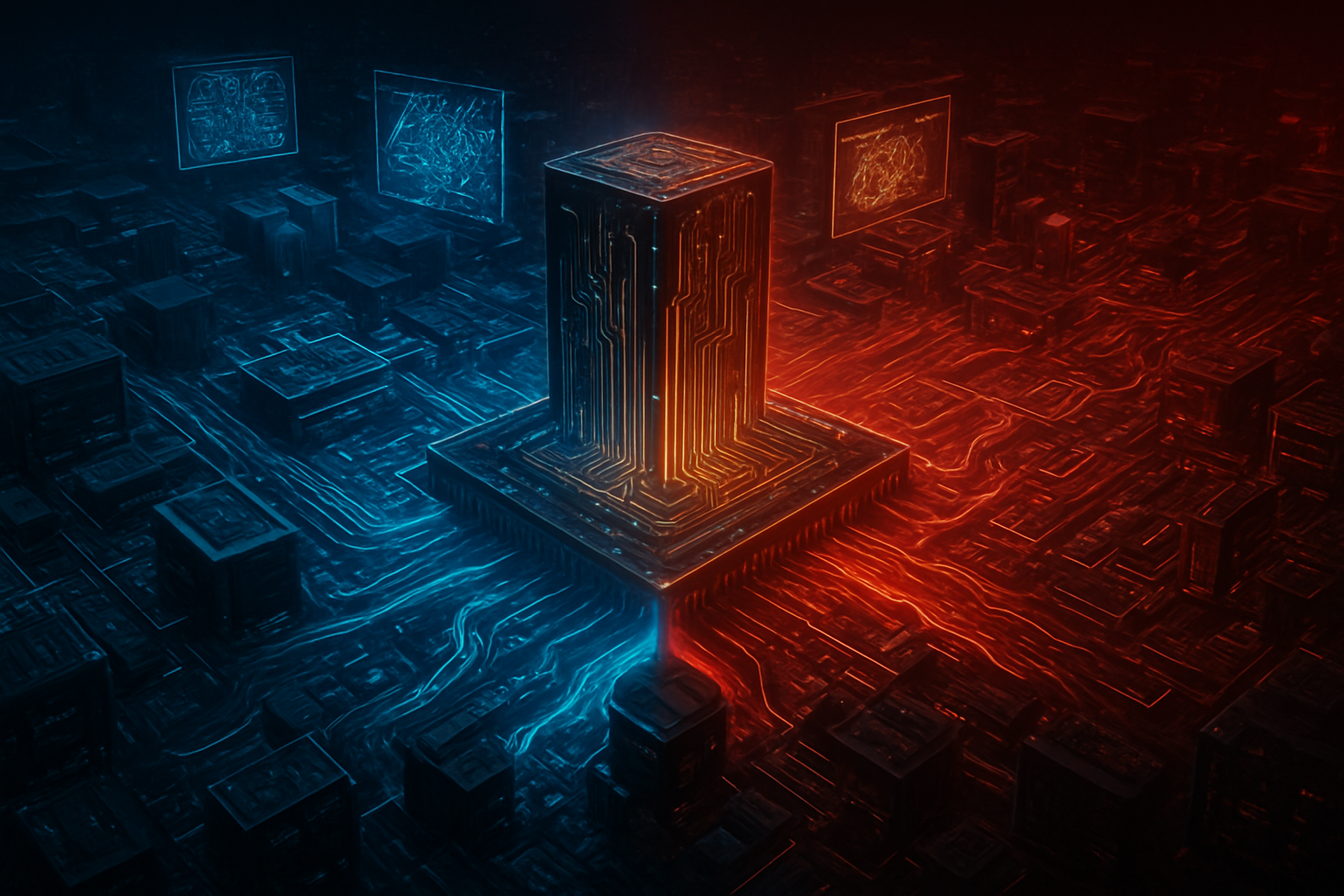
    The global technology landscape is witnessing a seismic shift as China intensifies its pursuit of semiconductor self-reliance, a strategic imperative underscored by the recent unveiling of Huawei's (SHE: 002502) Kirin 9030 chip. This advanced system-on-a-chip (SoC), powering Huawei's Mate 80 series smartphones, represents a significant stride in China's efforts to overcome stringent US export restrictions and establish an independent, robust domestic semiconductor ecosystem. Launched in late November 2025, the Kirin 9030 not only reasserts Huawei's presence in the premium smartphone segment but also sends a clear message about China's technological resilience and its unwavering commitment to leading the future of artificial intelligence.

    The immediate significance of the Kirin 9030 is multifaceted. It has already boosted Huawei's market share in China's premium smartphone segment, leveraging strong patriotic sentiment to reclaim ground from international competitors. More importantly, it demonstrates China's continued ability to advance its chipmaking capabilities despite being denied access to cutting-edge Extreme Ultraviolet (EUV) lithography machines. While a performance gap with global leaders like Taiwan Semiconductor Manufacturing Co (TSMC: TPE) and Samsung Electronics (KRX: 005930) persists, the chip's existence and adoption are a testament to China's growing prowess in advanced semiconductor manufacturing and its dedication to building an independent technological future.

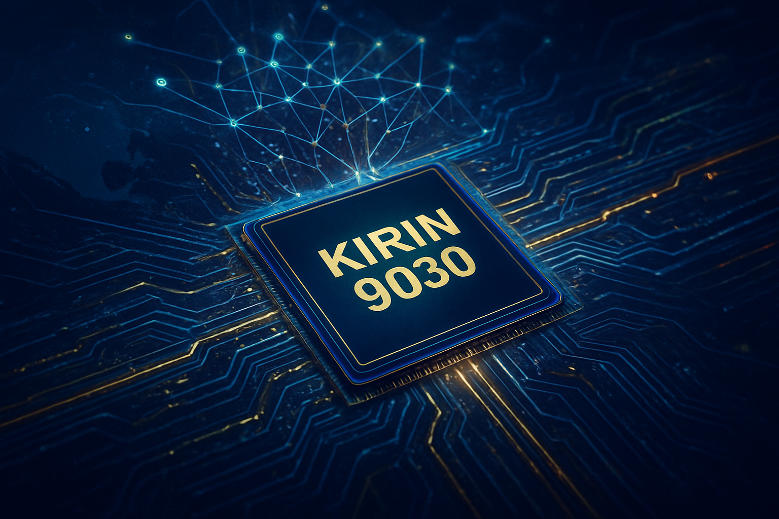
    Unpacking the Kirin 9030: A Technical Deep Dive into China's Chipmaking Prowess

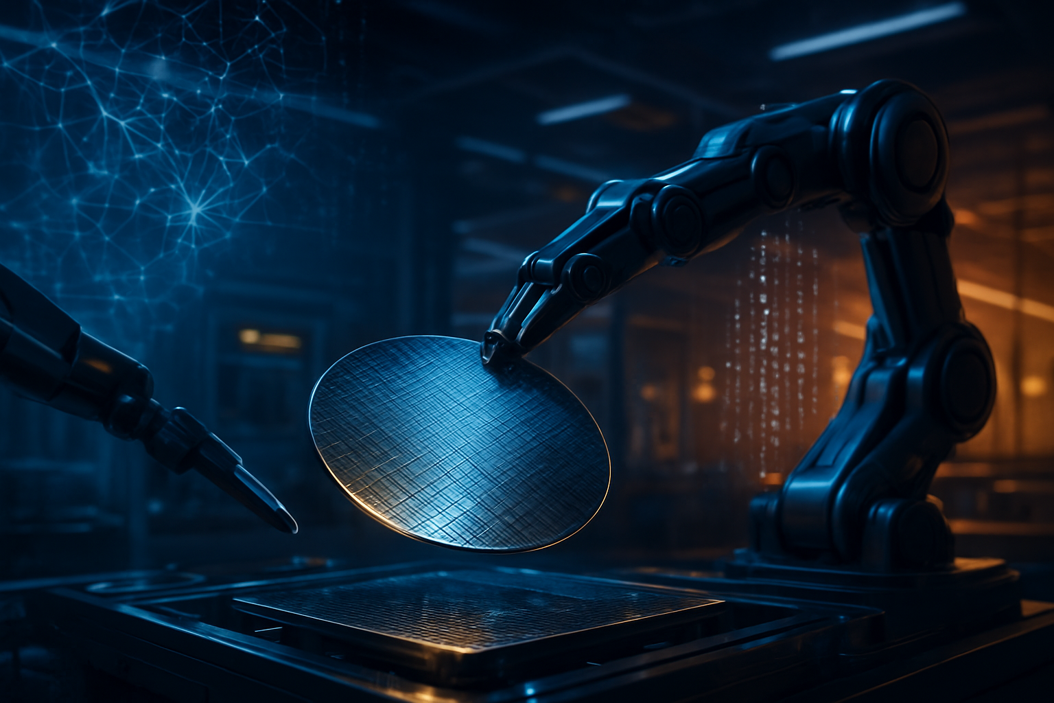
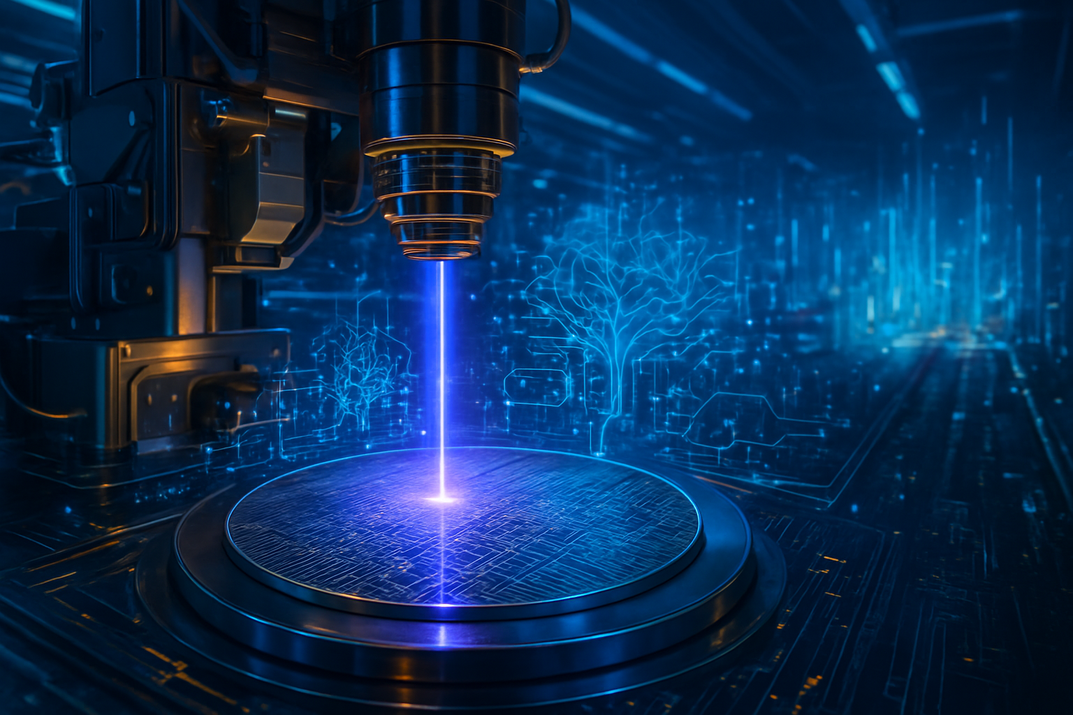
    The Huawei Kirin 9030, available in standard and Pro variants for the Mate 80 series, marks a pivotal achievement in China's domestic semiconductor journey. The chip is manufactured by Semiconductor Manufacturing International Corp (SMIC: SHA: 688981) using its N+3 fabrication process. TechInsights, a respected microelectronics research firm, confirms that SMIC's N+3 is a scaled evolution of its previous 7nm-class (N+2) node, placing it between 7nm and 5nm in terms of scaling and transistor density (approximately 125 Mtr/mm²). This innovative approach relies on Deep Ultraviolet (DUV) lithography combined with advanced multi-patterning and Design Technology Co-Optimization (DTCO), a workaround necessitated by US restrictions on EUV technology. However, this reliance on DUV multi-patterning for aggressively scaled metal pitches is expected to present significant yield challenges, potentially leading to higher manufacturing costs and constrained production volumes.

    The Kirin 9030 features a 9-core CPU configuration. The standard version boasts 12 threads, while the Pro variant offers 14 threads, indicating enhanced multi-tasking capabilities, likely through Simultaneous Multithreading (SMT). Both versions integrate a prime CPU core clocked at 2.75 GHz (likely a Taishan core), four performance cores at 2.27 GHz, and four efficiency cores at 1.72 GHz. The chip also incorporates the Maleoon 935 GPU, an upgrade from the Maleoon 920 in previous Kirin generations. Huawei claims a 35-42% performance improvement over its predecessor, the Kirin 9020, enabling advanced features like generative AI photography.

    Initial Geekbench 6 benchmark scores for the Kirin 9030 show a single-core score of 1,131 and a multi-core score of 4,277. These figures, while representing a significant leap for domestic manufacturing, indicate a performance gap compared to current flagship chipsets from global competitors. For instance, Apple's (NASDAQ: AAPL) A19 Pro achieves significantly higher scores, demonstrating a substantial advantage in single-threaded operations. Similarly, chips from Qualcomm (NASDAQ: QCOM) and MediaTek (TPE: 2454) show considerably faster results. Industry experts acknowledge Huawei's engineering ingenuity in advancing chip capabilities with DUV-based methods but also highlight that SMIC's N+3 process remains "substantially less scaled" than industry-leading 5nm processes. Huawei is strategically addressing hardware limitations through software optimization, such as its new AI infrastructure technology aiming for 70% GPU utilization, to bridge this performance gap.

    Compared to previous Kirin chips, the 9030's most significant difference is the leap to SMIC's N+3 process. It also introduces a 9-core CPU design, an advancement from the 8-core layout of the Kirin 9020, and an upgraded Maleoon 935 GPU. This translates to an anticipated 20% performance boost over the Kirin 9020 and promises improvements in battery efficiency, AI features, 5G connectivity stability, and heat management. The initial reaction from the AI research community and industry experts is a mix of admiration for Huawei's resilience and a realistic acknowledgment of the persistent technology gap. Within China, the Kirin 9030 is celebrated as a national achievement, a symbol of technological independence, while international analysts underscore the ingenuity required to achieve this progress under sanctions.

    Reshaping the AI Landscape: Implications for Tech Giants and Startups

    The advent of Huawei's Kirin 9030 and China's broader semiconductor advancements are profoundly reshaping the global AI industry, creating distinct advantages for Chinese companies while presenting complex competitive implications for international tech giants and startups.

    Chinese Companies: A Protected and Growing Ecosystem

    Chinese companies stand to be the primary beneficiaries. Huawei (SHE: 002502) itself gains a critical component for its advanced smartphones, reducing dependence on foreign supply chains and bolstering its competitive position. Beyond smartphones, Huawei's Ascend series chips are central to its data center AI strategy, complemented by its MindSpore deep learning framework. SMIC (SHA: 688981), as China's largest chipmaker, directly benefits from the national drive for self-sufficiency and increased domestic demand, exemplified by its role in manufacturing the Kirin 9030. Major tech giants like Baidu (NASDAQ: BIDU), Alibaba (NYSE: BABA), and Tencent (HKG: 0700) are heavily investing in AI R&D, developing their own AI models (e.g., Baidu's ERNIE 5.0) and chips (e.g., Baidu's Kunlun M100/M300, Alibaba's rival to Nvidia's H20). These companies benefit from a protected domestic market, vast internal data, strong state support, and a large talent pool, allowing for rapid innovation and scaling. AI chip startups such as Cambricon (SHA: 688256) and Moore Threads are also thriving under Beijing's push for domestic manufacturing, aiming to challenge global competitors.

    International Companies: Navigating a Fragmented Market

    For international players, the implications are more challenging. Nvidia (NASDAQ: NVDA), the global leader in AI hardware, faces significant challenges to its dominance in the Chinese market. While the US conditionally allows exports of Nvidia's H200 AI chips to China, Chinese tech giants and the government are reportedly rejecting these in favor of domestic alternatives, viewing them as a "sugar-coated bullet" designed to impede local growth. This highlights Beijing's strong resolve for semiconductor independence, even at the cost of immediate access to more advanced foreign technology. TSMC (TPE: 2330) and Samsung (KRX: 005930) remain leaders in cutting-edge manufacturing, but China's progress, particularly in mature nodes, could impact their long-term market share in certain segments. The strengthening of Huawei's Kirin line could also impact the market share of international mobile SoC providers like Qualcomm (NASDAQ: QCOM) and MediaTek (TPE: 2454) within China. The emergence of Chinese cloud providers expanding their AI services, such as Alibaba Cloud and Tencent Cloud, increases competition for global giants like Amazon Web Services and Microsoft (NASDAQ: MSFT) Azure.

    The broader impact includes a diversification of supply chains, with reduced reliance on foreign semiconductors affecting sales for international chipmakers. The rise of Huawei's MindSpore and other Chinese AI frameworks as alternatives to established platforms like PyTorch and Nvidia's CUDA could lead to a fragmented global AI software landscape. This competition is fueling a "tech cold war," where countries may align with different technological ecosystems, affecting global supply chains and potentially standardizing different technologies. China's focus on optimizing AI models for less powerful hardware also challenges the traditional "brute-force computing" approach, which could influence global AI development trends.

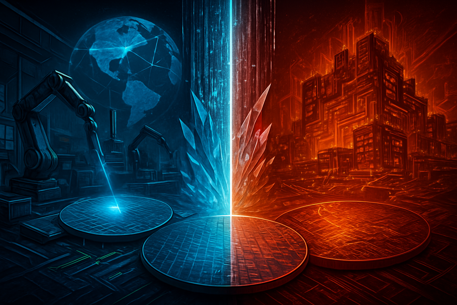
    A New Chapter in the AI Cold War: Wider Significance and Global Ramifications

    The successful development and deployment of Huawei's Kirin 9030 chip, alongside China's broader advancements in semiconductor manufacturing, marks a pivotal moment in the global technological landscape. This progress transcends mere economic competition, positioning itself squarely at the heart of an escalating "tech cold war" between the U.S. and China, with profound implications for artificial intelligence, geopolitics, and international supply chains.

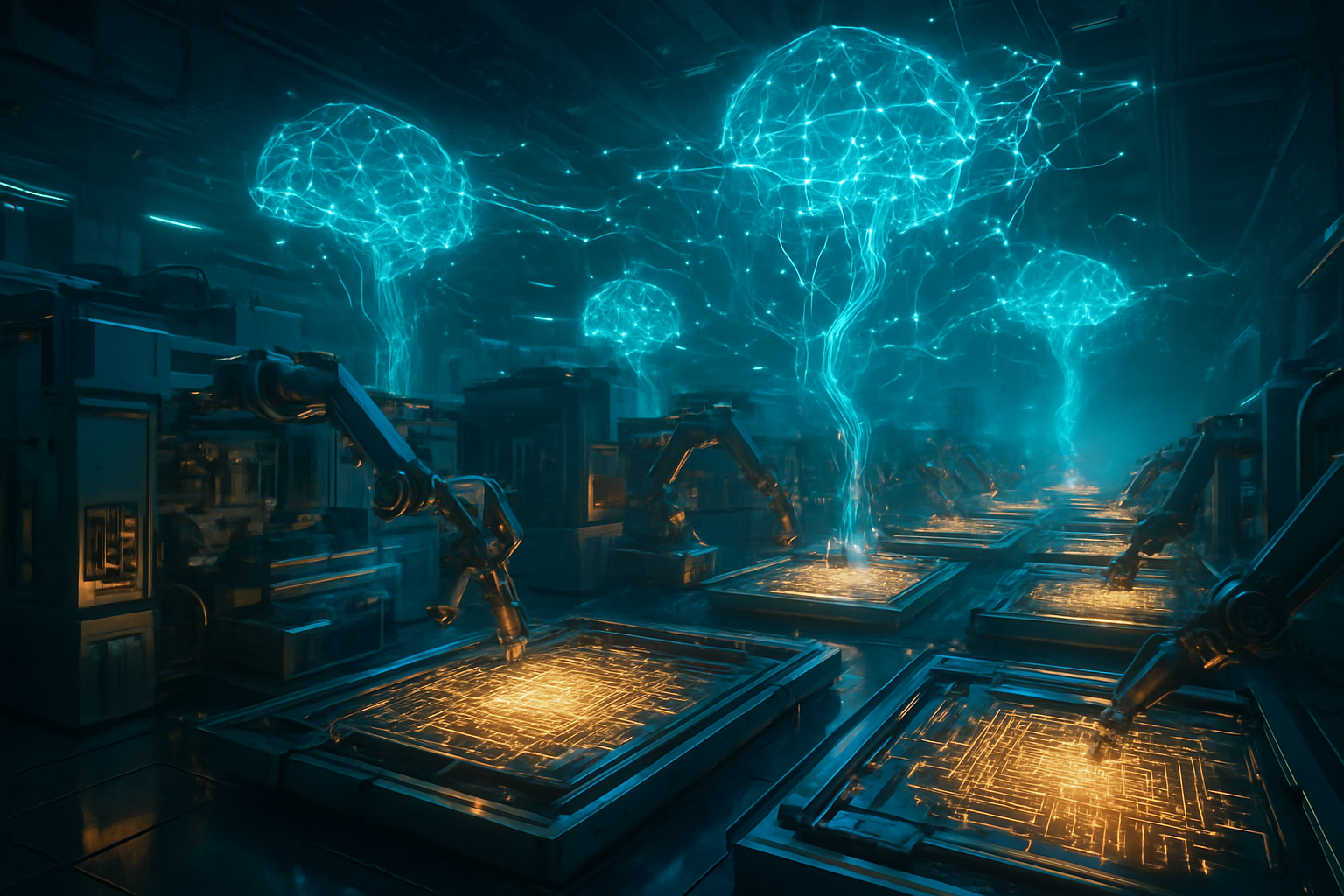
    The Kirin 9030 is a potent symbol of China's resilience under pressure. Produced by SMIC using DUV multi-patterning techniques without access to restricted EUV lithography, it demonstrates an impressive capacity for innovation and workaround solutions. This achievement validates China's strategic investment in domestic capabilities, aiming for 70% semiconductor import substitution by 2025 and 100% by 2030, backed by substantial government funding packages. In the broader AI landscape, this means China is actively building an independent AI hardware ecosystem, exemplified by Huawei's Ascend series chips and the company's focus on software innovations like new AI infrastructure technology to boost GPU utilization. This adaptive strategy, leveraging open-source AI models and specialized applications, helps optimize performance despite hardware constraints, driving innovation in AI applications.

    However, a considerable gap persists in cutting-edge AI chips compared to global leaders. While China's N+3 process is a testament to its resilience, it still lags behind the raw computing power of Nvidia's (NASDAQ: NVDA) H100 and upcoming B100/B200 chips, which are manufactured on more advanced 4nm and 3nm nodes by TSMC (TPE: 2330). This raw power is crucial for training the largest and most sophisticated AI models. The geopolitical impacts are stark: the Kirin 9030 reinforces the narrative of technological decoupling, leading to a fragmentation of global supply chains. US export controls and initiatives like the CHIPS and Science Act aim to reduce reliance on vulnerable chokepoints, while China's retaliatory measures, such as export controls on gallium and germanium, further disrupt these chains. This creates increased costs, potential inefficiencies, and a risk of missed market opportunities as companies are forced to navigate competing technological blocs.

    The emergence of parallel technology ecosystems, with both nations investing trillions in domestic production, affects national security, as advanced precision weapons and autonomous systems rely heavily on cutting-edge chips. China's potential to establish alternative norms and standards in AI and quantum computing could further fragment the global technology landscape. Compared to previous AI milestones, where breakthroughs were often driven by software algorithms and data availability, the current phase is heavily reliant on raw computing power from advanced semiconductors. While China's N+3 technology is a significant step, it underscores that achieving true leadership in AI requires both hardware and software prowess. China's focus on software optimization and practical AI applications, sometimes surpassing the U.S. in deployment scale, represents an alternative pathway that could redefine how AI progress is measured, shifting focus from raw chip power to optimized system efficiency and application-specific innovation.

    The Horizon of Innovation: Future Developments in China's AI and Semiconductor Journey

    As of December 15, 2025, China's semiconductor and AI sectors are poised for dynamic near-term and long-term developments, propelled by national strategic imperatives and a relentless pursuit of technological independence. The Kirin 9030 is but one chapter in this unfolding narrative, with ambitious goals on the horizon.

    In the near term (2025-2027), incremental yet meaningful progress in semiconductor manufacturing is expected. While SMIC's N+3 process, used for the Kirin 9030, is a DUV-based achievement, the company faces "significant yield challenges." However, domestic AI chip production is seeing rapid growth, with Chinese homegrown AI chips capturing over 50% market share in Chinese data centers by late 2024. Huawei (SHE: 002502) is projected to secure 50% of the Chinese AI chip market by 2026, aiming to address production bottlenecks through its own fab buildout. Notably, Shanghai Micro Electronics Equipment (SMEE) plans to commence manufacturing 28nm chip-making machines in early 2025, crucial for various applications. China also anticipates trial production of its domestic EUV system, utilizing Laser-induced Discharge Plasma (LDP) technology, by Q3 2025, with mass production slated for 2026. On the AI front, China's "AI Plus" initiative aims for deep AI integration across six key domains by 2027, targeting adoption rates for intelligent terminals and agents exceeding 70%, with the core AI industry projected to surpass $140 billion in 2025.

    Looking further ahead (2028-2035), China's long-term semiconductor strategy focuses on achieving self-reliance and global competitiveness. Experts predict that successful commercialization of domestic EUV technology could enable China to advance to 3nm or 2nm chip production by 2030, potentially challenging ASML (AMS: ASML), TSMC (TPE: 2330), and Samsung (KRX: 005930). This is supported by substantial government investment, including a $47 billion fund established in May 2024. Huawei is also establishing a major R&D center for exposure and wafer fabrication equipment, underscoring long-term commitment to domestic toolmaking. By 2030, China envisions adoption rates of intelligent agents and terminals exceeding 90%, with the "intelligent economy" becoming a primary driver of growth. By 2035, AI is expected to form the backbone of intelligent economic and social development, transforming China into a leading global AI innovation hub.

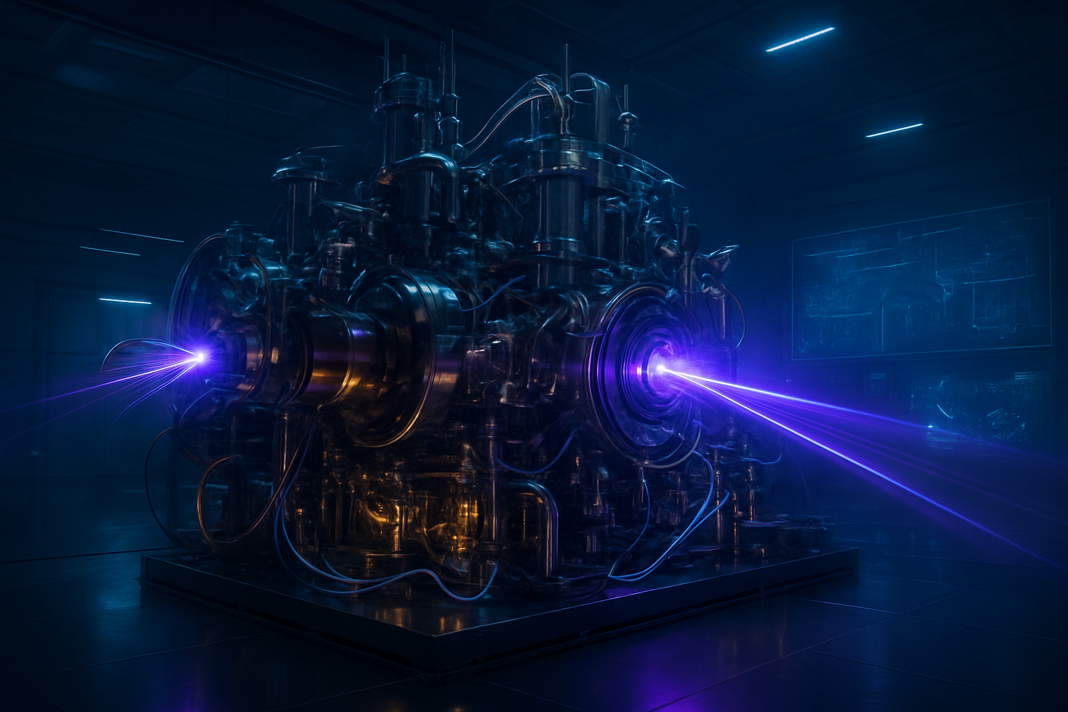
    Potential applications and use cases on the horizon are vast, spanning intelligent manufacturing, enhanced consumer electronics (e.g., generative AI photography, AI glasses), the continued surge in AI-optimized data centers, and advanced autonomous systems. AI integration into public services, healthcare, and scientific research is also a key focus. However, significant challenges remain. The most critical bottleneck is EUV access, forcing reliance on less efficient DUV multi-patterning, leading to "significant yield challenges." While China is developing its own LDP-based EUV technology, achieving sufficient power output and integrating it into mass production are hurdles. Access to advanced Electronic Design Automation (EDA) tools also remains a challenge. Expert predictions suggest China is catching up "faster than expected," with some attributing this acceleration to US sanctions "backfiring." China's AI chip supply is predicted to surpass domestic demand by 2028, hinting at potential exports and the formation of an "AI 'Belt & Road' Initiative." The "chip war" is expected to persist for decades, shaping an ongoing geopolitical and technological struggle.

    A Defining Moment: Assessing China's AI and Semiconductor Trajectory

    The unveiling of Huawei's (SHE: 002502) Kirin 9030 chip and China's broader progress in semiconductor manufacturing mark a defining moment in the history of artificial intelligence and global technology. This development is not merely about a new smartphone chip; it symbolizes China's remarkable resilience, strategic foresight, and unwavering commitment to technological self-reliance in the face of unprecedented international pressure. As of December 15, 2025, the narrative is clear: China is actively forging an independent AI ecosystem, reducing its vulnerability to external geopolitical forces, and establishing alternative pathways for innovation.

    The key takeaways from this period are profound. The Kirin 9030, produced by SMIC (SHA: 688981) using its N+3 process, demonstrates China's ability to achieve "5nm-grade" performance without access to advanced EUV lithography, a testament to its engineering ingenuity. This has enabled Huawei to regain significant market share in China's premium smartphone segment and integrate advanced AI capabilities, such as generative AI photography, into consumer devices using domestically sourced hardware. More broadly, China's semiconductor progress is characterized by massive state-backed investment, significant advancements in manufacturing nodes (even if behind the absolute cutting edge), and a strategic focus on localizing the entire semiconductor supply chain, from design to equipment. The reported rejection of Nvidia's (NASDAQ: NVDA) H200 AI chips in favor of domestic alternatives further underscores China's resolve to prioritize independence over immediate access to foreign technology.

    In the grand tapestry of AI history, this development signifies the laying of a foundational layer for independent AI ecosystems. By developing increasingly capable domestic chips, China ensures its AI development is not bottlenecked or dictated by foreign technology, allowing it to control its own AI hardware roadmap and foster unique AI innovations. This strategic autonomy in AI, particularly for powering large language models and complex machine learning, is crucial for national security and economic competitiveness. The long-term impact will likely lead to an accelerated technological decoupling, with the emergence of two parallel technological ecosystems, each with its own supply chains, standards, and innovations. This will have significant geopolitical implications, potentially altering the balance of technological and economic power globally, and redirecting innovation towards novel approaches in chip design, manufacturing, and AI system architecture under constraint.

    In the coming weeks and months, several critical developments warrant close observation. Detailed independent reviews and teardowns of the newly launched Huawei Mate 80 series will provide concrete data on the Kirin 9030's real-world performance and manufacturing process. Reports on SMIC's ability to produce the Kirin 9030 and subsequent chips at scale with economically viable yields will be crucial. We should also watch for further announcements and evidence of progress regarding Huawei's plans to open dedicated AI chip production facilities by the end of 2025 and into 2026. The formal approval of China's 15th Five-Year Plan (2026-2030) in March 2026 will unveil more specific goals and funding for advanced semiconductor and AI development. The actual market dynamics and uptake of domestic AI chips in China, especially in data centers, following the reported rejection of Nvidia's H200, will indicate the effectiveness of China's "semiconductor independence" strategy. Finally, any further reported breakthroughs in Chinese-developed lithography techniques or the widespread deployment of advanced Chinese-made etching, deposition, and testing equipment will signal accelerating self-sufficiency across the entire supply chain, marking a new chapter in the global technology race.


    This content is intended for informational purposes only and represents analysis of current AI developments.

    TokenRing AI delivers enterprise-grade solutions for multi-agent AI workflow orchestration, AI-powered development tools, and seamless remote collaboration platforms.
    For more information, visit https://www.tokenring.ai/.