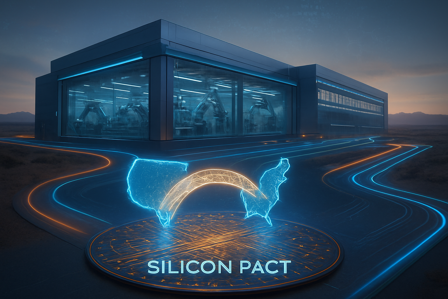
Tag: Supply Chain

  • The Great AI Detour: Trump’s New Chip Tariffs and the 180-Day Countdown for Critical Minerals

    The Great AI Detour: Trump’s New Chip Tariffs and the 180-Day Countdown for Critical Minerals

    As the new administration enters its second year, a series of aggressive trade maneuvers has sent shockwaves through the global technology sector. On January 13, 2026, the White House codified a landmark "U.S. Detour" protocol for high-performance AI semiconductors, fundamentally altering how companies like Nvidia (NASDAQ:NVDA) and AMD (NASDAQ:AMD) access the Chinese market. This policy shift, characterized by a transition from broad Biden-era prohibitions to a "monetized export" model, effectively forces advanced chips manufactured abroad to route through U.S. soil for mandatory laboratory verification before they can be shipped to restricted destinations.

    The announcement was followed just 24 hours later by a sweeping executive proclamation targeting the "upstream" supply chain. President Trump has established a strict 180-day deadline—falling on July 13, 2026—for the United States to secure binding agreements with global allies to diversify away from Chinese-processed critical minerals. If these negotiations fail to yield a non-Chinese supply chain for the rare earth elements essential to AI hardware, the administration is authorized to impose unilateral "remedial" tariffs and minimum import prices. Together, these moves represent a massive escalation in the geopolitical struggle for AI supremacy, framed within the industry as a definitive realization of "Item 23" on the global risk index: Supply Chain Trade Impacts.

    A Technical Toll Bridge: The 'U.S. Detour' Protocol

    The technical crux of the new policy lies in the physical and performance-based verification of mid-to-high performance AI hardware. Under the new Bureau of Industry and Security (BIS) guidelines, chips equivalent to the Nvidia H200 and AMD MI325X—previously operating under a cloud of regulatory uncertainty—are now permitted for export to China, but only under a rigorous "detour" mandate. Every shipment must be physically routed through an independent, U.S.-headquartered laboratory. These labs must certify that the hardware’s Total Processing Performance (TPP) remains below a strict cap of 21,000, and its total DRAM bandwidth does not exceed 6,500 GB/s.

    This "detour" serves two purposes: physical security and financial leverage. By requiring chips manufactured at foundries like TSMC in Taiwan to enter U.S. customs territory, the administration is able to apply a 25% Section 232 tariff on the hardware as it enters the country, and an additional "export fee" as it departs. This effectively treats the chips as a double-taxed commodity, generating an estimated $4 billion in annual revenue for the U.S. Treasury. Furthermore, the protocol mandates a "Shipment Ratio," where total exports of a specific chip model to restricted jurisdictions cannot exceed 50% of the volume sold to domestic U.S. customers, ensuring that American firms always maintain a superior compute-to-export ratio.

    Industry experts and the AI research community have expressed a mix of relief and concern. While the policy provides a legal "release valve" for Nvidia to sell its H200 chips to Chinese tech giants like Alibaba (NYSE:BABA) and ByteDance, the logistical friction of a U.S. detour is unprecedented. "We are essentially seeing the creation of a technical toll bridge for the AI era," noted one senior researcher at the Center for AI Standards and Innovation (CAISI). "It provides clarity, but at the cost of immense supply chain latency and a significant 'Trump Tax' on global silicon."

    Market Rerouting: Winners, Losers, and Strategic Realignment

    The implications for major tech players are profound. For Nvidia and AMD, the policy is a double-edged sword. While it reopens a multi-billion dollar revenue stream from China that had been largely throttled by 2024-era bans, the 25% premium makes their products significantly more expensive than domestic Chinese alternatives. This has provided an unexpected opening for Huawei’s Ascend 910C series, which Beijing is now aggressively subsidizing to counteract the high cost of American "detour" chips. Nvidia, in particular, must now manage a "whiplash" logistics network that moves silicon from Taiwan to the U.S. for testing, and then back across the Pacific to Shenzhen.

    In the cloud sector, companies like Amazon (NASDAQ:AMZN) and Microsoft (NASDAQ:MSFT) stand to benefit from the administration's "AI Action Plan," which prioritizes domestic data center hardening and provides $1.6 billion in new incentives for "high-security compute environments." However, the "Cloud Disclosure" requirement—forcing providers to list all remote end-users in restricted jurisdictions—has created a compliance nightmare for startups attempting to build global platforms. The strategic advantage has shifted toward firms that can prove a "purely American" hardware-software stack, free from the logistical and regulatory risks of the China trade.

    Conversely, the market is already pricing in the risk of the July 180-day deadline. Critical mineral processors and junior mining companies in Australia, Saudi Arabia, and Canada have seen a surge in investment as they race to become the "vetted alternatives" to Chinese suppliers. Companies that fail to diversify their mineral sourcing by mid-summer 2026 face the prospect of being locked out of the U.S. market or hit with debilitating secondary tariffs.

    Geopolitical Fallout and the 'Item 23' Paradigm

    The broader significance of these policies lies in their departure from traditional trade diplomacy. By monetizing export controls through fees and tariffs, the administration has turned national security regulations into a tool for industrial policy. This aligns with "Item 23" of the global AI outlook: Supply Chain Trade Impacts. This paradigm shift suggests that the era of "just-in-time" globalized AI manufacturing is officially over, replaced by a "Fortress America" model that seeks to decouple the U.S. AI stack from Chinese influence at every level—from the minerals in the ground to the weights of the models.

    Critics argue that this "monetized protectionism" could backfire by accelerating China’s drive for self-reliance. Beijing’s response has been to leverage its dominance in processed gallium and germanium, essentially holding the 180-day deadline over the head of the U.S. tech industry. If the U.S. cannot secure enough non-Chinese supply by July 13, 2026, the resulting shortages could spike the price of AI servers globally, potentially stalling the very "AI revolution" the administration seeks to lead. This echoes previous milestones like the 1980s semiconductor wars with Japan, but with the added complexity of a resource-starved supply chain.

    Furthermore, the administration's move to strip "ideological bias" from the NIST AI Risk Management Framework marks a cultural shift in AI governance. By refocusing on technical robustness and performance over social metrics, the U.S. is signaling a preference for "objective" frontier models, a move that has been welcomed by some in the defense sector but viewed with skepticism by ethics researchers who fear a "race to the bottom" in safety standards.

    The Road to July: What Happens Next?

    In the near term, all eyes are on the Department of State and the USTR as they scramble to finalize "Prosperity Deals" with Saudi Arabia and Malaysia to secure alternative mineral processing hubs. These negotiations are fraught with difficulty, as these nations must weigh the benefits of U.S. partnership against the risk of alienating China, their primary trade partner. Meanwhile, the AI Overwatch Act currently moving through Congress could introduce further volatility; if passed, it would give the House a veto over individual Nvidia export licenses, potentially overriding the administration's "revenue-sharing" model.

    Technologically, we expect to see a surge in R&D focused on "mineral-agnostic" hardware. Researchers are already exploring alternative substrates for high-performance computing that minimize the use of rare earth elements, though these technologies are likely years away from commercial viability. In the meantime, the "U.S. Detour" will become the standard operating procedure for the industry, with massive testing facilities currently being constructed in logistics hubs like Memphis and Dallas to handle the influx of Pacific-bound silicon.

    The prediction among most industry analysts is that the July deadline will lead to a "Partial Decoupling Agreement." The U.S. is likely to secure enough supply to protect its military and critical infrastructure compute, while consumer-grade AI hardware remains subject to the volatile swings of the trade war. The ultimate challenge will be maintaining the pace of AI innovation while simultaneously rebuilding a century-old global supply chain in less than six months.

    Summary of the 2026 AI Trade Landscape

    The developments of January 2026 mark a definitive turning point in the history of artificial intelligence. By implementing the "U.S. Detour" protocol and setting a hard 180-day deadline for critical minerals, the Trump administration has effectively weaponized the AI supply chain. The key takeaways for the industry are clear: market access is now a paid privilege, technical specifications are subject to physical verification on U.S. soil, and mineral dependency is the primary vulnerability of the digital age.

    The significance of these moves cannot be overstated. We have moved beyond "chips wars" into a "full-stack" geopolitical confrontation. As we look toward the July 13 deadline, the resilience of the U.S. AI ecosystem will be put to its ultimate test. Stakeholders should watch for the first "U.S. Detour" certifications in late February and keep a close eye on the diplomatic progress of mineral-sourcing treaties in the Middle East and Southeast Asia. The future of AI is no longer just about who has the best algorithms; it’s about who controls the dirt they are built on and the labs they pass through.


    This content is intended for informational purposes only and represents analysis of current AI developments.

    TokenRing AI delivers enterprise-grade solutions for multi-agent AI workflow orchestration, AI-powered development tools, and seamless remote collaboration platforms.
    For more information, visit https://www.tokenring.ai/.

  • Silicon Sovereignty: The High Cost and Hard Truths of Reshoring the Global Chip Supply

    Silicon Sovereignty: The High Cost and Hard Truths of Reshoring the Global Chip Supply

    As of January 27, 2026, the ambitious dream of the U.S. CHIPS and Science Act has transitioned from legislative promise to a complex, grit-and-mortar reality. While the United States has successfully spurred the largest industrial reshoring effort in half a century, the path to domestic semiconductor self-sufficiency has been marred by stark "efficiency gaps," labor friction, and massive cost overruns. The effort to bring advanced logic chip manufacturing back to American soil is no longer just a policy goal; it is a high-stakes stress test of the nation's industrial capacity and its ability to compete with the hyper-efficient manufacturing ecosystems of East Asia.

    The immediate significance of this transition cannot be overstated. With Intel Corporation (NASDAQ:INTC) recently announcing high-volume manufacturing (HVM) of its 18A (1.8nm-class) node in Arizona, and Taiwan Semiconductor Manufacturing Company (NYSE:TSM) reaching high-volume production for 3nm at its Phoenix site, the U.S. has officially broken its reliance on foreign soil for the world's most advanced processors. However, this "Silicon Sovereignty" comes with a caveat: building and operating these facilities in the U.S. remains significantly more expensive and time-consuming than in Taiwan, forcing a massive realignment of the global supply chain that is already impacting the pricing of everything from AI servers to consumer electronics.

    The technical landscape of January 2026 is defined by a fierce race for the 2-nanometer (2nm) threshold. In Taiwan, TSMC has already achieved high-volume manufacturing of its N2 nanosheet process at its "mother fabs" in Hsinchu and Kaohsiung, boasting yields between 70% and 80%. In contrast, while Intel’s 18A process has reached the HVM stage in Arizona, initial yields are estimated at a more modest 60%, highlighting the lingering difficulty of stabilizing leading-edge nodes outside of the established Taiwanese ecosystem. Samsung Electronics Co., Ltd. (KRX:005930) has also pivoted, skipping its initial 4nm plans for its Taylor, Texas facility to install 2nm (SF2) equipment directly, though mass production there is not expected until late 2026.

    The "efficiency gap" between the two regions remains the primary technical and economic hurdle. Data from early 2026 shows that while a fab shell in Taiwan can be completed in approximately 20 to 28 months, a comparable facility in the U.S. takes between 38 and 60 months. Construction costs in the U.S. are nearly double, ranging from $4 billion to $6 billion per fab shell compared to $2 billion to $3 billion in Hsinchu. While semiconductor equipment from providers like ASML (NASDAQ:ASML) and Applied Materials (NASDAQ:AMAT) is priced globally—keeping total wafer processing costs to a manageable 10–15% premium in the U.S.—the sheer capital expenditure (CAPEX) required to break ground is staggering.

    Industry experts note that these delays are often tied to the "cultural clash" of manufacturing philosophies. Throughout 2025, several high-profile labor disputes surfaced, including a class-action lawsuit against TSMC Arizona regarding its reliance on Taiwanese "transplant" workers to maintain a 24/7 "war room" work culture. This culture, which is standard in Taiwan’s Science Parks, has met significant resistance from the American workforce, which prioritizes different work-life balance standards. These frictions have directly influenced the speed at which equipment can be calibrated and yields can be optimized.

    The impact on major tech players is a study in strategic navigation. For companies like NVIDIA Corporation (NASDAQ:NVDA) and Apple Inc. (NASDAQ:AAPL), the reshoring effort provides a "dual-source" security blanket but introduces new pricing pressures. In early 2026, the U.S. government imposed a 25% Section 232 tariff on advanced AI chips not manufactured or packaged on U.S. soil. This move has effectively forced NVIDIA to prioritize U.S.-made silicon for its latest "Rubin" architecture, ensuring that its primary domestic customers—including government agencies and major cloud providers—remain compliant with new "secure supply" mandates.

    Intel stands as a major beneficiary of the CHIPS Act, having reclaimed a temporary title of "process leadership" with its 18A node. However, the company has had to scale back its "Silicon Heartland" project in Ohio, delaying the completion of its first two fabs to 2030 to align with market demand and capital constraints. This strategic pause has allowed competitors to catch up, but Intel’s position as the primary domestic foundry for the U.S. Department of Defense remains a powerful competitive advantage. Meanwhile, fabless firms like Advanced Micro Devices, Inc. (NASDAQ:AMD) are navigating a split strategy, utilizing TSMC’s Arizona capacity for domestic needs while keeping their highest-volume, cost-sensitive production in Taiwan.

    The shift has also birthed a new ecosystem of localized suppliers. Over 75 tier-one suppliers, including Amkor Technology, Inc. (NASDAQ:AMKR) and Tokyo Electron, have established regional hubs in Phoenix, creating a "Silicon Desert" that mirrors the density of Taiwan’s Hsinchu Science Park. This migration is essential for reducing the "latencies of distance" that plagued the supply chain during the early 2020s. However, smaller startups are finding it harder to compete in this high-cost environment, as the premium for U.S.-made silicon often eats into the thin margins of new hardware ventures.

    This development aligns directly with Item 21 of our top 25 list: the reshoring of advanced manufacturing. The reality of 2026 is that the global supply chain is no longer optimized solely for "just-in-time" efficiency, but for "just-in-case" resilience. The "Silicon Shield"—the theory that Taiwan’s dominance in chips prevents geopolitical conflict—is being augmented by a "Silicon Fortress" in the U.S. This shift represents a fundamental rejection of the hyper-globalized model that dominated the last thirty years, favoring a fragmented, "friend-shored" system where manufacturing is tied to national security alliances.

    The wider significance of this reshoring effort also touches on the accelerating demand for AI infrastructure. As AI models grow in complexity, the chips required to train them have become strategic assets on par with oil or grain. By reshoring the manufacturing of these chips, the U.S. is attempting to insulate its AI-driven economy from potential blockades or regional conflicts in the Taiwan Strait. However, this move has raised concerns about "technology inflation," as the higher costs of domestic production are inevitably passed down to the end-users of AI services, potentially widening the gap between well-funded tech giants and smaller players.

    Comparisons to previous industrial milestones, such as the space race or the build-out of the interstate highway system, are common among policymakers. However, the semiconductor industry is unique in its pace of change. Unlike a road or a bridge, a $20 billion fab can become obsolete in five years if the technology node it supports is surpassed. This creates a "permanent investment trap" where the U.S. must not only build these fabs but continually subsidize their upgrades to prevent them from becoming expensive relics of a previous generation of technology.

    Looking ahead, the next 24 months will be focused on the deployment of 1.4-nanometer (1.4nm) technology and the maturation of advanced packaging. While the U.S. has made strides in wafer fabrication, "backend" packaging remains a bottleneck, with the majority of the world's advanced chip-stacking capacity still located in Asia. To address this, expect a new wave of CHIPS Act grants specifically targeting companies like Amkor and Intel to build out "Substrate-to-System" facilities that can package chips domestically.

    Labor remains the most significant long-term challenge. Experts predict that by 2028, the U.S. semiconductor industry will face a shortage of over 60,000 technicians and engineers. To combat this, several "Semiconductor Academies" have been launched in Arizona and Ohio, but the timeline for training a specialized workforce often exceeds the timeline for building a fab. Furthermore, the industry is closely watching the implementation of Executive Order 14318, which aims to streamline environmental reviews for chip projects. If these regulatory reforms fail to stick, future fab expansions could be stalled for years in the courts.

    Near-term developments will likely include more aggressive trade deals. The landmark agreement signed on January 15, 2026, between the U.S. and Taiwan—which exchanged massive Taiwanese investment for tariff caps—is expected to be a blueprint for future deals with Japan and South Korea. These "Chip Alliances" will define the geopolitical landscape for the remainder of the decade, as nations scramble to secure their place in the post-globalized semiconductor hierarchy.

    In summary, the reshoring of advanced manufacturing via the CHIPS Act has reached a pivotal, albeit difficult, success. The U.S. has proven it can build leading-edge fabs and produce the world's most advanced silicon, but it has also learned that the "Taiwan Advantage"—a combination of hyper-efficient labor, specialized infrastructure, and government prioritization—cannot be replicated overnight or through capital alone. The reality of 2026 is a bifurcated world where the U.S. serves as the secure, high-cost "fortress" for chip production, while Taiwan remains the efficient, high-yield "brain" of the industry.

    The long-term impact of this development will be felt in the resilience of the AI economy. By decoupling the most critical components of the tech stack from a single geographic point of failure, the U.S. has significantly mitigated the risk of a total supply chain collapse. However, the cost of this insurance is high, manifesting in higher hardware prices and a permanent need for government industrial policy.

    As we move into the second half of 2026, watch for the first yield reports from Samsung’s Taylor fab and the progress of Intel’s 14A node development. These will be the true indicators of whether the U.S. can sustain its momentum or if the high costs of reshoring will eventually lead to a "silicon fatigue" that slows the pace of domestic innovation.


    This content is intended for informational purposes only and represents analysis of current AI developments.

    TokenRing AI delivers enterprise-grade solutions for multi-agent AI workflow orchestration, AI-powered development tools, and seamless remote collaboration platforms.
    For more information, visit https://www.tokenring.ai/.

  • The CoWoS Stranglehold: TSMC Ramps Advanced Packaging as AI Demand Outpaces the Physics of Supply

    The CoWoS Stranglehold: TSMC Ramps Advanced Packaging as AI Demand Outpaces the Physics of Supply

    As of late January 2026, the artificial intelligence industry finds itself in a familiar yet intensified paradox: despite a historic, multi-billion-dollar expansion of semiconductor manufacturing capacity, the "Compute Crunch" remains the defining characteristic of the tech landscape. At the heart of this struggle is Taiwan Semiconductor Manufacturing Co. (TPE: 2330) and its Chip-on-Wafer-on-Substrate (CoWoS) advanced packaging technology. While TSMC has successfully quadrupled its CoWoS output compared to late 2024 levels, the insatiable hunger of generative AI models has kept the supply chain in a state of perpetual "catch-up," making advanced packaging the ultimate gatekeeper of global AI progress.

    This persistent bottleneck is the physical manifestation of Item 9 on our Top 25 AI Developments list: The Infrastructure Ceiling. As AI models shift from the trillion-parameter Blackwell era into the multi-trillion-parameter Rubin era, the limiting factor is no longer just how many transistors can be etched onto a wafer, but how many high-bandwidth memory (HBM) modules and logic dies can be fused together into a single, high-performance package.

    The Technical Frontier: Beyond Simple Silicon

    The current state of CoWoS in early 2026 is a far cry from the nascent stages of two years ago. TSMC’s AP6 facility in Zhunan is now operating at peak capacity, serving as the workhorse for NVIDIA's (NASDAQ: NVDA) Blackwell series. However, the technical specifications have evolved. We are now seeing the widespread adoption of CoWoS-L, which utilizes local silicon interconnects (LSI) to bridge chips, allowing for larger package sizes that exceed the traditional "reticle limit" of a single chip.

    Technical experts point out that the integration of HBM4—the latest generation of High Bandwidth Memory—has added a new layer of complexity. Unlike previous iterations, HBM4 requires a more intricate 2048-bit interface, necessitating the precision that only TSMC’s advanced packaging can provide. This transition has rendered older "on-substrate" methods obsolete for top-tier AI training, forcing the entire industry to compete for the same limited CoWoS-L and SoIC (System on Integrated Chips) lines. The industry reaction has been one of cautious awe; while the throughput of these packages is unprecedented, the yields for such complex "chiplets" remain a closely guarded secret, frequently cited as the reason for the continued delivery delays of enterprise-grade AI servers.

    The Competitive Arena: Winners, Losers, and the Arizona Pivot

    The scarcity of CoWoS capacity has created a rigid hierarchy in the tech sector. NVIDIA remains the undisputed king of the queue, reportedly securing nearly 60% of TSMC’s total 2026 capacity to fuel its transition to the Rubin (R100) architecture. This has left rivals like AMD (NASDAQ: AMD) and custom silicon giants like Broadcom (NASDAQ: AVGO) and Marvell Technology (NASDAQ: MRVL) in a fierce battle for the remaining slots. For hyperscalers like Google and Amazon, who are increasingly designing their own AI accelerators (TPUs and Trainium), the CoWoS bottleneck represents a strategic risk that has forced them to diversify their packaging partners.

    To mitigate this, a landmark collaboration has emerged between TSMC and Amkor Technology (NASDAQ: AMKR). In a strategic move to satisfy U.S. "chips-act" requirements and provide geographical redundancy, the two firms have established a turnkey advanced packaging line in Peoria, Arizona. This allows TSMC to perform the front-end "Chip-on-Wafer" process in its Phoenix fabs while Amkor handles the "on-Substrate" finishing nearby. While this has provided a pressure valve for North American customers, it has not yet solved the global shortage, as the most advanced "Phase 1" of TSMC’s massive AP7 plant in Chiayi, Taiwan, has faced minor delays, only just beginning its equipment move-in this quarter.

    A Wider Significance: Packaging is the New Moore’s Law

    The CoWoS saga underscores a fundamental shift in the semiconductor industry. For decades, progress was measured by the shrinking size of transistors. Today, that progress has shifted to "More than Moore" scaling—using advanced packaging to stack and stitch together multiple chips. This is why advanced packaging is now a primary revenue driver, expected to contribute over 10% of TSMC’s total revenue by the end of 2026.

    However, this shift brings significant geopolitical and environmental concerns. The concentration of advanced packaging in Taiwan remains a point of vulnerability for the global AI economy. Furthermore, the immense power requirements of these multi-die packages—some consuming over 1,000 watts per unit—have pushed data center cooling technologies to their limits. Comparisons are often drawn to the early days of the jet engine: we have the power to reach incredible speeds, but the "materials science" of the engine (the package) is now the primary constraint on how fast we can go.

    The Road Ahead: Panel-Level Packaging and Beyond

    Looking toward the horizon of 2027 and 2028, TSMC is already preparing for the successor to CoWoS: CoPoS (Chip-on-Panel-on-Substrate). By moving from circular silicon wafers to large rectangular glass panels, TSMC aims to increase the area of the packaging surface by several multiples, allowing for even larger "AI Super-Chips." Experts predict this will be necessary to support the "Rubin Ultra" chips expected in late 2027, which are rumored to feature even more HBM stacks than the current Blackwell-Ultra configurations.

    The challenge remains the "yield-to-complexity" ratio. As packages become larger and more complex, the chance of a single defect ruining a multi-thousand-dollar assembly increases. The industry is watching closely to see if TSMC’s Arizona AP1 facility, slated for construction in the second half of this year, can replicate the high yields of its Taiwanese counterparts—a feat that has historically proven difficult.

    Wrapping Up: The Infrastructure Ceiling

    In summary, TSMC’s Herculean efforts to ramp CoWoS capacity to 120,000+ wafers per month by early 2026 are a testament to the company's engineering prowess, yet they remain insufficient against the backdrop of the global AI gold rush. The bottleneck has shifted from "can we make the chip?" to "can we package the system?" This reality cements Item 9—The Infrastructure Ceiling—as the most critical challenge for AI developers today.

    As we move through 2026, the key indicators to watch will be the operational ramp of the Chiayi AP7 plant and the success of the Amkor-TSMC Arizona partnership. For now, the AI industry remains strapped to the pace of TSMC’s cleanrooms. The long-term impact is clear: those who control the packaging, control the future of artificial intelligence.


    This content is intended for informational purposes only and represents analysis of current AI developments.

    TokenRing AI delivers enterprise-grade solutions for multi-agent AI workflow orchestration, AI-powered development tools, and seamless remote collaboration platforms.
    For more information, visit https://www.tokenring.ai/.

  • India’s Silicon Shield: How the Tata-ROHM Alliance is Rewriting the Global Semiconductor and AI Power Map

    India’s Silicon Shield: How the Tata-ROHM Alliance is Rewriting the Global Semiconductor and AI Power Map

    As of January 26, 2026, the global semiconductor landscape has undergone a tectonic shift. What was once a policy-driven ambition for the Indian subcontinent has transformed into a tangible, high-output reality. At the center of this transformation is a pivotal partnership between Tata Electronics and ROHM Co., Ltd. (TYO: 6963), a Japanese pioneer in power and analog semiconductors. This alliance, focusing on the production of automotive-grade power MOSFETs (Metal-Oxide-Semiconductor Field-Effect Transistors), marks a critical milestone in India’s bid to offer a robust, democratic alternative to China’s long-standing dominance in mature-node manufacturing.

    The significance of this development extends far beyond simple hardware assembly. By localizing the production of high-current power management components, India is securing the physical backbone required for the next generation of AI-driven mobility and industrial automation. As the "China+1" strategy matures into a standard operating procedure for Western tech giants, the Tata-ROHM partnership stands as the first major proof of concept for India’s Semiconductor Mission (ISM) 2.0, successfully bridging the gap between design expertise and high-volume fabrication.

    Technical Prowess: Powering the Edge AI Revolution

    The technical centerpiece of the Tata-ROHM collaboration is the commercial rollout of an automotive-grade N-channel silicon MOSFET, specifically engineered for the rigorous demands of electric vehicles (EVs) and smart energy systems. Boasting a voltage rating of 100V and a current capacity of 300A, these chips utilize a TOLL (Transistor Outline Leadless) package. This modern surface-mount design is critical for high power density, offering superior thermal efficiency and lower parasitic inductance compared to traditional packaging. In the context of early 2026, where "Edge AI" in vehicles requires massive real-time processing, these power chips ensure that the high-current demands of onboard Neural Processing Units (NPUs) are met without compromising vehicle range or safety.

    This development is inextricably linked to the progress of India’s first mega-fab in Dholera, Gujarat—a $11 billion joint venture between Tata and Powerchip Semiconductor Manufacturing Corp (PSMC). As of this month, the Dholera facility has successfully completed high-volume trial runs using 300mm (12-inch) wafers. While the industry’s "bleeding edge" focuses on sub-5nm nodes, Tata’s strategic focus on the 28nm, 40nm, and 90nm "workhorse" nodes is a calculated move. These nodes are the essential foundations for Power Management ICs (PMICs), display drivers, and microcontrollers. Initial reactions from the industry have been overwhelmingly positive, with experts noting that India has bypassed the "learning curve" typically associated with greenfield fabs by integrating ROHM's established design IP directly into Tata’s manufacturing workflow.

    Market Impact: Navigating the 'China+1' Paradigm

    The market implications of this partnership are profound, particularly for the automotive and AI hardware sectors. Tata Motors (NSE: TATAMOTORS) and other global OEMs stand to benefit immensely from a shortened, more resilient supply chain that bypasses the geopolitical volatility associated with East Asian hubs. By establishing a reliable source of AEC-Q101 qualified semiconductors on Indian soil, the partnership offers a strategic hedge against potential sanctions or trade disruptions involving Chinese manufacturers like BYD (HKG: 1211).

    Furthermore, the involvement of Micron Technology (NASDAQ: MU)—whose Sanand facility reached full-scale commercial production in February 2026—and CG Power & Industrial Solutions (NSE: CGPOWER) creates a synergistic cluster. This ecosystem allows for "full-stack" manufacturing, where memory modules from Micron can be paired with power management chips from Tata-ROHM and logic chips from the Dholera fab. This vertical integration provides India with a unique competitive edge in the mid-range semiconductor market, which currently accounts for roughly 75% of global chip volume. Tech giants looking to diversify their hardware sourcing now view India not just as a consumer market, but as a critical export hub for the global AI and EV supply chains.

    The Geopolitical and AI Landscape: Beyond the Silicon

    The rise of the Tata-ROHM alliance must be viewed through the lens of the U.S.-India TRUST (Transforming the Relationship Utilizing Strategic Technology) initiative. This framework has paved the way for India to join the "Pax Silica" alliance, a group of nations committed to securing "trusted" silicon supply chains. For the global AI community, this means that the hardware required for "Sovereign AI"—data centers and AI-enabled infrastructure built within national borders—now has a secondary, reliable point of origin.

    In the data center space, the demand for Silicon Carbide (SiC) and Gallium Nitride (GaN) is exploding. These "Wide-Bandgap" materials are essential for the high-efficiency power units required by massive AI server racks featuring NVIDIA (NASDAQ: NVDA) Blackwell-architecture chips. The Tata-ROHM roadmap already signals a transition to SiC wafer production by 2027. By addressing the thermal and power density challenges of AI infrastructure, India is positioning itself as an indispensable partner in the global race for AI supremacy, ensuring that the energy-hungry demands of large language models (LLMs) are met by more efficient, locally-produced hardware.

    Future Horizons: From 28nm to the Bleeding Edge

    Looking ahead, the next 24 to 36 months will be decisive. Near-term expectations include the first commercial shipment of "Made in India" silicon from the Dholera fab by December 2026. However, the roadmap doesn't end at 28nm. Plans are already in motion for "Fab 2," which aims to target 14nm and eventually 7nm nodes to cater to the smartphone and high-performance computing (HPC) markets. The integration of advanced lithography systems from ASML (NASDAQ: ASML) into Indian facilities suggests that the technological ceiling is rapidly rising.

    The challenges remain significant: maintaining a consistent power supply, managing the high water-usage requirements of fabs, and scaling the specialized workforce. However, the Gujarat government's rapid infrastructure build-out—including thousands of residential units for semiconductor staff—demonstrates a level of political will rarely seen in industrial history. Analysts predict that by 2030, India could command a 10% share of the global semiconductor market, effectively neutralizing the risk of a single-point failure in the global electronics supply chain.

    A New Era for Global Manufacturing

    In summary, the partnership between Tata Electronics and ROHM is more than a corporate agreement; it is the cornerstone of a new global order in technology manufacturing. It signifies India's successful transition from a software-led economy to a hardware powerhouse capable of producing the most complex components of the modern age. The key takeaway for investors and industry leaders is clear: the semiconductor center of gravity is shifting.

    As we move deeper into 2026, the success of the Tata-ROHM venture will serve as a bellwether for India’s long-term semiconductor goals. The convergence of AI infrastructure needs, automotive electrification, and geopolitical realignments has created a "perfect storm" that India is now uniquely positioned to navigate. For the global tech industry, the emergence of this Indian silicon shield provides a much-needed layer of resilience in an increasingly uncertain world.


    This content is intended for informational purposes only and represents analysis of current AI developments.

    TokenRing AI delivers enterprise-grade solutions for multi-agent AI workflow orchestration, AI-powered development tools, and seamless remote collaboration platforms.
    For more information, visit https://www.tokenring.ai/.

  • The Silicon Pact: US and Taiwan Ink Historic 2026 Trade Deal to Reshore AI Chip Supremacy

    The Silicon Pact: US and Taiwan Ink Historic 2026 Trade Deal to Reshore AI Chip Supremacy

    In a move that fundamentally redraws the map of the global technology sector, the United States and Taiwan officially signed the “Agreement on Trade & Investment” on January 15, 2026. Dubbed the “Silicon Pact” by industry leaders, this landmark treaty represents the most significant restructuring of the semiconductor supply chain in decades. The agreement aims to secure the hardware foundations of the artificial intelligence era by aggressively reshoring manufacturing capabilities to American soil, ensuring that the next generation of AI breakthroughs is powered by domestically produced silicon.

    The signing of the deal marks a strategic victory for the U.S. goal of establishing “sovereign AI infrastructure.” By offering unprecedented duty exemptions and facilitating a massive influx of capital, the agreement seeks to mitigate the risks of geopolitical instability in the Taiwan Strait. For Taiwan, the pact strengthens its “Silicon Shield” by deepening economic and security ties with its most critical ally, even as it navigates the complex logistics of migrating its most valuable industrial assets across the Pacific.

    A Technical Blueprint for Reshoring: Duty Exemptions and the 2.5x Rule

    At the heart of the Silicon Pact are highly specific trade mechanisms designed to overcome the prohibitive costs of building high-end semiconductor fabrication plants (fabs) in the United States. A standout provision is the historic "Section 232" duty exemption. Under these terms, Taiwanese companies investing in U.S. capacity are granted "most favored nation" status, allowing them to import up to 2.5 times their planned U.S. production capacity in semiconductors and wafers duty-free during the construction phase of their American facilities. Once these fabs are operational, the exemption continues, permitting the import of 1.5 times their domestic production capacity without the burden of Section 232 duties.

    This technical framework is supported by a massive financial commitment. Taiwanese firms have pledged at least $250 billion in new direct investments into U.S. semiconductor, energy, and AI sectors. To facilitate this migration, the Taiwanese government is providing an additional $250 billion in credit guarantees to help small and medium-sized suppliers—the essential chemical, lithography, and testing firms—replicate their ecosystem within the United States. This "ecosystem-in-a-box" approach differs from previous subsidy-only models by focusing on the entire vertical supply chain rather than just the primary manufacturing sites.

    Initial reactions from the AI research community have been largely positive, though tempered by the reality of the engineering challenges ahead. Experts at the Taiwan Institute of Economic Research (TIER) note that while the deal provides the financial and legal "rails" for reshoring, the technical execution remains a gargantuan task. The goal is to shift the production of advanced AI chips from a nearly 100% Taiwan-centric model to an 85-15 split by 2030, eventually reaching an 80-20 split by 2036. This transition is seen as essential for the hardware demands of "GPT-6 class" models, which require specialized, high-bandwidth memory and advanced packaging that currently reside almost exclusively in Taiwan.

    Corporate Winners and the $250 Billion Reinvestment

    The primary beneficiary and anchor of this deal is Taiwan Semiconductor Manufacturing Co. (NYSE: TSM). Under the new agreement, TSMC is expected to expand its total U.S. investment to an estimated $165 billion, encompassing multiple advanced gigafabs in Arizona and potentially other states. This massive commitment is a direct response to the demands of its largest customers, including Apple Inc. (NASDAQ: AAPL) and Nvidia Corporation (NASDAQ: NVDA), both of which have been vocal about the need for a "geopolitically resilient" supply of the H-series and B-series chips that power their AI data centers.

    For U.S.-based chipmakers like Intel Corporation (NASDAQ: INTC) and Advanced Micro Devices, Inc. (NASDAQ: AMD), the Silicon Pact presents a double-edged sword. While it secures the domestic supply chain and may provide opportunities for partnership in advanced packaging, it also brings their most formidable competitor—TSMC—directly into their backyard with significant federal and trade advantages. However, the strategic advantage for Nvidia and other AI labs is clear: they can now design next-generation architectures with the assurance that their physical production is shielded from potential maritime blockades or regional conflicts.

    The deal also triggers a secondary wave of disruption for the broader tech ecosystem. With $250 billion in credit guarantees flowing to upstream suppliers, we are likely to see a "brain drain" of specialized engineering talent moving from Hsinchu to new industrial hubs in the American Southwest. This migration will likely disadvantage any companies that remain tethered to the older, more vulnerable supply chains, effectively creating a "premium" tier of AI hardware that is "Made in America" with Taiwanese expertise.

    Geopolitics and the "Democratic" Supply Chain

    The broader significance of the Silicon Pact cannot be overstated; it is a definitive step toward the bifurcation of the global tech economy. Taipei officials have framed the agreement as the foundation of a "democratic" supply chain, a direct ideological and economic counter to China’s influence in the Pacific. By decoupling the most advanced AI hardware production from the immediate vicinity of mainland China, the U.S. is effectively insulating its most critical technological asset—AI—from geopolitical leverage.

    Unsurprisingly, the deal has drawn "stern opposition" from Beijing. China’s Ministry of Foreign Affairs characterized the pact as a violation of existing diplomatic norms and an attempt to "hollow out" the global economy. This tension highlights the primary concern of many international observers: that the Silicon Pact might accelerate the very conflict it seeks to mitigate by signaling a permanent shift in the strategic importance of Taiwan. Comparisons are already being drawn to the Cold War-era industrial mobilizations, though the complexity of 2-nanometer chip production makes this a far more intricate endeavor than the steel or aerospace races of the past.

    Furthermore, the deal addresses the growing trend of "AI Nationalism." As nations realize that AI compute is as vital as oil or electricity, the drive to control the physical hardware becomes paramount. The Silicon Pact is the first major international treaty that treats semiconductor fabs not just as commercial entities, but as essential national security infrastructure. It sets a precedent that could see similar deals between the U.S. and other tech hubs like South Korea or Japan in the near future.

    Challenges and the Road to 2029

    Looking ahead, the success of the Silicon Pact will hinge on solving several domestic hurdles that have historically plagued U.S. manufacturing. Near-term developments will focus on the construction of "world-class industrial parks" that can house the hundreds of support companies moving under the credit guarantee program. The ambitious target of moving 40% of the supply chain by 2029 is viewed by some analysts as "physically impossible" due to the shortage of specialized semiconductor engineers and the massive water and power requirements of these new "gigafabs."

    In the long term, we can expect the emergence of new AI applications that leverage this domestic hardware security. "Sovereign AI" clouds, owned and operated within the U.S. using chips manufactured in Arizona, will likely become the standard for government and defense-related AI projects. However, the industry must first address the "talent gap." Experts predict that the U.S. will need to train or import tens of thousands of specialized technicians and researchers to man these new facilities, a challenge that may require further legislative action on high-skilled immigration.

    A New Era for the Global Silicon Landscape

    The January 2026 US-Taiwan Trade Deal is a watershed moment that marks the end of the era of globalization driven solely by cost-efficiency. In its place, a new era of "Resilience-First" manufacturing has begun. The deal provides the financial incentives and legal protections necessary to move the world's most complex industrial process across an ocean, representing a massive bet on the continued dominance of AI as the primary driver of economic growth.

    The key takeaways are clear: the U.S. is willing to pay a premium for hardware security, and Taiwan is willing to export its industrial crown jewels to ensure its own survival. While the "hollowing-out" of Taiwan's domestic industry remains a valid concern for some, the Silicon Pact ensures that the democratic world remains at the forefront of the AI revolution. In the coming weeks and months, the tech industry will be watching closely as the first wave of Taiwanese suppliers begins the process of breaking ground on American soil.


    This content is intended for informational purposes only and represents analysis of current AI developments.

    TokenRing AI delivers enterprise-grade solutions for multi-agent AI workflow orchestration, AI-powered development tools, and seamless remote collaboration platforms.
    For more information, visit https://www.tokenring.ai/.

  • “Glass Cloth” Shortage Emerges as New Bottleneck in AI Chip Packaging

    “Glass Cloth” Shortage Emerges as New Bottleneck in AI Chip Packaging

    A new and unexpected bottleneck has emerged in the AI supply chain: a global shortage of high-quality glass cloth. This critical material is essential for the industry’s shift toward glass substrates, which are replacing organic materials in high-power AI chip packaging. While the semiconductor world has recently grappled with shortages of logic chips and HBM memory, this latest crisis involves a far more fundamental material, threatening to stall the production of the next generation of AI accelerators.

    Companies like Intel (NASDAQ: INTC) and Samsung (KRX: 005930) are adopting glass for its superior flatness and heat resistance, but the sudden surge in demand for the specialized cloth used to reinforce these advanced packages has left manufacturers scrambling. This shortage highlights the fragility of the semiconductor supply chain as it undergoes fundamental material transitions, proving that even the most high-tech AI advancements are still tethered to traditional industrial weaving and material science.

    The Technical Shift: Why Glass Cloth is the Weak Link

    The current crisis centers on a specific variety of material known as "T-glass" or Low-CTE (Coefficient of Thermal Expansion) glass cloth. For decades, chip packaging relied on organic substrates—layers of resin reinforced with woven glass fibers. However, the massive heat output and physical size of modern AI GPUs from Nvidia (NASDAQ: NVDA) and AMD (NASDAQ: AMD) have pushed these organic materials to their breaking point. As chips get hotter and larger, standard packaging materials tend to warp or "breathe," leading to microscopic cracks in the solder bumps that connect the chip to its board.

    To combat this, the industry is transitioning to glass substrates, which offer near-perfect flatness and can withstand extreme temperatures without expanding. In the interim, even advanced organic packages are requiring higher-quality glass cloth to maintain structural integrity. This high-grade cloth, dominated by Japanese manufacturers like Nitto Boseki (TYO: 3110), is currently the only material capable of meeting the rigorous tolerances required for AI-grade hardware. Unlike standard E-glass used in common electronics, T-glass is difficult to manufacture and requires specialized looms and chemical treatments, leading to a rigid supply ceiling that cannot be easily expanded.

    Initial reactions from the AI research community and industry analysts suggest that this shortage could delay the rollout of the most anticipated 2026 and 2027 chip architectures. Technical experts at recent semiconductor symposiums have noted that while the industry was prepared for a transition to solid glass, it was not prepared for the simultaneous surge in demand for the high-end cloth needed for "bridge" technologies. This has created a "bottleneck within a transition," where old methods are strained and new methods are not yet at full scale.

    Market Implications: Winners, Losers, and Strategic Scrambles

    The shortage is creating a clear divide in the semiconductor market. Intel (NASDAQ: INTC) appears to be in a strong position due to its early investments in solid glass substrate R&D. By moving toward solid glass—which eliminates the need for woven cloth cores entirely—Intel may bypass the bottleneck that is currently strangling its competitors. Similarly, Samsung (KRX: 005930) has accelerated its "Triple Alliance" initiative, combining its display and foundry expertise to fast-track glass substrate mass production by late 2026.

    However, companies still heavily reliant on advanced organic substrates, such as Apple (NASDAQ: AAPL) and Qualcomm (NASDAQ: QCOM), are feeling the heat. Reports indicate that Apple has dispatched procurement teams to sit on-site at major material suppliers in Japan to secure their allocations. This "material nationalism" is forcing smaller startups and AI labs to wait longer for hardware, as the limited supply of T-glass is being hoovered up by the industry’s biggest players. Substrate manufacturers like Ibiden (TYO: 4062) and Unimicron have reportedly begun rationing supply, prioritizing high-margin AI contracts over consumer electronics.

    This disruption has also provided a massive strategic advantage to first-movers in the solid glass space, such as Absolics, a subsidiary of SKC (KRX: 011790), which is ramping up its Georgia-based facility with support from the U.S. CHIPS Act. As the industry realizes that glass cloth is a finite and fragile resource, the valuation of companies providing the raw borosilicate glass—such as Corning (NYSE: GLW) and SCHOTT—is expected to rise, as they represent the future of "cloth-free" packaging.

    The Broader AI Landscape: A Fragile Foundation

    This shortage is a stark reminder of the physical realities that underpin the virtual world of artificial intelligence. While the industry discusses trillions of parameters and generative breakthroughs, the entire ecosystem remains dependent on physical components as mundane as woven glass. This mirrors previous bottlenecks in the AI era, such as the 2024 shortage of CoWoS (Chip-on-Wafer-on-Substrate) capacity at TSMC (NYSE: TSM), but it represents a deeper dive into the raw material layer of the stack.

    The transition to glass substrates is more than just a performance upgrade; it is a necessary evolution. As AI models require more compute power, the physical size of the chips is exceeding the "reticle limit," requiring multiple chiplets to be packaged together on a single substrate. Organic materials simply lack the rigidity to support these massive assemblies. The current glass cloth shortage is effectively the "growing pains" of this material revolution, highlighting a mismatch between the exponential growth of AI software and the linear growth of industrial material capacity.

    Comparatively, this milestone is being viewed as the "Silicon-to-Glass" moment for the 2020s, similar to the transition from aluminum to copper interconnects in the late 1990s. The implications are far-reaching: if the industry cannot solve the material supply issue, the pace of AI advancement may be dictated by the throughput of specialized glass looms rather than the ingenuity of AI researchers.

    The Road Ahead: Overcoming the Material Barrier

    Looking toward the near term, experts predict a volatile 18 to 24 months as the industry retools. We expect to see a surge in "hybrid" substrate designs that attempt to minimize glass cloth usage while maintaining thermal stability. Near-term developments will likely include the first commercial release of Intel's "Clearwater Forest" Xeon processors, which will serve as a bellwether for the viability of high-volume glass packaging.

    In the long term, the solution to the glass cloth shortage is the complete abandonment of woven cloth in favor of solid glass cores. By 2028, most high-end AI accelerators are expected to have transitioned to this new standard, which will provide a 10x increase in interconnect density and significantly better power efficiency. However, the path to this future is paved with challenges, including the need for new handling equipment to prevent glass breakage and the development of "Through-Glass Vias" (TGV) to route electrical signals through the substrate.

    Predictive models suggest that the shortage will begin to ease by mid-2027 as new capacity from secondary suppliers like Asahi Kasei (TYO: 3407) and various Chinese manufacturers comes online. Until then, the industry must navigate a high-stakes game of supply chain management, where the smallest component can have the largest impact on global AI progress.

    Conclusion: A Pivot Point for AI Infrastructure

    The glass cloth shortage of 2026 is a defining moment for the AI hardware industry. It has exposed the vulnerability of a global supply chain that often prioritizes software and logic over the fundamental materials that house them. The primary takeaway is clear: the path to more powerful AI is no longer just about more transistors; it is about the very materials we use to connect and cool them.

    As we watch this development unfold, the significance of the move to glass cannot be overstated. It marks the end of the organic substrate era for high-performance computing and the beginning of a new, glass-centric paradigm. In the coming weeks and months, industry watchers should keep a close eye on the delivery timelines of major AI hardware providers and the quarterly reports of specialized material suppliers. The success of the next wave of AI innovations may very well depend on whether the industry can weave its way out of this shortage—or move past the loom entirely.


    This content is intended for informational purposes only and represents analysis of current AI developments.

    TokenRing AI delivers enterprise-grade solutions for multi-agent AI workflow orchestration, AI-powered development tools, and seamless remote collaboration platforms.
    For more information, visit https://www.tokenring.ai/.

  • China’s CXMT Targets 2026 HBM3 Production with $4.2 Billion IPO

    China’s CXMT Targets 2026 HBM3 Production with $4.2 Billion IPO

    ChangXin Memory Technologies (CXMT), the spearhead of China’s domestic DRAM industry, has officially moved to secure its future as a global semiconductor powerhouse. In a move that signals a massive shift in the global AI hardware landscape, CXMT is proceeding with a $4.2 billion Initial Public Offering (IPO) on the Shanghai STAR Market. The capital injection is specifically earmarked for an aggressive expansion into High-Bandwidth Memory (HBM), with the company setting an ambitious deadline to mass-produce domestic HBM3 chips by the end of 2026.

    This strategic pivot is more than just a corporate expansion; it is a vital component of China’s broader "AI self-sufficiency" mission. As the United States continues to tighten export restrictions on advanced AI accelerators and the high-speed memory that fuels them, CXMT is positioning itself as the critical provider for the next generation of Chinese-made AI chips. By targeting a massive production capacity of 300,000 wafers per month by 2026, the company hopes to break the long-standing dominance of international rivals and insulate the domestic tech sector from geopolitical volatility.

    The technical roadmap for CXMT’s HBM3 push represents a staggering leap in manufacturing capability. High-Bandwidth Memory (HBM) is notoriously difficult to produce, requiring the complex 3D stacking of DRAM dies and the use of Through-Silicon Vias (TSVs) to enable the massive data throughput required by modern Large Language Models (LLMs). While global leaders like SK Hynix (KRX: 000660), Samsung Electronics (KRX: 005930), and Micron Technology (NASDAQ: MU) are already looking toward HBM4, CXMT is focusing on mastering the HBM3 standard, which currently powers most state-of-the-art AI accelerators like the NVIDIA (NASDAQ: NVDA) H100 and H200.

    To achieve this, CXMT is leveraging a localized supply chain to circumvent Western equipment restrictions. Central to this effort are domestic toolmakers such as Naura Technology Group (SHE: 002371), which provides high-precision etching and deposition systems for TSV fabrication, and Suzhou Maxwell Technologies (SHE: 300751), whose hybrid bonding equipment is essential for thinning and stacking wafers without the use of traditional solder bumps. This shift toward a fully domestic "closed-loop" production line is a first for the Chinese memory industry and aims to mitigate the risk of being cut off from Dutch or American technology.

    Industry experts have expressed cautious optimism about CXMT's ability to hit the 300,000 wafer-per-month target. While the scale is impressive—potentially rivaling the capacity of Micron's global operations—the primary challenge remains yield rates. Producing HBM3 requires high precision; even a single faulty die in a 12-layer stack can render the entire unit useless. Initial reactions from the AI research community suggest that while CXMT may initially trail the "Big Three" in energy efficiency, the sheer volume of their planned output could solve the supply shortages currently hampering Chinese AI development.

    The success of CXMT’s HBM3 initiative will have immediate ripple effects across the global AI ecosystem. For domestic Chinese tech giants like Huawei and AI startups like Biren and Moore Threads, a reliable local source of HBM3 is a lifeline. Currently, these firms face significant hurdles in acquiring the high-speed memory necessary for their training chips, often relying on legacy HBM2 or limited-supply HBM2E components. If CXMT can deliver HBM3 at scale by late 2026, it could catalyze a renaissance in Chinese AI chip design, allowing local firms to compete more effectively with the performance benchmarks of the world's leading GPUs.

    Conversely, the move creates a significant competitive challenge for the established memory oligopoly. For years, Samsung, SK Hynix, and Micron have enjoyed high margins on HBM due to limited supply. The entry of a massive player like CXMT, backed by billions in state-aligned funding and an IPO, could lead to a commoditization of HBM technology. This would potentially lower costs for AI infrastructure but could also trigger a price war, especially in the "non-restricted" markets where CXMT might eventually look to export its chips.

    Furthermore, major OSAT (Outsourced Semiconductor Assembly and Test) companies are seeing a surge in demand as part of this expansion. Firms like Tongfu Microelectronics (SHE: 002156) and JCET Group (SHA: 600584) are reportedly co-developing advanced packaging solutions with CXMT to handle the final stages of HBM production. This integrated approach ensures that the strategic advantage of CXMT’s memory is backed by a robust, localized backend ecosystem, further insulating the Chinese supply chain from external shocks.

    CXMT’s $4.2 billion IPO arrives at a critical juncture in the "chip wars." The United States recently updated its export framework in January 2026, moving toward a case-by-case review for some chips but maintaining a hard line on HBM as a restricted "choke point." By building a domestic HBM supply chain, China is attempting to create a "Silicon Shield"—a self-contained industry that can continue to innovate even under the most stringent sanctions. This fits into the broader global trend of semiconductor "sovereignty," where nations are prioritizing supply chain security over pure cost-efficiency.

    However, the rapid expansion is not without its critics and concerns. Market analysts point to the risk of significant oversupply if CXMT reaches its 300,000 wafer-per-month goal at a time when the global AI build-out might be cooling. There are also environmental and logistical concerns regarding the energy-intensive nature of such a massive scaling of fab capacity. From a geopolitical perspective, CXMT’s success could prompt even tighter restrictions from the U.S. and its allies, who may view the localization of HBM as a direct threat to the efficacy of existing export controls.

    When compared to previous AI milestones, such as the initial launch of HBM by SK Hynix in 2013, CXMT’s push is distinguished by its speed and the degree of government orchestration. China is essentially attempting to compress a decade of R&D into a three-year window. If successful, it will represent one of the most significant achievements in the history of the Chinese semiconductor industry, marking the transition from a consumer of high-end memory to a major global producer.

    Looking ahead, the road to the end of 2026 will be marked by several key technical milestones. In the near term, market watchers will be looking for successful pilot runs of HBM2E, which CXMT plans to mass-produce by early 2026 as a bridge to HBM3. Following the HBM3 launch, the logical next step is the development of HBM3E and HBM4, though experts predict that the transition to HBM4—which requires even more advanced 2nm or 3nm logic base dies—will present a significantly steeper hill for CXMT to climb due to current lithography limitations.

    Potential applications for CXMT’s HBM3 extend beyond just high-end AI servers. As "edge AI" becomes more prevalent, there will be a growing need for high-speed memory in autonomous vehicles, high-performance computing (HPC) for scientific research, and advanced telecommunications infrastructure. The challenge will be for CXMT to move beyond "functional" production to "efficient" production, optimizing power consumption to meet the demands of mobile and edge devices. Experts predict that by 2027, CXMT could hold up to 15% of the global DRAM market, fundamentally altering the power dynamics of the industry.

    The CXMT IPO and its subsequent HBM3 roadmap represent a defining moment for the artificial intelligence industry in 2026. By raising $4.2 billion to fund a massive 300,000 wafer-per-month capacity, the company is betting that scale and domestic localization will overcome the technological hurdles imposed by international restrictions. The inclusion of domestic partners like Naura and Maxwell signifies that China is no longer just building chips; it is building the machines that build the chips.

    The key takeaway for the global tech community is that the era of a centralized, global semiconductor supply chain is rapidly evolving into a bifurcated landscape. In the coming weeks and months, investors and policy analysts should watch for the formal listing of CXMT on the Shanghai STAR Market and the first reports of HBM3 sample yields. If CXMT can prove it can produce these chips with reliable consistency, the "Silicon Shield" will become a reality, ensuring that the next chapter of the AI revolution will be written with a significantly stronger Chinese influence.


    This content is intended for informational purposes only and represents analysis of current AI developments.

    TokenRing AI delivers enterprise-grade solutions for multi-agent AI workflow orchestration, AI-powered development tools, and seamless remote collaboration platforms.
    For more information, visit https://www.tokenring.ai/.

  • The Silicon Pact: US and Taiwan Ink $500 Billion Landmark Trade Deal to Secure AI Future

    The Silicon Pact: US and Taiwan Ink $500 Billion Landmark Trade Deal to Secure AI Future

    In a move that fundamentally reshapes the global technology landscape, the United States and Taiwan signed a historic trade agreement on January 15, 2026, officially known as the "Silicon Pact." This sweeping deal secures a massive $250 billion commitment from leading Taiwanese technology firms to expand their footprint in the U.S., matched by $250 billion in credit guarantees from the American government. The primary objective is the creation of a vertically integrated, "full-stack" semiconductor supply chain within North America, effectively shielding the critical infrastructure required for the artificial intelligence revolution from geopolitical volatility.

    The signing of the agreement marks the end of a decades-long reliance on offshore manufacturing for the world’s most advanced processors. By establishing a domestic ecosystem that includes everything from raw wafer production to advanced lithography and chemical processing, the U.S. aims to decouple its AI future from vulnerable overseas routes. Immediate market reaction was swift, with semiconductor indices surging as the pact also included a strategic reduction of baseline tariffs on Taiwanese imports from 20% to 15%, providing an instant financial boost to the hardware companies fueling the generative AI boom.

    Technical Infrastructure: Beyond the Fab to a Full Supply Chain

    The technical backbone of the deal centers on the rapid expansion of "megafab" clusters, primarily in Arizona and Texas. Taiwan Semiconductor Manufacturing Co. (NYSE: TSM), the linchpin of the pact, has committed to expanding its initial three-fab roadmap to a staggering 11-fab complex by 2030. This expansion isn't just about quantity; it brings the world’s first domestic 2-nanometer (2nm) and sub-2nm mass production lines to U.S. soil. Unlike previous initiatives that focused solely on logic chips, this agreement includes the entire ecosystem: GlobalWafers (TPE: 6488) is scaling its 300mm silicon wafer plant in Texas, while Chang Chun Group and Sunlit Chemical are building specialized facilities to provide the electronic-grade chemicals required for high-NA EUV lithography.

    A critical, often overlooked component of the pact is the commitment to advanced packaging. For years, "Made in America" chips still had to be shipped back to Asia for the complex assembly required for high-performance AI chips like those from NVIDIA (NASDAQ: NVDA). Under the new deal, a network of domestic packaging centers will be established in collaboration with firms like Amkor and Hon Hai Technology Group (Foxconn) (TPE: 2317). This technical integration ensures that the "latency of the ocean" is removed from the supply chain, allowing for a 30% faster turnaround from silicon design to data center deployment. Industry experts note that this represents the first time a major manufacturing nation has attempted to replicate the high-density industrial "clustering" effect of Hsinchu, Taiwan, within the vast geography of the United States.

    Industry Impact: Bridging the Software-Hardware Divide

    The implications for the technology industry are profound, creating a "two-tier" market where participants in the Silicon Pact gain significant strategic advantages. Cloud hyperscalers like Microsoft (NASDAQ: MSFT), Amazon (NASDAQ: AMZN), and Alphabet (NASDAQ: GOOGL) are expected to be the immediate beneficiaries, as the domestic supply chain will offer them first-access to "sovereign" AI hardware that meets the highest security standards. Meanwhile, Intel (NASDAQ: INTC) stands to gain through enhanced cross-border collaboration, as the pact encourages joint ventures between Intel Foundry and Taiwanese designers like MediaTek (TPE: 2454), who are increasingly moving their mobile and AI edge-device production to U.S.-based nodes.

    For consumer tech giants, the deal provides a long-awaited hedge against supply shocks. Apple (NASDAQ: AAPL), which has long been TSMC’s largest customer, will see its high-end iPhone and Mac processors manufactured entirely within the U.S. by 2027. The competitive landscape will likely see a shift where "hardware-software co-design" becomes more localized. Startups specializing in niche AI applications will also benefit from the $250 billion in credit guarantees, which are specifically designed to help smaller tier-two and tier-three suppliers move their operations to the new American tech hubs, ensuring that the supply chain isn't just a collection of giant fabs, but a robust network of specialized innovators.

    Geopolitical Significance and the "Silicon Shield"

    Beyond the immediate economic figures, the US-Taiwan deal signals a broader shift toward "Sovereign AI." In a world where compute power has become synonymous with national power, the ability to produce advanced semiconductors is no longer just a business interest—it is a national security imperative. The reduction of tariffs from 20% to 15% is a deliberate diplomatic lever, effectively rewarding Taiwan for its cooperation while creating a "Silicon Shield" that integrates the two economies more tightly than ever before. This move is a clear response to the global trend of "onshoring," mirroring similar moves by the European Union and Japan to secure their own technological autonomy.

    However, the scale of this commitment has raised concerns regarding environmental and labor impacts. Building 11 mega-fabs in a water-stressed state like Arizona requires unprecedented investments in water reclamation and renewable energy infrastructure. The $250 billion in U.S. credit guarantees, largely funneled through the Department of Energy’s loan programs, are intended to address this by funding massive clean-energy projects to power these power-hungry facilities. Comparisons are already being drawn to the historic breakthroughs of the 1950s aerospace era; this is the "Apollo Program" of the AI age, a massive state-supported push to ensure the digital foundation of the next century remains stable.

    The Road Ahead: 2nm Nodes and the Infrastructure of 2030

    Looking ahead, the near-term focus will be on the construction "gold rush" in the Southwest. By mid-2026, the first wave of specialized Taiwanese suppliers is expected to break ground on over 40 new facilities. The real test of the pact will come in 2027 and 2028, as the first 2nm chips roll off the assembly lines. We are also likely to see the emergence of "AI Economic Zones" in Texas and Arizona, where local universities and tech firms receive targeted funding to develop the talent pool required to manage these highly automated facilities.

    Experts predict that the next phase of this trade relationship will focus on "next-gen" materials beyond silicon, such as gallium nitride and silicon carbide for power electronics. Challenges remain, particularly in workforce development and the potential for regulatory bottlenecks. If the U.S. cannot streamline its permitting processes for these high-tech zones, the massive financial commitments could face delays. However, the sheer scale of the $500 billion framework suggests a political and corporate will that is unlikely to be deterred by bureaucratic hurdles.

    Summary: A New Era for the AI Economy

    The signing of the US-Taiwan trade deal on January 15, 2026, will be remembered as the moment the AI era transitioned from a software race to a physical infrastructure reality. By committing half a trillion dollars in combined private and public resources, the two nations have laid a foundation for decades of technological growth. The key takeaway for the industry is clear: the future of high-performance computing is moving home, and the era of the "globalized-but-fragile" supply chain is coming to a close.

    As the industry watches these developments, the focus over the coming months will shift to the implementation phase. Investors will be looking for quarterly updates on construction milestones and the first signs of the "clustering effect" taking hold. This development doesn't just represent a new chapter in trade; it defines the infrastructure of the 21st century.


    This content is intended for informational purposes only and represents analysis of current AI developments.

    TokenRing AI delivers enterprise-grade solutions for multi-agent AI workflow orchestration, AI-powered development tools, and seamless remote collaboration platforms.
    For more information, visit https://www.tokenring.ai/.

  • The Silicon Bridge: US and Taiwan Forge $500 Billion Pact to Secure the Global AI Supply Chain

    The Silicon Bridge: US and Taiwan Forge $500 Billion Pact to Secure the Global AI Supply Chain

    On January 13, 2026, the United States and Taiwan signed a monumental semiconductor trade and investment agreement that effectively rewrites the geography of the global artificial intelligence (AI) industry. This landmark "Silicon Pact," brokered by the U.S. Department of Commerce and the American Institute in Taiwan (AIT), establishes a $500 billion framework designed to reshore advanced chip manufacturing to American soil while reinforcing Taiwan's security through deep economic integration. At the heart of the deal is a staggering $250 billion credit guarantee provided by the Taiwanese government, specifically aimed at migrating the island’s vast ecosystem of small and medium-sized suppliers to new industrial clusters in the United States.

    The agreement marks a decisive shift from the "just-in-time" supply chain models of the previous decade to a "just-in-case" regionalized strategy. By incentivizing Taiwan Semiconductor Manufacturing Company (NYSE: TSM) to expand its Arizona footprint to as many as ten fabrication plants, the pact aims to produce 20% of the world's most advanced logic chips within U.S. borders by 2030. This development is not merely an industrial policy; it is a fundamental realignment of the "Silicon Shield," evolving it into a "Silicon Bridge" that binds the national security of the two nations through shared, high-tech infrastructure.

    The technical core of the agreement revolves around the massive $250 billion credit guarantee mechanism, a sophisticated public-private partnership managed by the Taiwanese National Development Fund (NDF) alongside major financial institutions like Cathay United Bank and Fubon Financial Holding Co. This fund is designed to solve the "clustering" problem: while giants like TSMC have the capital to expand globally, the thousands of specialized chemical, optics, and tool-making firms they rely on do not. The Taiwanese government will guarantee up to 60% of the loan value for these secondary suppliers, using a leverage multiple of 15x to 20x to ensure that the entire industrial ecosystem—not just the fabs—takes root in the U.S.

    In exchange for this massive capital injection, the U.S. has introduced the Tariff Offset Program (TOP). Under this program, reciprocal tariffs on Taiwanese goods have been reduced from 20% to 15%, placing Taiwan on the same trade tier as Japan and South Korea. Crucially, any chipmaker producing in the U.S. can now bypass the 25% global semiconductor surcharge, a penalty originally implemented to curb reliance on overseas manufacturing. To protect Taiwan’s domestic technological edge, the agreement formalizes the "N-2" principle: Taiwan commits to producing 2nm and 1.4nm chips in its Arizona facilities, provided that its domestic factories in Hsinchu and Kaohsiung remain at least two generations ahead in research and development.

    Initial reactions from the AI research community and industry experts have been overwhelmingly positive regarding the stability this brings to the "compute" layer of AI development. Dr. Arati Prabhakar, Director of the White House Office of Science and Technology Policy, noted that the pact "de-risks the most vulnerable point in the AI stack." However, some Taiwanese economists expressed concern that the migration of these suppliers could eventually lead to a "hollowing out" of the island’s domestic industry, a fear the Taiwanese government countered by emphasizing that the "Silicon Bridge" model makes Taiwan more indispensable to U.S. defense interests than ever before.

    The strategic implications for the world’s largest tech companies are profound. NVIDIA (NASDAQ: NVDA), the undisputed leader in AI hardware, stands as a primary beneficiary. By shifting its supply chain into the "safe harbor" of Arizona-based fabs, NVIDIA can maintain its industry-leading profit margins on H200 and Blackwell GPU clusters without the looming threat of sudden tariff hikes or regional instability. CEO Jensen Huang hailed the agreement as the "catalyst for the AI industrial revolution," noting that the deal provides the long-term policy certainty required for multi-billion dollar infrastructure bets.

    Apple (NASDAQ: AAPL) has also moved quickly to capitalize on the pact, reportedly securing over 50% of TSMC’s initial 2nm capacity in the United States. This ensures that future iterations of the iPhone and Mac—specifically the M6 and M7 series slated for 2027—will be powered by "Made in America" silicon. For Apple, this is a vital de-risking maneuver that satisfies both consumer demand for supply chain transparency and government pressure to reduce reliance on the Taiwan Strait. Similarly, AMD (NASDAQ: AMD) is restructuring its logistics to ensure its MI325X AI accelerators are produced within these new tariff-exempt zones, strengthening its competitive position against both NVIDIA and internal silicon efforts from cloud giants.

    Conversely, the deal places immense pressure on Intel (NASDAQ: INTC). Now led by CEO Lip-Bu Tan, Intel is being repositioned as a "national strategic asset" with the U.S. government maintaining a 10% stake in the company. While Intel must now compete directly with TSMC on U.S. soil for domestic talent and resources, the administration argues that this "domestic rivalry" will accelerate American engineering. The presence of a fully integrated Taiwanese ecosystem in the U.S. may actually benefit Intel by providing easier local access to the specialized materials and equipment that were previously only available in East Asia.

    Beyond the corporate balance sheets, this agreement represents a watershed moment in the broader AI landscape. We are witnessing the birth of "Sovereign AI Infrastructure," where national security and technological capability are inextricably linked. For decades, the "Silicon Shield" was a unilateral deterrent; it was the hope that the world’s need for Taiwanese chips would prevent a conflict. The transition to the "Silicon Bridge" suggests a more integrated, bilateral resilience model. By embedding Taiwan’s technological crown jewels within the American industrial base, the U.S. is signaling a permanent and material commitment to Taiwan’s security that goes beyond mere diplomatic rhetoric.

    The pact also addresses the growing concerns surrounding "AI Sovereignty." As AI models become the primary engines of economic growth, the physical locations where these models are trained and run—and where the chips that power them are made—have become matters of high statecraft. This deal effectively ensures that the Western AI ecosystem will have a stable, diversified source of high-end silicon regardless of geopolitical fluctuations in the Pacific. It mirrors previous historical milestones, such as the 1986 U.S.-Japan Semiconductor Agreement, but at a scale and speed that reflects the unprecedented urgency of the AI era.

    However, the "Silicon Bridge" is not without its critics. Human rights and labor advocates have raised concerns about the influx of thousands of Taiwanese workers into specialized "industrial parks" in Arizona and Texas, questioning whether U.S. labor laws and visa processes are prepared for such a massive, state-sponsored migration. Furthermore, some environmental groups have pointed to the extreme water and energy demands of the ten planned mega-fabs, urging the Department of Commerce to ensure that the $250 billion in credit guarantees includes strict sustainability mandates.

    Looking ahead, the next two to three years will be defined by the physical construction of this "bridge." We can expect to see a surge in specialized visa applications and the rapid development of "AI industrial zones" in the American Southwest. The near-term goal is to have the first 2nm production lines operational in Arizona by early 2027, followed closely by the migration of the secondary supply chain. This will likely trigger a secondary boom in American infrastructure, from specialized water treatment facilities to high-voltage power grids tailored for semiconductor manufacturing.

    Experts predict that if the "Silicon Bridge" model succeeds, it will serve as a blueprint for other strategic industries, such as high-capacity battery manufacturing and quantum computing. The challenge will be maintaining the "N-2" balance; if the technological gap between Taiwan and the U.S. closes too quickly, it could undermine the very security incentives that Taiwan is relying on. Conversely, if the U.S. facilities lag behind, the goal of supply chain resilience will remain unfulfilled. The Department of Commerce is expected to establish a permanent "Oversight Committee for Semiconductor Resilience" to monitor these technical benchmarks and manage the disbursement of the $250 billion in credit guarantees.

    The January 13 agreement is arguably the most significant piece of industrial policy in the 21st century. By combining $250 billion in direct corporate investment with a $250 billion state-backed credit guarantee, the U.S. and Taiwan have created a financial and geopolitical fortress around the AI supply chain. This pact does more than just build factories; it creates a deep, structural bond between two of the world's most critical technological hubs, ensuring that the silicon heart of the AI revolution remains protected and productive.

    The key takeaway is that the era of "stateless" technology is over. The "Silicon Bridge" signals a new age where the manufacturing of advanced AI chips is a matter of national survival, requiring unprecedented levels of international cooperation and financial intervention. In the coming months, the focus will shift from the high-level diplomatic signing to the "ground-breaking" phase—both literally and figuratively—as the first waves of Taiwanese suppliers begin their historic migration across the Pacific.


    This content is intended for informational purposes only and represents analysis of current AI developments.

    TokenRing AI delivers enterprise-grade solutions for multi-agent AI workflow orchestration, AI-powered development tools, and seamless remote collaboration platforms.
    For more information, visit https://www.tokenring.ai/.

  • China’s “Sovereign” Silicon: Breakthrough in Domestic High-Energy Ion Implantation

    China’s “Sovereign” Silicon: Breakthrough in Domestic High-Energy Ion Implantation

    In a milestone that signals a definitive shift in the global semiconductor balance of power, the China Institute of Atomic Energy (CIAE) announced on January 12, 2026, the successful beam extraction and performance validation of the POWER-750H, China’s first domestically developed tandem-type high-energy hydrogen ion implanter. This development represents the completion of the "final piece" in China’s domestic chipmaking puzzle, closing the technology gap in one of the few remaining "bottleneck" areas where the country was previously 100% dependent on imports from US and Japanese vendors.

    The immediate significance of the POWER-750H cannot be overstated. High-energy ion implantation is a critical process for manufacturing the specialized power semiconductors and image sensors that drive modern AI data centers and electric vehicles. By mastering this technology amidst intensifying trade restrictions, China has effectively neutralized a key lever of Western export controls, securing the foundational equipment needed to scale its internal AI infrastructure and power electronics industry without fear of further technological decapitation.

    Technical Mastery: The Power of Tandem Acceleration

    The POWER-750H is not merely an incremental improvement but a fundamental leap in domestic precision engineering. Unlike standard medium-current implanters, high-energy systems must accelerate ions to mega-electron volt (MeV) levels to penetrate deep into silicon wafers. The "750" in its designation refers to its 750kV high-voltage terminal, which, through tandem acceleration, allows it to generate ion beams with effective energies exceeding 1.5 MeV. This technical capability is essential for "deep junction" doping—a process required to create the robust transistors found in high-voltage power management ICs (PMICs) and high-density memory.

    Technically, the POWER-750H differs from previous Chinese attempts by utilizing a tandem accelerator architecture, which uses a single high-voltage terminal to accelerate ions twice, significantly increasing energy efficiency and beam stability within a smaller footprint. This approach mirrors the advanced systems produced by industry leaders like Axcelis Technologies (NASDAQ: ACLS), yet it has been optimized for the specific "profile engineering" required for wide-bandgap semiconductors like Silicon Carbide (SiC) and Gallium Nitride (GaN). Initial reactions from the domestic research community suggest that the POWER-750H achieves a beam purity and dose uniformity that rivals the venerable Purion series from Axcelis, marking a transition from laboratory prototype to industrial-grade tool.

    Market Seismic Shifts: SMIC, Wanye, and the Retreat of the Giants

    The commercialization of these tools is already reshaping the financial landscape of the semiconductor industry. SMIC (HKG: 0981), China’s largest foundry, has reportedly recalibrated its 2026 capital expenditure (CAPEX) strategy, allocating over 70% of its equipment budget to domestic vendors. This "national team" pivot has provided a massive tailwind for Wanye Enterprises (SHA: 600641), whose subsidiary, Kingsemi, has moved into mass deployment of high-energy models. Market analysts predict that Wanye will capture nearly 40% of the domestic ion implanter market share by the end of 2026, a space that was once an uncontested monopoly for Western firms.

    Conversely, the impact on US equipment giants has been severe. Applied Materials (NASDAQ: AMAT), which historically derived a significant portion of its revenue from the Chinese market, has seen its China-based sales guidance drop from 40% to approximately 25% for the 2026 fiscal year. Even more dramatic was the late-2025 defensive merger between Axcelis and Veeco Instruments (NASDAQ: VECO), a move widely interpreted as an attempt to diversify away from a pure-play ion implantation focus as Chinese domestic alternatives began to saturate the power semiconductor market. The loss of the Chinese "legacy node" and power-chip markets has forced these companies to pivot aggressively toward advanced packaging and High Bandwidth Memory (HBM) tools in the US and South Korea to sustain growth.

    The AI Connection: Powering the Factories of the Future

    Beyond the fabrication of logic chips, the significance of high-energy ion implantation lies in its role in the "AI infrastructure supercycle." Modern AI data centers, which are projected to consume massive amounts of power by the end of 2026, rely on high-efficiency power management systems to operate. Domestic high-energy implanters allow China to produce the specialized MOSFETs and IGBTs needed for these data centers internally. This ensures that China's push for "AI Sovereignty"—the ability to train and run massive large language models on an entirely domestic hardware stack—remains on track.

    This milestone is a pivotal moment in the broader trend of global "de-globalization" in tech. Just as the US has sought to restrict China’s access to 3nm and 5nm lithography, China has responded by achieving self-sufficiency in the tools required for the "power backbone" of AI. This mirrors previous breakthroughs in etching and thin-film deposition, signaling that the era of using semiconductor equipment as a geopolitical weapon may be reaching a point of diminishing returns. The primary concern among international observers is that a fully decoupled supply chain could lead to a divergence in technical standards, potentially slowing the global pace of AI innovation through fragmentation.

    The Horizon: From 28nm to the Sub-7nm Frontier

    Looking ahead, the near-term focus for Chinese equipment manufacturers is the qualification of high-energy tools for the 14nm and 7nm nodes. While the POWER-750H is currently optimized for power chips and 28nm logic, engineers at CETC and Kingsemi are already working on "ultra-high-energy" variants capable of the 5 MeV+ levels required for advanced CMOS image sensors and 3D NAND flash memory. These future iterations are expected to incorporate more advanced automation and AI-driven process control to further increase wafer throughput.

    The most anticipated development on the horizon is the integration of these domestic tools into the production lines for Huawei’s next-generation Ascend 910D AI accelerators. Experts predict that by late 2026, China will demonstrate a "fully domestic" 7nm production line that utilizes zero US-origin equipment. The challenge remains in achieving the extreme ultraviolet (EUV) lithography parity required for sub-5nm chips, but with the ion implantation hurdle cleared, the path toward total semiconductor independence is more visible than ever.

    A New Era of Semiconductor Sovereignty

    The announcement of the POWER-750H is more than a technical victory; it is a geopolitical statement. It marks the moment when China transitioned from being a consumer of semiconductor technology to a self-sustaining architect of its own silicon future. The key takeaway for the tech industry is that the window for using specialized equipment exports to stifle Chinese semiconductor growth is rapidly closing.

    In the coming months, the industry will be watching for the first production data from SMIC’s domestic-only lines and the potential for these Chinese tools to begin appearing in secondary markets in Southeast Asia and Europe. As 2026 unfolds, the successful deployment of the POWER-750H will likely be remembered as the event that solidified the "Two-Track" global semiconductor ecosystem, forever changing the competitive dynamics of the AI and chipmaking industries.


    This content is intended for informational purposes only and represents analysis of current AI and semiconductor developments.

    TokenRing AI delivers enterprise-grade solutions for multi-agent AI workflow orchestration, AI-powered development tools, and seamless remote collaboration platforms.
    For more information, visit https://www.tokenring.ai/.