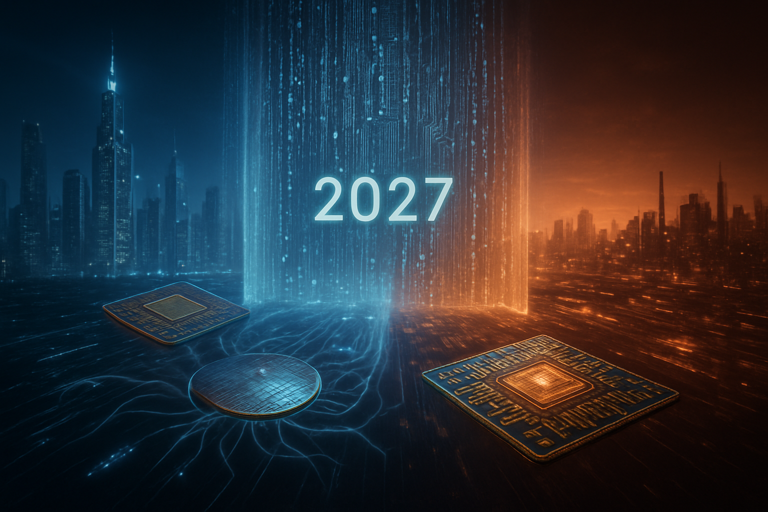
On December 23, 2025, the Trump administration fundamentally altered the trajectory of the global technology sector by announcing a strategic delay on new tariffs for Chinese-made semiconductors. While the administration’s Section 301 investigation reaffirmed that China’s trade practices are "unreasonable" and "burdensome," the Office of the U.S. Trade Representative (USTR) has opted to set the tariff rate on legacy chips at 0% until June 23, 2027. This 18-month window provides a critical buffer for a global supply chain that remains deeply intertwined with Chinese manufacturing, even as the "Silicon Curtain" begins to descend.
The decision is a calculated pivot in the "tech Cold War," shifting the focus from the immediate denial of technology to a structured, time-bound financial deterrence. By delaying the 25-50% tariffs that were expected to go into effect in early 2026, the administration aims to prevent a massive inflationary shock to the automotive and consumer electronics sectors. For the AI industry, this reprieve offers a brief moment of stability in an era of unprecedented geopolitical volatility, allowing the West to build out its domestic "Silicon Shield" before the trade barriers become permanent.
Strategic De-escalation and the Legacy Chip Buffer
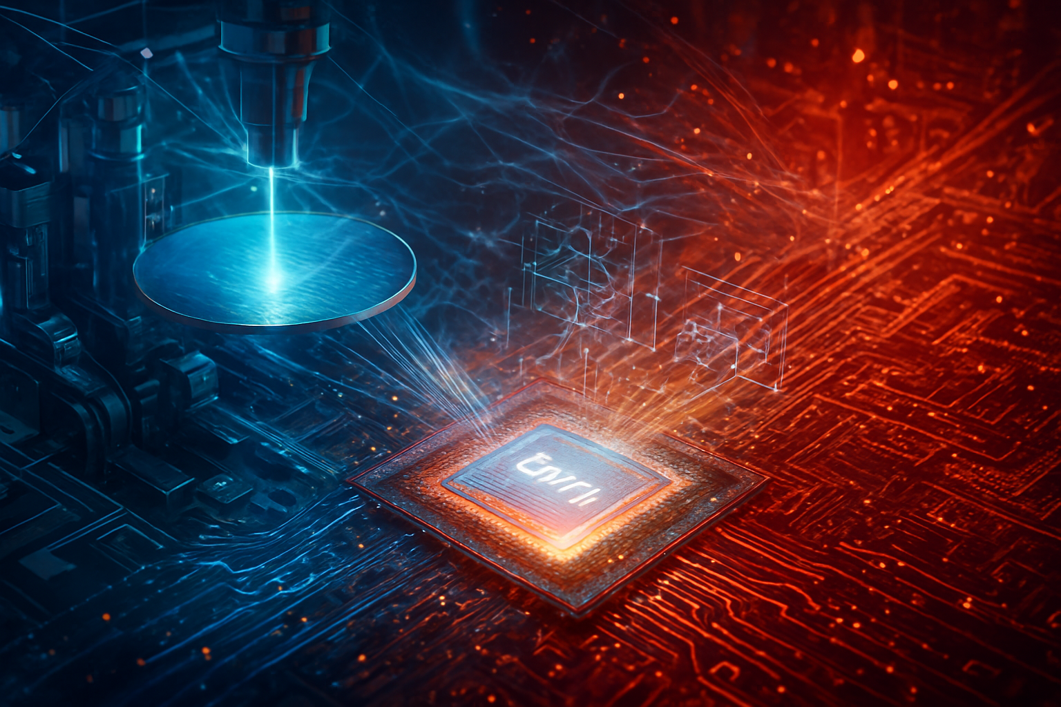
The 18-month window specifically targets "legacy" or mature-node semiconductors—typically those produced on 28nm processes or older. While these are not the cutting-edge chips used to train frontier AI models like GPT-5 or Llama 4, they are the essential "workhorses" of the modern world. These chips power everything from the power management systems in electric vehicles to the sensors in medical devices and the basic networking hardware that supports AI data centers. Immediate tariffs on these components would have likely crippled U.S. manufacturing, as domestic alternatives are not yet operating at the necessary scale.
Initial reactions from the AI research community and industry experts have been pragmatic. Economists note that the delay serves as a vital "carrot" in ongoing negotiations with Beijing, particularly regarding China’s dominance over rare earth minerals like gallium and germanium, which are essential for domestic chip production. By pushing the "tariff cliff" to mid-2027, the U.S. is betting that its multi-billion-dollar investments in domestic fabrication—led by the CHIPS Act and private capital—will be ready to absorb the demand currently met by Chinese foundries.
The Corporate Pivot: Winners and the Cost of Security
Major technology players have responded to the news with a mixture of relief and accelerated strategic shifts. NVIDIA (NASDAQ: NVDA) saw a relief rally following the announcement, as the delay ensures that the basic components required for its massive "Stargate" AI infrastructure projects remain affordable in the short term. However, the company is already preparing for the 2027 deadline by diversifying its assembly partners and pushing for more U.S.-based integration. Similarly, Apple (NASDAQ: AAPL) has utilized this window to double down on its $100 billion manufacturing commitment, with the TSMC (NYSE: TSM) Arizona fabs now serving as the centerpiece for "tariff-shielded" production of its AI-enabled A-series and M-series processors.
Intel (NASDAQ: INTC) stands to be a primary beneficiary of the 2027 cliff. As the company works to perfect its 18A process node by 2026, the looming tariffs on Chinese competitors act as a powerful incentive for domestic "hyperscalers" like Microsoft (NASDAQ: MSFT) and Alphabet (NASDAQ: GOOGL) to migrate their hardware orders to Intel’s domestic foundries. For these tech giants, the 18-month reprieve is not a return to the status quo, but a final warning to "reshore" their supply chains or face a projected 15-25% increase in AI server costs once the tariffs are fully implemented.
From Export Controls to Economic Statecraft
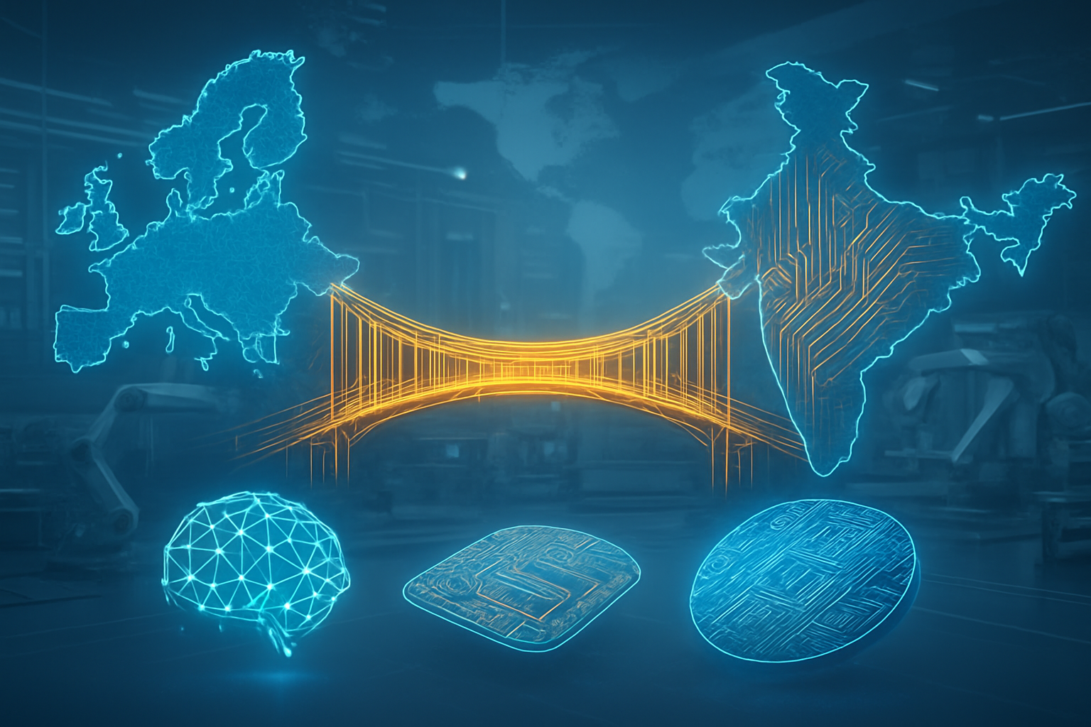
The emergence of the "Silicon Curtain" marks a transition from the 2022-era export controls to a new regime of economic statecraft. While the 2022 policies focused on denying China access to high-end AI accelerators, the 2027 tariff plan uses cost as a weapon to force a geographical shift in manufacturing. This creates a "bifurcation" of the global tech stack, where the world is split into two incompatible ecosystems: one led by the U.S. and its allies, focused on high-performance, market-driven AI, and another led by China, focused on state-subsidized "sovereign" silicon.
This shift carries a potential "Innovation Tax." Analysts warn that the rising cost of secure, non-Chinese hardware could raise the total cost of building cutting-edge AI data centers by nearly 17%. Such a barrier may consolidate power within the "Trillion-Dollar Club"—including Meta (NASDAQ: META) and Amazon (NASDAQ: AMZN)—while pricing out smaller AI startups and academic labs. Furthermore, there is a growing concern that this fragmentation will hinder global AI safety efforts, as the two technological blocs may develop diverging standards for alignment and governance.
The Horizon: 2027 and the Rise of Edge AI
Looking ahead, the industry is preparing for a "structural cliff" in June 2027. To mitigate the high costs of centralized, tariff-impacted data centers, many experts predict a surge in "Edge AI" and software optimization. By making models "lighter" through techniques like quantization, companies may be able to run sophisticated AI applications on older, more affordable legacy chips that are currently exempt from the most aggressive trade restrictions. We are also likely to see the rise of "Sovereign AI" hubs in neutral regions like the UAE or Japan, which could become attractive destinations for training frontier models outside the immediate blast radius of the US-China trade war.
The immediate challenge remains the "reshoring" timeline. If the TSMC Arizona sites and Intel’s Ohio expansions face further delays or yield issues, the 2027 deadline could lead to aggressive stockpiling and market volatility in late 2026. The administration has signaled that the 18-month window is firm, but the tech industry’s ability to reinvent its supply chain in such a short period will be the ultimate test of the "Silicon Shield" theory.
A New Chapter in Technological Sovereignty
The Trump administration’s decision to delay semiconductor tariffs until 2027 is a defining moment in the history of the AI age. It acknowledges the reality of global interdependence while simultaneously signaling its end. By creating this 18-month buffer, the U.S. has granted the tech industry a final opportunity to decouple from Chinese manufacturing without triggering a global recession.
As we move into 2026, the industry must watch for the completion of domestic fabs and the potential for China to retaliate via further export restrictions on critical minerals. The "Silicon Curtain" is no longer a theoretical concept—it is a policy reality. The next 18 months will determine whether the West can successfully build a self-sustaining AI infrastructure or if the 2027 tariff cliff will lead to a period of prolonged technological inflation and fragmented innovation.
This content is intended for informational purposes only and represents analysis of current AI developments.
TokenRing AI delivers enterprise-grade solutions for multi-agent AI workflow orchestration, AI-powered development tools, and seamless remote collaboration platforms.
For more information, visit https://www.tokenring.ai/.