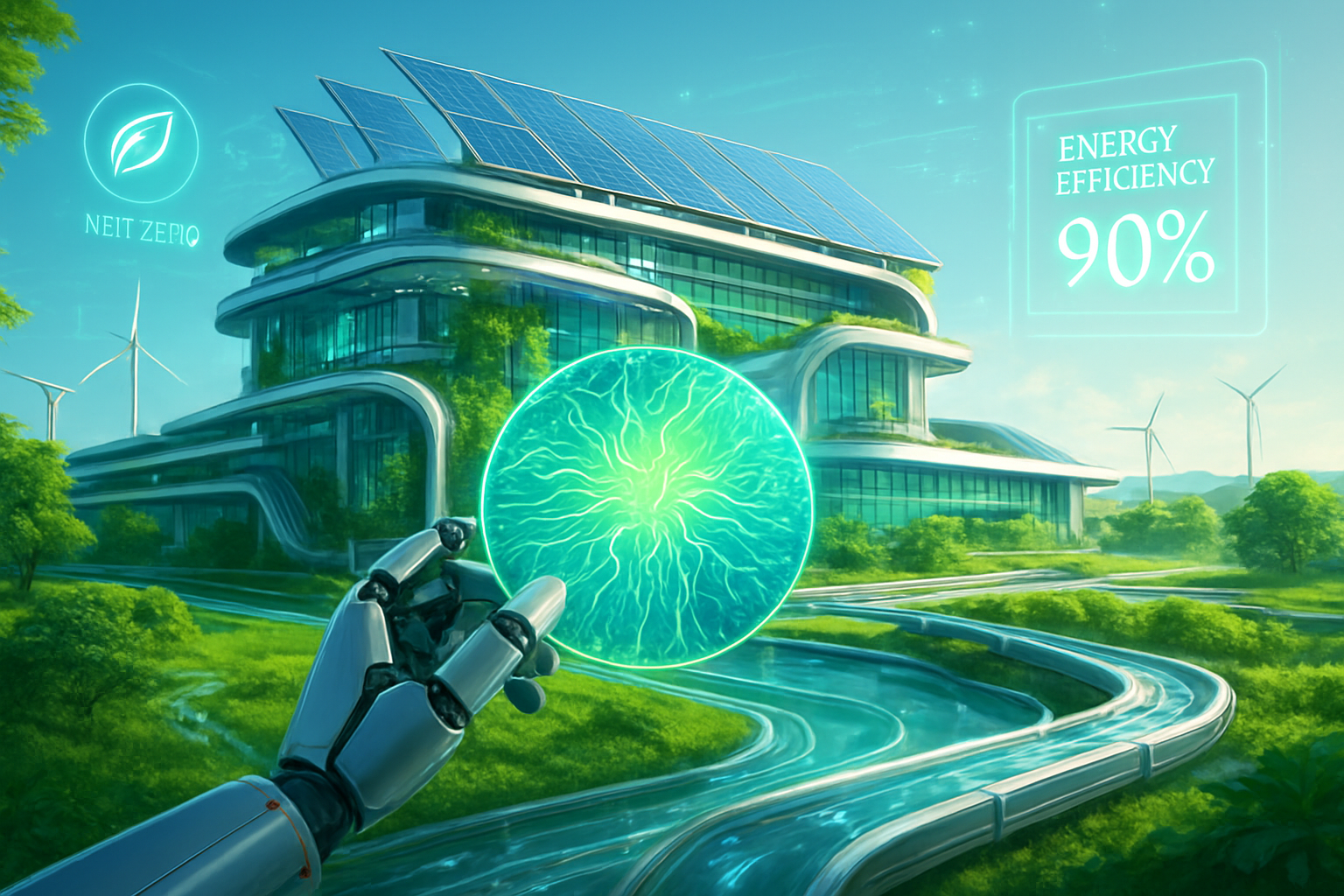
Tag: Sustainability

  • OpenAI and Hitachi Forge Alliance to Power the Future of AI with Sustainable Infrastructure

    OpenAI and Hitachi Forge Alliance to Power the Future of AI with Sustainable Infrastructure

    In a landmark strategic cooperation agreement, OpenAI and Japanese industrial giant Hitachi (TSE: 6501) have joined forces to tackle one of the most pressing challenges facing the burgeoning artificial intelligence industry: the immense power and cooling demands of AI data centers. Announced around October 2nd or 3rd, 2025, this partnership is set to develop and implement advanced, energy-efficient solutions crucial for scaling OpenAI's generative AI models and supporting its ambitious global infrastructure expansion, including the multi-billion dollar "Stargate" project.

    The immediate significance of this collaboration cannot be overstated. As generative AI models continue to grow in complexity and capability, their computational requirements translate directly into unprecedented energy consumption and heat generation. This alliance directly addresses these escalating demands, aiming to overcome a critical bottleneck in the sustainable growth and widespread deployment of AI technologies. By combining OpenAI's cutting-edge AI advancements with Hitachi's deep industrial expertise in energy, power grids, and cooling, the partnership signals a crucial step towards building a more robust, efficient, and environmentally responsible foundation for the future of artificial intelligence.

    Technical Foundations for a New Era of AI Infrastructure

    The strategic cooperation agreement between OpenAI and Hitachi (TSE: 6501) is rooted in addressing the fundamental physical constraints of advanced AI. Hitachi's contributions are centered on supplying essential infrastructure for OpenAI's rapidly expanding data centers. This includes providing robust power transmission and distribution equipment, such as high-efficiency transformers, vital for managing the colossal and often fluctuating electricity loads of AI workloads. Crucially, Hitachi will also deploy its advanced air conditioning and cooling technologies. While specific blueprints are still emerging, it is highly anticipated that these solutions will heavily feature liquid cooling methods, such as direct-to-chip or immersion cooling, building upon Hitachi's existing portfolio of pure water cooling systems.

    These envisioned solutions represent a significant departure from traditional data center paradigms. Current data centers predominantly rely on air cooling, a method that is becoming increasingly insufficient for the extreme power densities generated by modern AI hardware. AI server racks, projected to reach 50 kW or even 100 kW by 2027, generate heat that air cooling struggles to dissipate efficiently. Liquid cooling, by contrast, can remove heat directly from components like Graphics Processing Units (GPUs) and Central Processing Units (CPUs), offering up to a 30% reduction in energy consumption for cooling, improved performance, and a smaller physical footprint for high-density environments. Furthermore, the partnership emphasizes the integration of renewable energy sources and smart grid technologies, moving beyond conventional fossil fuel reliance to mitigate the substantial carbon footprint of AI. Hitachi's Lumada digital platform will also play a role, with OpenAI's large language models (LLMs) potentially being integrated to optimize energy usage and data center operations through AI-driven predictive analytics and real-time monitoring.

    The necessity for such advanced infrastructure stems directly from the extraordinary computational demands of modern AI, particularly large language models (LLMs). Training and operating these models require immense amounts of electricity; a single large AI model can consume energy equivalent to 120 U.S. homes in a year. For instance, OpenAI's GPT-3 consumed an estimated 284,000 kWh during training, with subsequent models like GPT-4 being even more power-hungry. This intense processing generates substantial heat, which, if not managed, can lead to hardware degradation and system failures. Beyond power and cooling, LLMs demand vast memory and storage, often exceeding single accelerator capacities, and require high-bandwidth, low-latency networks for distributed processing. The ability to scale these resources reliably and efficiently is paramount, making robust power and cooling solutions the bedrock of future AI innovation.

    Reshaping the AI Competitive Landscape

    The strategic alliance between OpenAI and Hitachi (TSE: 6501) is set to send ripples across the AI industry, impacting tech giants, specialized AI labs, and startups alike. OpenAI, at the forefront of generative AI, stands to gain immensely from Hitachi's deep expertise in industrial infrastructure, securing the stable, energy-efficient data center foundations critical for scaling its operations and realizing ambitious projects like "Stargate." This partnership also provides a significant channel for OpenAI to deploy its LLMs into high-value, real-world industrial applications through Hitachi's well-established Lumada platform.

    Hitachi, in turn, gains direct access to OpenAI's cutting-edge generative AI models, which will significantly enhance its Lumada digital transformation support business across sectors like energy, mobility, and manufacturing. This strengthens Hitachi's position as a provider of advanced, AI-driven industrial and social infrastructure solutions. Indirectly, Microsoft (NASDAQ: MSFT), a major investor in OpenAI and a strategic partner of Hitachi, also benefits. Hitachi's broader commitment to integrating OpenAI's technology, often via Azure OpenAI Service, reinforces Microsoft's ecosystem and its strategic advantage in providing enterprise-grade AI cloud services. Companies specializing in industrial IoT, smart infrastructure, and green AI technologies are also poised to benefit from the intensified focus on energy efficiency and AI integration.

    The competitive implications for major AI labs like Google DeepMind (NASDAQ: GOOGL), Anthropic, and Meta AI (NASDAQ: META) are substantial. This partnership solidifies OpenAI's enterprise market penetration, particularly in industrial sectors, intensifying the race for enterprise AI adoption. It also underscores a trend towards consolidation around major generative AI platforms, making it challenging for smaller LLM providers to gain traction without aligning with established tech or industrial players. The necessity of combining advanced AI models with robust, energy-efficient infrastructure highlights a shift towards "full-stack" AI solutions, where companies offering both software and hardware/infrastructure capabilities will hold a significant competitive edge. This could disrupt traditional data center energy solution providers, driving rapid innovation towards more sustainable and efficient technologies. Furthermore, integrating LLMs into industrial platforms like Lumada is poised to create a new generation of intelligent industrial applications, potentially disrupting existing industrial software and automation systems that lack advanced generative AI capabilities.

    A Broader Vision for Sustainable AI

    The OpenAI-Hitachi (TSE: 6501) agreement is more than just a business deal; it's a pivotal moment reflecting critical trends in the broader AI landscape. It underscores the global race to build massive AI data centers, a race where the sheer scale of computational demand necessitates unprecedented levels of investment and multi-company collaboration. As part of OpenAI's estimated $500 billion "Stargate" project, which involves other major players like SoftBank Group (TYO: 9984), Oracle (NYSE: ORCL), NVIDIA (NASDAQ: NVDA), Samsung (KRX: 005930), and SK Hynix (KRX: 000660), this partnership signals that the future of AI infrastructure requires a collective, planetary-scale effort.

    Its impact on AI scalability is profound. By ensuring a stable and energy-efficient power supply and advanced cooling, Hitachi directly alleviates bottlenecks that could otherwise hinder the expansion of OpenAI's computing capacity. This allows for the training of larger, more complex models and broader deployment to a growing user base, accelerating the pursuit of Artificial General Intelligence (AGI). This focus on "greener AI" is particularly critical given the environmental concerns surrounding AI's exponential growth. Data centers, even before the generative AI boom, contributed significantly to global greenhouse gas emissions, with a single model like GPT-3 having a daily carbon footprint equivalent to several tons of CO2. The partnership's emphasis on energy-saving technologies and renewable energy integration is a proactive step to mitigate these environmental impacts, making sustainability a core design principle for next-generation AI infrastructure.

    Comparing this to previous AI milestones reveals a significant evolution. Early AI relied on rudimentary mainframes, followed by the GPU revolution and cloud computing, which primarily focused on maximizing raw computational throughput. The OpenAI-Hitachi agreement marks a new phase, moving beyond just raw power to a holistic view of AI infrastructure. It's not merely about building bigger data centers, but about building smarter, more sustainable, and more resilient ones. This collaboration acknowledges that specialized industrial expertise in energy management and cooling is as vital as chip design or software algorithms. It directly addresses the imminent energy bottleneck, distinguishing itself from past breakthroughs by focusing on how to power that processing sustainably and at an immense scale, thereby positioning itself as a crucial development in the maturation of AI infrastructure.

    The Horizon: Smart Grids, Physical AI, and Unprecedented Scale

    The OpenAI-Hitachi (TSE: 6501) partnership sets the stage for significant near-term and long-term developments in AI data center infrastructure and industrial applications. In the near term, the immediate focus will be on the deployment of Hitachi's advanced cooling and power distribution systems to enhance the energy efficiency and stability of OpenAI's data centers. Simultaneously, the integration of OpenAI's LLMs into Hitachi's Lumada platform will accelerate, yielding early applications in industrial digital transformation.

    Looking ahead, the long-term impact involves a deeper integration of energy-saving technologies across global AI infrastructure, with Hitachi potentially expanding its role to other critical data center components. This collaboration is a cornerstone of OpenAI's "Stargate" project, hinting at a future where AI data centers are not just massive but also meticulously optimized for sustainability. The synergy will unlock a wide array of applications: from enhanced AI model development with reduced operational costs for OpenAI, to secure communication, optimized workflows, predictive maintenance in sectors like rail, and accelerated software development within Hitachi's Lumada ecosystem. Furthermore, Hitachi's parallel partnership with NVIDIA (NASDAQ: NVDA) to build a "Global AI Factory" for "Physical AI"—AI systems that intelligently interact with and optimize the real world—will likely see OpenAI's models integrated into digital twin simulations and autonomous industrial systems.

    Despite the immense potential, significant challenges remain. The extreme power density and heat generation of AI hardware are straining utility grids and demanding a rapid, widespread adoption of advanced liquid cooling technologies. Scaling AI infrastructure requires colossal capital investment, along with addressing supply chain vulnerabilities and critical workforce shortages in data center operations. Experts predict a transformative period, with the AI data center market projected to grow at a 28.3% CAGR through 2030, and one-third of global data center capacity expected to be dedicated to AI by 2025. This will necessitate widespread liquid cooling, sustainability-driven innovation leveraging AI itself for efficiency, and a trend towards decentralized and on-site power generation to manage fluctuating AI loads. The OpenAI-Hitachi partnership exemplifies this future: a collaborative effort to build a resilient, efficient, and sustainable foundation for AI at an unprecedented scale.

    A New Blueprint for AI's Future

    The strategic cooperation agreement between OpenAI and Hitachi (TSE: 6501) represents a pivotal moment in the evolution of artificial intelligence, underscoring a critical shift in how the industry approaches its foundational infrastructure. This partnership is a clear acknowledgment that the future of advanced AI, with its insatiable demand for computational power, is inextricably linked to robust, energy-efficient, and sustainable physical infrastructure.

    The key takeaways are clear: Hitachi will provide essential power and cooling solutions to OpenAI's data centers, directly addressing the escalating energy consumption and heat generation of generative AI. In return, OpenAI's large language models will enhance Hitachi's Lumada platform, driving industrial digital transformation. This collaboration, announced around October 2nd or 3rd, 2025, is a crucial component of OpenAI's ambitious "Stargate" project, signaling a global race to build next-generation AI infrastructure with sustainability at its core.

    In the annals of AI history, this agreement stands out not just for its scale but for its integrated approach. Unlike previous milestones that focused solely on algorithmic breakthroughs or raw computational power, this partnership champions a holistic vision where specialized industrial expertise in energy management and cooling is as vital as the AI models themselves. It sets a new precedent for tackling AI's environmental footprint proactively, potentially serving as a blueprint for future collaborations between AI innovators and industrial giants worldwide.

    The long-term impact could be transformative, leading to a new era of "greener AI" and accelerating the penetration of generative AI into traditional industrial sectors. As AI continues its rapid ascent, the OpenAI-Hitachi alliance offers a compelling model for sustainable growth and a powerful synergy between cutting-edge digital intelligence and robust physical infrastructure. In the coming weeks and months, industry observers should watch for detailed project rollouts, performance metrics on energy efficiency, new Lumada integrations leveraging OpenAI's LLMs, and any further developments surrounding the broader "Stargate" initiative, all of which will provide crucial insights into the unfolding future of AI.

    This content is intended for informational purposes only and represents analysis of current AI developments.

    TokenRing AI delivers enterprise-grade solutions for multi-agent AI workflow orchestration, AI-powered development tools, and seamless remote collaboration platforms.
    For more information, visit https://www.tokenring.ai/.

  • The Green Revolution in Silicon: Semiconductor Industry Forges a Sustainable Future

    The Green Revolution in Silicon: Semiconductor Industry Forges a Sustainable Future

    The semiconductor industry, the foundational bedrock of our digital world, is embarking on a profound transformation to reconcile its immense technological contributions with its significant environmental footprint. As the global demand for advanced chips—especially those powering the burgeoning field of Artificial Intelligence—continues its exponential ascent, the urgency for sustainable manufacturing practices has reached a critical inflection point. This shift is not merely a regulatory compliance exercise but a strategic imperative, driven by escalating energy demands, mounting environmental scrutiny, and a commitment to reducing the industry's overall ecological impact.

    This green revolution in silicon manufacturing signifies a concerted effort to integrate energy efficiency, reduce environmental harm, and implement cutting-edge green technologies across every stage of chip production. From sourcing raw materials to the intricate fabrication processes within multi-billion-dollar fabs, companies are redefining what it means to produce the brains of modern technology responsibly. This immediate and impactful pivot is crucial for ecological preservation and vital for the industry's economic resilience, regulatory adherence, and continued innovation in an increasingly environmentally conscious global technology landscape.

    Engineering a Greener Chip: Technical Advancements and Eco-Conscious Production

    The pursuit of sustainability in semiconductor manufacturing is catalyzing a wave of groundbreaking technical advancements and the widespread adoption of green technologies, marking a significant departure from older, more resource-intensive production methods. At the heart of this transformation are innovations aimed at drastically reducing energy consumption, conserving water, minimizing chemical waste, and abating greenhouse gas emissions.

    A primary focus is renewable energy integration and overall energy efficiency. Fabrication plants (fabs) are aggressively transitioning to powering their operations with renewable sources like solar and wind. Companies like Intel (NASDAQ: INTC) have committed to 100% renewable electricity across their global operations by 2030, while Taiwan Semiconductor Manufacturing Company (NYSE: TSM) has advanced its RE100 goal to 2040. Beyond sourcing, "green fabs" are being designed with optimized infrastructure, advanced HVAC systems, and energy-efficient equipment. Process-level efficiencies are also critical, with advancements like Extreme Ultraviolet (EUV) lithography being optimized to reduce energy per wafer. Notably, TSMC's "EUV Dynamic Energy Saving Program," launched in September 2025, has already demonstrated a 44% reduction in peak power consumption of EUV tools, projected to save 190 million kilowatt-hours (kWh) of electricity and cut carbon emissions by 101 kilotons by 2030. Furthermore, the adoption of advanced materials like Gallium Nitride (GaN) and Silicon Carbide (SiC) offers superior energy efficiency in power electronics compared to traditional silicon. AI and machine learning (ML) are also being deployed to optimize manufacturing processes, enabling precise control over resource usage and reducing energy consumption by up to 30% in idle tools.

    Water reclamation and conservation represent another critical area of innovation. Semiconductor fabs require immense volumes of ultrapure water, making water scarcity a growing concern. Manufacturers are implementing sophisticated multi-stage recycling systems, including advanced Reverse Osmosis (RO) filtration and electro-deionization (EDI), to treat and reuse process water, achieving high recycling rates. For instance, GlobalFoundries has announced a breakthrough wastewater treatment technology achieving a 98% recycling rate. Intel, for its part, restored over 2 billion gallons of water to local communities in 2022 and aims for net-positive water by 2030. These closed-loop systems and optimization efforts contrast sharply with older methods that often involved significant fresh water intake and less efficient wastewater management.

    In terms of green chemistry and emissions reduction, the industry is tackling the challenge of fluorinated gases (F-GHGs), potent greenhouse gases used in etching and chamber cleaning. Strategies include optimizing production processes, switching to alternative input gases, and installing advanced abatement systems to detoxify exhaust gases. Samsung (KRX: 005930) developed a Regenerative Catalytic System (RCS) that achieves up to 95% processing efficiency for greenhouse gas emissions. Companies are also moving towards substituting hazardous chemicals with more environmentally friendly alternatives. The shift from older methods, which often released a significant percentage of unreacted gases into the atmosphere, to these precise control and abatement systems is a substantial leap forward. Finally, waste reduction and circular economy principles are gaining traction, with efforts in silicon and chemical recycling, sustainable packaging, and promoting product life extension to minimize electronic waste. Lam Research (NASDAQ: LRCX), for example, has introduced technologies like Lam Cryo™ 3.0, which delivers a projected 40% reduction in energy consumption per wafer and cuts process gas emissions by approximately 90%, and utilizes virtual twin technology to reduce emissions by up to 80% by replacing physical experimentation with digital simulation. These integrated sustainability approaches contrast with past practices where environmental concerns were often an afterthought, showcasing a fundamental re-engineering of the entire manufacturing ethos.

    Reshaping the Tech Landscape: Industry Impact and Competitive Dynamics

    The accelerating drive towards sustainability in semiconductor manufacturing is sending ripples across the entire tech industry, fundamentally altering competitive landscapes, influencing product development, and creating new strategic advantages for companies ranging from AI innovators to established tech giants and agile startups.

    Tech giants such as Apple (NASDAQ: AAPL), Google (NASDAQ: GOOGL), Microsoft (NASDAQ: MSFT), and Amazon (NASDAQ: AMZN) are at the forefront of demanding more sustainable practices from their semiconductor suppliers. Many have committed to ambitious net-zero emissions goals, with deadlines approaching (e.g., Apple aiming for carbon-neutral silicon production by 2030). This translates into rigorous supply chain requirements, pushing chipmakers to accelerate their green initiatives. Companies that can deliver energy-efficient, sustainably produced chips stand to benefit immensely, securing lucrative contracts and strengthening partnerships with these influential buyers. This competitive pressure encourages major semiconductor manufacturers like TSMC, Intel, and Samsung to invest heavily in sustainable fabs and processes, positioning them as leaders and attracting environmentally conscious customers.

    For AI companies, the relationship with semiconductor sustainability is dual-edged. The explosive growth of AI fuels an insatiable demand for computational power, leading to a surge in energy consumption, particularly in data centers. TechInsights forecasts a staggering 300% increase in CO2 emissions from AI accelerators alone between 2025 and 2029, highlighting the urgent need for sustainable solutions. This puts pressure on AI firms to prioritize energy-efficient chip designs and optimize data center operations. Conversely, AI itself is emerging as a powerful tool for achieving sustainability in semiconductor manufacturing, optimizing processes, reducing waste, and enabling predictive maintenance. Companies that leverage AI for sustainable design and manufacturing, alongside developing inherently energy-efficient AI chips (e.g., Google's TPUs), will gain a significant competitive edge by reducing operational costs and appealing to a growing segment of environmentally aware customers and investors.

    Startups, while facing high barriers to entry in the semiconductor space, are finding vast opportunities in niche areas of sustainable innovation. Initiatives like "Startups for Sustainable Semiconductors (S3)" are connecting climate tech startups with corporate venture capitalists, fostering innovation in areas such as advanced cooling technologies, sustainable materials, chemical recovery, PFAS destruction, and AI-driven energy management. These agile innovators can disrupt existing products and services by offering greener alternatives for production processes, energy-efficient equipment, or materials with lower environmental impact. The shift towards circular design principles—products designed for reuse, repair, and easier material recovery—will also challenge traditional "take-make-dispose" models, favoring companies that embrace product longevity and resource efficiency. Overall, sustainability is no longer just a compliance issue; it's a strategic differentiator that will redefine market positioning and reward companies that proactively integrate environmental responsibility into their core business models.

    AI's Green Imperative: Broader Significance and Evolving Landscape

    The drive for sustainability in semiconductor manufacturing holds profound wider significance, particularly as it intersects with the burgeoning Artificial Intelligence landscape. This convergence highlights both the environmental challenges posed by AI's rapid expansion and the critical role of sustainable chip production in mitigating these impacts, shaping the future trajectory of technology itself.

    The semiconductor industry’s environmental footprint is substantial. In 2020, the sector emitted approximately 64.24 million tons of CO2-equivalent gases, with energy consumption in fabs comparable to small cities. The demand for ultrapure water runs into millions of gallons daily, and the use of hazardous chemicals like perfluorocarbons (PFCs), potent greenhouse gases, contributes significantly to pollution. The "AI Gold Rush" exacerbates these issues, as AI's "insatiable hunger" for computational power directly translates into increased demand for chips, further straining resources. Data centers, the backbone of AI, are projected to triple their power consumption by 2030, with AI workloads consuming 10 to 30 times more electricity than traditional computing tasks. This unprecedented scale of demand, projected to push the global semiconductor market to $800 billion in 2025, positions semiconductor sustainability as a paramount concern for the entire digital ecosystem.

    However, this heightened environmental awareness also presents potential concerns. The high cost of transitioning to greener production processes, involving substantial initial capital investments, can be an obstacle. The sheer complexity of chip production, with over 300 individual steps, makes it challenging for outside innovators to introduce sustainable solutions. Regulatory conflicts, such as restrictions on certain chemicals (e.g., PFAS bans) used in manufacturing, can create tension between economic security and sustainability objectives. Despite these challenges, the current focus on sustainability represents a significant evolution from previous tech milestones. While past technological advancements also increased energy consumption, the current urgency is driven by a global climate crisis, with policymakers and customers now prioritizing ecological concerns alongside supply security—a marked shift from earlier eras where environmental impact was often an afterthought.

    This push for green manufacturing aligns with broader AI trends, where the technology itself is becoming a solution to the very problems it exacerbates. AI and Machine Learning are pivotal in optimizing resource usage, designing energy-efficient chips, and streamlining manufacturing processes. This dual nature—AI as both a driver of demand and a tool for sustainability—underscores its critical role in shaping a more responsible technological future. The industry is actively pursuing solutions such as green hydrogen adoption, advanced water reclamation systems, eco-friendly material usage, and circular economy practices, all of which are increasingly informed and optimized by AI. This integrated approach, where sustainability is embedded into core design and operational philosophies, marks a new era for technology development, demanding a balance between innovation and environmental responsibility.

    The Horizon of Green Silicon: Future Developments and Expert Outlook

    The journey towards a fully sustainable semiconductor industry is a long-term endeavor, but the trajectory of future developments points towards a deeply integrated and technologically advanced approach to environmental stewardship. Both near-term and long-term trends indicate a profound reshaping of how chips are designed, manufactured, and utilized.

    In the near term (1-5 years), the industry will see an accelerated integration of renewable energy, with major chipmakers like Intel (NASDAQ: INTC) targeting 100% renewable electricity by 2030, and TSMC (NYSE: TSM) aiming for 25% from renewable sources by the same year. Water conservation will remain a critical focus, with advanced reclamation systems becoming standard, potentially mandated by stricter regulations such as those proposed by the European Union. Expect to see continued emphasis on sustainable material sourcing and the adoption of "green chemistry," replacing hazardous chemicals and optimizing gas usage. Efforts to reduce "Scope 3" emissions—indirect emissions from the supply chain—will also intensify as companies seek to holistically address their environmental footprint.

    Looking further into the long term (5-10+ years), the industry is poised for more transformative changes to achieve ambitious net-zero and carbon-neutral goals by 2050. This will involve significant R&D into novel, sustainable materials beyond traditional silicon, such as organic semiconductors and perovskites, to enable even more energy-efficient AI. Wide-bandgap materials like Gallium Nitride (GaN) and Silicon Carbide (SiC) will become more prevalent, especially in power electronics for electric vehicles and renewable energy systems. The full realization of circular economy principles will see chips designed for disassembly, and advanced recycling methods for critical raw material recovery will become standard practice. Experts predict the increasing integration of green hydrogen for fabrication processes and the potential for nuclear-powered systems to meet the immense energy demands of future AI-driven fabs. Smart manufacturing, leveraging end-to-end digitalization, AI, and machine learning, will be crucial for optimizing every aspect of production, from energy and water consumption to yield and quality control.

    The potential applications of these sustainable semiconductor advancements are vast. They will be integral to electric vehicles (EVs), enhancing efficiency in charging and motor control. They will power more efficient renewable energy systems (solar cells, smart grids) and drastically reduce energy consumption in data centers and cloud computing. Crucially, innovations like organic semiconductors promise significantly lower power consumption for AI accelerators and edge computing devices, enabling more distributed and sustainable AI deployments. However, significant challenges persist, including the high energy consumption of advanced nodes, massive water usage, the continued reliance on hazardous chemicals, and the growing volume of e-waste. The complexity of global supply chains also makes it difficult to track and reduce Scope 3 emissions effectively. Experts like Michael Luciano from Jama Software anticipate continued research into novel materials and refined processes, with AI playing a pivotal role in optimizing designs, modeling energy consumption, and managing resources in real-time. The future hinges on a collaborative, innovative, and adaptive approach, balancing technological advancement with environmental responsibility.

    The Dawn of Sustainable AI: A Comprehensive Wrap-Up

    The semiconductor industry stands at a critical juncture, where the relentless march of technological innovation, particularly in Artificial Intelligence, must be harmonized with an unwavering commitment to environmental stewardship. This comprehensive review underscores that sustainability in semiconductor manufacturing is not a peripheral concern but a foundational imperative, reshaping the very essence of how our digital future is built.

    The key takeaways are clear: the semiconductor sector, while indispensable, is inherently resource-intensive, demanding vast quantities of energy, water, and chemicals, leading to significant greenhouse gas emissions. The exponential growth of AI exacerbates these environmental challenges, with AI accelerators alone projected to cause a 300% increase in CO2 emissions between 2025 and 2029. However, the industry is responding with a robust "green revolution," driven by increasing climate awareness, stringent regulations, investor demands, and the economic benefits of efficiency. Leading companies are making ambitious commitments to net-zero emissions and 100% renewable energy, underpinned by innovations in advanced water reclamation, circular economy practices, green chemistry, energy-efficient chip design, and the transformative power of AI and machine learning in optimizing every aspect of production.

    The significance of this development in AI history is profound and dual-faceted. On one hand, AI's insatiable hunger for computational power presents a formidable environmental challenge, extending its carbon footprint from operational phases to its very genesis in semiconductor fabs. Without "greener silicon," the full transformative promise of AI could be overshadowed by its escalating ecological cost. Conversely, AI itself is emerging as an indispensable tool for achieving sustainability within semiconductor manufacturing, enabling precise control, optimizing resource utilization, and driving the design of more efficient processes. This symbiotic relationship underscores that sustainable chip production is not merely an ethical consideration but a foundational requirement for the long-term viability and ethical development of AI itself.

    Looking at the long-term impact, sustainability is transcending its role as mere compliance, evolving into a primary driver of innovation, competitiveness, and new revenue streams. Green manufacturing practices are expected to significantly reduce operational costs, bolstering economic viability. Achieving these ambitious goals will necessitate unprecedented global collaboration across the entire value chain, fostering a more circular economy model where design for longevity, repairability, and material reuse becomes standard. Further research into novel, sustainable materials beyond silicon, such as organic semiconductors and wide-bandgap materials, will enable even more energy-efficient AI and power electronics.

    What to watch for in the coming weeks and months includes the formal details and funding allocations from initiatives like the CHIPS for America program, alongside new legislation such as the EU's proposed stricter water usage regulations for semiconductor fabs. Keep an eye on accelerated corporate sustainability commitments from top semiconductor companies, particularly regarding net-zero targets and renewable energy adoption. Monitor technological breakthroughs in green hydrogen integration, advanced water recycling, and the development of new eco-friendly materials. Crucially, observe the expanding role of AI and machine learning in optimizing manufacturing processes and designing more energy-efficient chips, while simultaneously tracking the energy consumption trends of AI accelerators to gauge the effectiveness of mitigation strategies. Progress in industry-wide standardization efforts and increased supply chain transparency will also be key indicators of the industry's commitment to a truly sustainable future. The dawn of sustainable AI is upon us, and its evolution will be one of the most compelling narratives of the coming decades.

    This content is intended for informational purposes only and represents analysis of current AI developments.

    TokenRing AI delivers enterprise-grade solutions for multi-agent AI workflow orchestration, AI-powered development tools, and seamless remote collaboration platforms.
    For more information, visit https://www.tokenring.ai/.

  • The Green Revolution in Silicon: How Sustainable Manufacturing is Reshaping the Semiconductor Industry for the AI Era

    The Green Revolution in Silicon: How Sustainable Manufacturing is Reshaping the Semiconductor Industry for the AI Era

    The relentless march of artificial intelligence (AI) is pushing the boundaries of computational power, demanding ever more sophisticated semiconductors. Yet, this technological acceleration comes with a profound environmental cost. The semiconductor industry, a foundational pillar of the digital age, is now at a critical inflection point, grappling with its substantial ecological footprint. A burgeoning movement towards sustainability and green initiatives is rapidly transforming the entire semiconductor production process, from raw material sourcing to manufacturing and waste management. This shift is not merely an ethical choice but a strategic imperative, driven by escalating regulatory pressures, growing consumer demand for eco-conscious products, and the inherent economic benefits of resource efficiency. The immediate significance of these green endeavors is clear: to mitigate the industry's massive energy and water consumption, reduce greenhouse gas (GHG) emissions, and minimize hazardous waste, ensuring that the very building blocks of AI are forged responsibly.

    This comprehensive embrace of sustainable practices is poised to redefine the future of technology, intertwining environmental stewardship with technological advancement. As the world races to unlock AI's full potential, the industry's commitment to greener manufacturing processes is becoming paramount, addressing pressing climate concerns while simultaneously fostering innovation and enhancing long-term resilience.

    Engineering a Greener Chip: Technical Innovations Driving Sustainable Production

    Historically, semiconductor manufacturing has been a resource-intensive behemoth, characterized by immense energy consumption, prodigious water use, and the generation of hazardous waste and potent greenhouse gases. Today, a paradigm shift is underway, propelled by technical innovations that fundamentally alter how chips are made. These modern approaches represent a radical departure from older, less sustainable methodologies.

    One of the most critical areas of transformation is advanced water recycling. Semiconductor fabrication demands vast quantities of ultrapure water (UPW) for cleaning and rinsing wafers. A single 200-mm wafer can consume over 5,600 liters of water, with large fabs using up to 10 million gallons daily. Modern green initiatives employ sophisticated multi-stage recycling systems, including advanced Reverse Osmosis (RO) filtration, Ultra-filtration (UF), and electro-deionization (EDI), which can reduce chemical usage by over 95% compared to conventional ion exchange. Treated wastewater is now often repurposed for less demanding applications like cooling towers or exhaust scrubbers, rather than simply discharged. Companies like GlobalFoundries (NASDAQ: GFS) have announced breakthroughs, achieving up to a 98% recycling rate for process water, a stark contrast to older methods that relied heavily on fresh water withdrawal and less sophisticated wastewater treatment.

    Concurrently, the industry is making significant strides in Greenhouse Gas (GHG) emission reduction. Semiconductor processes utilize high Global Warming Potential (GWP) fluorinated compounds such as perfluorocarbons (PFCs) and nitrogen trifluoride (NF3). Green strategies involve a hierarchy of actions: reduce, replace, reuse/recycle, and abate. Process optimization, such as fine-tuning chamber pressure and gas flow, can reduce GHG consumption. More importantly, there's a concerted effort to replace high-GWP gases with lower-GWP alternatives like fluorine (F2) or carbonyl fluoride (COF2) for chamber cleaning. Where replacement isn't feasible, advanced abatement technologies, particularly point-of-use (POU) plasma and catalytic systems, capture and destroy unreacted GHGs with efficiencies often exceeding 99%. This is a significant leap from older practices where a higher proportion of unreacted, high-GWP gases were simply vented, and abatement technologies were less common or less effective.

    Furthermore, renewable energy integration is reshaping the energy landscape of fabs. Historically, semiconductor manufacturing was powered predominantly by grid electricity derived from fossil fuels. Today, leading companies are aggressively transitioning to diverse renewable sources, including on-site solar, wind, and even geothermal solutions. This is complemented by advanced energy management systems, intelligent microgrids, and the application of AI and Machine Learning (ML) to optimize real-time energy consumption and predict maintenance needs. The shift to Extreme Ultraviolet (EUV) lithography also plays a role, as it eliminates many multi-patterning steps required by older Deep Ultraviolet (DUV) methods, significantly lowering energy consumption per wafer. These efforts collectively aim for net-zero emissions and 100% renewable energy targets, a stark contrast to the fossil fuel reliance of the past.

    Finally, the adoption of circular economy principles is transforming material usage and waste management. This involves eco-design for products, ensuring durability, repairability, and ease of material extraction at end-of-life. Material recovery and reuse are paramount, with innovations in remanufacturing parts, recycling silicon wafers, and recovering critical raw materials (CRMs) like gallium and precious metals from processing waste. Older methods often followed a linear "take-make-dispose" model, leading to significant waste and heavy reliance on virgin raw materials. The circular approach seeks to decouple growth from resource consumption, minimize landfill waste, and create closed-loop systems for materials, driven by customer awareness, regulatory demands, and the critical business imperative for supply security.

    Corporate Green Giants: Reshaping the Semiconductor Landscape

    The imperative for sustainable semiconductor manufacturing is not just an environmental mandate; it's a powerful force reshaping competitive dynamics and market positioning across the tech industry. Major players are not only investing heavily in green initiatives but are also leveraging them as strategic differentiators.

    Intel (NASDAQ: INTC) stands out with an ambitious holistic approach, aiming for net-zero greenhouse gas emissions across Scope 1 and 2 by 2040 and Upstream Scope 3 by 2050. The company already utilizes 99% renewable energy in its global operations and is striving for zero waste to landfill by 2030, having reached 6% by 2023. This commitment enhances its brand reputation and appeals to environmentally conscious customers and investors. Taiwan Semiconductor Manufacturing Company (TSMC) (NYSE: TSM), the world's largest dedicated independent semiconductor foundry, has committed to 100% renewable energy by 2050 and is a leader in water reclamation and recycling. Their pledge to reach net-zero emissions by 2050 sets a high bar for the industry, influencing their vast network of customers, including major AI labs and tech giants.

    Other significant players like Samsung (KRX: 005930) are focused on developing low-power chips and reducing power consumption in customer products, having achieved "Triple Standard" certification for carbon, water, and waste by Carbon Trust. NVIDIA (NASDAQ: NVDA) reported that 76% of its global production energy came from renewable sources in 2023-2024, reflecting a broader industry trend. onsemi (NASDAQ: ON), recognized as a leader in semiconductor sustainability, aims for net-zero emissions by 2040 across all scopes, with approved science-based emission reduction targets. These companies stand to benefit from enhanced market position, significant cost savings through improved operational efficiency, and reduced risks associated with tightening environmental regulations.

    The shift towards green semiconductor manufacturing presents both opportunities and disruptions for major AI labs, tech giants, and startups. The explosive growth of AI is driving a surge in energy consumption, making energy-efficient AI chips a critical demand. Tech giants like Apple (NASDAQ: AAPL), Microsoft (NASDAQ: MSFT), and Daimler (ETR: MBG) are committed to achieving net-zero supply chains by specific deadlines, creating immense pressure on semiconductor suppliers to adopt sustainable practices. This influences procurement decisions, potentially favoring green-certified manufacturers and driving demand for specialized low-power AI processing architectures from innovative startups like Green Mountain Semiconductor.

    Furthermore, the focus on supply chain resilience and sustainability is leading to geopolitical shifts. Initiatives like the U.S. CHIPS for America Act and the EU Chips Act are investing heavily in local, advanced, and energy-efficient semiconductor production. This aims to secure access to chips for AI labs and tech giants, reducing dependency on volatile external supply chains. While offering stability, it could also introduce new regional supply chain dynamics and potentially higher costs for some components. Paradoxically, AI itself is becoming a critical tool for achieving sustainability in manufacturing, with AI and ML optimizing fabrication processes and reducing waste. This creates opportunities for startups developing AI-powered solutions for green manufacturing, though high initial investment costs and the challenge of finding sustainable materials with comparable performance remain significant hurdles.

    A Greener Future for AI: Wider Significance and Global Impact

    The wider significance of green initiatives in semiconductor production within the broader AI landscape is profound and multi-layered. It addresses the critical environmental challenges posed by AI's surging demand while simultaneously fostering innovation, economic competitiveness, and geopolitical stability.

    At its core, green semiconductor manufacturing is crucial for mitigating AI's environmental footprint. The production of a single high-end GPU can generate approximately 200 kg of CO₂, equivalent to driving a gasoline car over 800 miles. Without sustainable practices, the environmental cost of AI could escalate dramatically, potentially undermining its societal benefits and global climate goals. By optimizing resource consumption, minimizing chemical waste, and lowering energy use during production, these initiatives directly combat the ecological burden of AI. Furthermore, they contribute to enhancing resource security and a circular economy by reducing reliance on scarce raw materials and promoting reuse and recycling, bolstering supply chain resilience against geopolitical risks.

    This movement also aligns closely with broader environmental movements, particularly the principles of the circular economy, which aims to design out waste and pollution, keep products and materials in use, and regenerate natural systems. This echoes calls for systemic changes beyond mere "reduction" towards "rethinking" entire product lifecycles. Compared to early AI milestones, which had minimal environmental footprints due to lower computational demands, today's AI, with its unprecedented energy and resource requirements, has brought environmental costs to the forefront. The dramatic increase in computing power required for cutting-edge AI models (doubling every 3.4 months since 2012) highlights a critical difference, making green manufacturing a direct response to this accelerated environmental toll.

    However, potential concerns persist. The "bigger is better" attitude in the AI community, focusing on increasingly large models, continues to drive a massive surge in energy consumption. Data centers, the backbone of AI, are projected to increase their electricity use significantly, with some estimates suggesting a 300% increase in CO2 emissions from AI accelerators alone between 2025 and 2029. This exacerbated energy demand from AI growth challenges even the most aggressive green manufacturing efforts. The specialized nature and rapid advancement of AI hardware also contribute to a growing e-waste and obsolescence problem. Moreover, a noted lack of transparency regarding the full environmental impact of AI development and utilization means the actual emissions are often underreported, hindering accountability.

    In a powerful paradox, AI itself is becoming a tool for green manufacturing. AI and ML can optimize product designs, model energy consumption, monitor equipment for predictive maintenance, and manage water usage in real-time, potentially reducing a fab's carbon emissions by about 15%. This dual nature—AI as both an environmental burden and a solution—contrasts with earlier technological advancements where environmental impacts were often an afterthought. The current focus on green semiconductor manufacturing for AI is a crucial step towards ensuring that the technological progress powered by AI is not achieved at an unsustainable environmental cost, but rather contributes to a more sustainable future.

    The Horizon of Green Silicon: Future Developments and Expert Outlook

    The trajectory of green semiconductor manufacturing is set for transformative change, balancing the escalating demand for advanced chips with an unwavering commitment to environmental responsibility. Both near-term and long-term developments will play a crucial role in shaping this sustainable future.

    In the near-term (1-5 years), expect accelerated integration of renewable energy sources, with major chipmakers pushing to meet substantial portions of their electricity needs from clean power by 2026. Stricter water usage regulations, particularly from regions like the European Union, will drive widespread adoption of advanced water recycling technologies, aiming for even higher recycling rates than the current breakthroughs. Increased collaboration between chipmakers and designers will focus on energy-efficient chip architectures, incorporating low-power transistors and power-gating technologies. Furthermore, green chemistry will see more widespread implementation, replacing harmful chemicals with safer alternatives, and sustainable material sourcing will become a standard practice, with companies like Intel (NASDAQ: INTC) partnering with suppliers committed to responsible mining and recycled content.

    Looking to the long-term (5-10+ years), the industry is targeting ambitious goals like net-zero greenhouse gas emissions and 100% carbon-neutral power by 2050, as set by companies such as TSMC (NYSE: TSM) and GlobalFoundries (NASDAQ: GFS). Significant research will explore new, sustainable materials beyond traditional silicon, such as organic semiconductors and perovskites, to enable even more energy-efficient AI. Wide-bandgap materials like Gallium Nitride (GaN) and Silicon Carbide (SiC) will become more prevalent in power electronics, enhancing efficiency in renewable energy systems and electric vehicles. The true realization of circular economy approaches, with chips designed for disassembly and advanced recycling methods for critical raw material recovery, will be key. Experts also predict the increasing integration of green hydrogen for fabrication processes and the potential for nuclear-powered systems to meet the immense energy demands of future AI-driven fabs.

    Potential applications for these green semiconductors are vast. They are integral to Electric Vehicles (EVs), enabling efficient power electronics for charging, motor control, and energy management. They are vital for renewable energy systems like solar cells and smart grids, maximizing energy harvest. In data centers and cloud computing, green semiconductors with low-power processors and optimized circuit designs will drastically reduce energy consumption. Furthermore, innovations like organic semiconductors promise significantly lower power consumption for AI accelerators and edge computing devices, enabling more distributed and sustainable AI deployments.

    However, significant challenges persist. The high energy consumption of semiconductor manufacturing remains a hurdle, with fabs still consuming vast amounts of electricity, often from fossil fuels. Water usage and contamination continue to strain local supplies, and the management of chemical waste and pollution from hazardous substances like hydrofluoric acid is an ongoing concern. The growing volume of e-waste and the difficulty of recovering rare metals from old components also demand continuous innovation. The complexity of the global supply chain makes tracking and reducing Scope 3 emissions (indirect emissions) particularly challenging. Experts predict that carbon emissions from semiconductor manufacturing will grow at 8.3% through 2030, reaching 277 million metric tons of CO2e, driven largely by AI. This "AI Supercycle" is creating an "energy supercycle" for data centers, necessitating significant investments in sustainable energy solutions and more energy-efficient chip designs. Paradoxically, AI and ML are seen as pivotal tools, optimizing product designs, processes, and accelerating the discovery of new sustainable materials through AI-powered autonomous experimentation (AI/AE). The future demands a relentless pursuit of both green manufacturing for AI and AI for green manufacturing.

    A Sustainable Silicon Future: Charting the Path Forward

    The semiconductor industry is undergoing a profound transformation, driven by the dual pressures of unprecedented demand, particularly from the burgeoning Artificial Intelligence (AI) sector, and an urgent imperative to address its significant environmental footprint. Green initiatives are no longer peripheral but have become strategic cornerstones, redefining how chips are designed, produced, and managed across their entire lifecycle.

    The key takeaways from this green revolution are clear: a multi-faceted approach encompassing aggressive renewable energy integration, advanced water conservation and recycling, stringent waste reduction through circular economy principles, the adoption of green chemistry and sustainable materials, and the pivotal leveraging of AI and Machine Learning for process optimization. Major players like Intel (NASDAQ: INTC), TSMC (NYSE: TSM), and Samsung (KRX: 005930) are leading the charge, setting ambitious net-zero targets and investing heavily in sustainable technologies.

    The significance of this development in AI history is dual-faceted and profound. On one hand, AI's insatiable demand for computational power and advanced chips presents an enormous environmental challenge, threatening to escalate global energy consumption and carbon emissions. On the other, AI itself is emerging as an indispensable tool for achieving sustainability in semiconductor manufacturing, optimizing everything from design to resource utilization. This symbiotic relationship underscores that sustainable chip production is not merely an ethical add-on, but a foundational requirement for the long-term viability and ethical development of AI itself. Without greener silicon, the full promise of AI could be overshadowed by its ecological cost.

    Looking ahead, the long-term impact promises a redefinition of industrial responsibility. Sustainability is evolving beyond mere compliance to become a primary driver of innovation, competitiveness, and new revenue streams. The industry is moving towards a true circular economy, ensuring that the foundational components of our digital world are produced with environmental stewardship at their core. This "green revolution" in silicon is crucial not just for the semiconductor sector but for enabling a greener future across countless other industries, from electric vehicles to renewable energy systems.

    What to watch for in the coming weeks and months will be crucial indicators of this ongoing transformation. Keep a close eye on further policy and funding developments, especially from initiatives like the U.S. CHIPS for America program, which is increasingly emphasizing AI's role in sustainable chip manufacturing. Expect more detailed progress reports from leading semiconductor companies on their net-zero targets, renewable energy adoption rates, and water recycling achievements. Look for emerging technology demonstrations, particularly in 3D integration, wide bandgap semiconductors like Gallium Nitride, and the real-time AI/ML optimization of fabrication processes. Increased supply chain transparency and collaboration, driven by the focus on reducing Scope 3 emissions, will also be a key area to monitor, alongside evolving regulatory pressures from bodies like the European Union. These developments will collectively chart the path towards a truly sustainable silicon future, ensuring that the innovations powering our world are built on an environmentally responsible foundation.

    This content is intended for informational purposes only and represents analysis of current AI developments.

    TokenRing AI delivers enterprise-grade solutions for multi-agent AI workflow orchestration, AI-powered development tools, and seamless remote collaboration platforms.
    For more information, visit https://www.tokenring.ai/.

  • Navitas and Nvidia Forge Alliance: GaN Powering the AI Revolution

    Navitas and Nvidia Forge Alliance: GaN Powering the AI Revolution

    SAN JOSE, CA – October 2, 2025 – In a landmark development that promises to reshape the landscape of artificial intelligence infrastructure, Navitas Semiconductor (NASDAQ: NVTS), a leading innovator in Gallium Nitride (GaN) and Silicon Carbide (SiC) power semiconductors, announced a strategic partnership with AI computing titan Nvidia (NASDAQ: NVDA). Unveiled on May 21, 2025, this collaboration is set to revolutionize power delivery in AI data centers, enabling the next generation of high-performance computing through advanced 800V High Voltage Direct Current (HVDC) architectures. The alliance underscores a critical shift towards more efficient, compact, and sustainable power solutions, directly addressing the escalating energy demands of modern AI workloads and laying the groundwork for exascale computing.

    The partnership sees Navitas providing its cutting-edge GaNFast™ and GeneSiC™ power semiconductors to support Nvidia's 'Kyber' rack-scale systems, designed to power future GPUs such as the Rubin Ultra. This move is not merely an incremental upgrade but a fundamental re-architecture of data center power, aiming to push server rack capacities to 1-megawatt (MW) and beyond, far surpassing the limitations of traditional 54V systems. The implications are profound, promising significant improvements in energy efficiency, reduced operational costs, and a substantial boost in the scalability and reliability of the infrastructure underpinning the global AI boom.

    The Technical Backbone: GaN, SiC, and the 800V Revolution

    The core of this AI advancement lies in the strategic deployment of wide-bandgap semiconductors—Gallium Nitride (GaN) and Silicon Carbide (SiC)—within an 800V HVDC architecture. As AI models, particularly large language models (LLMs), grow in complexity and computational appetite, the power consumption of data centers has become a critical bottleneck. Nvidia's next-generation AI processors, like the Blackwell B100 and B200 chips, are anticipated to demand 1,000W or more each, pushing traditional 54V power distribution systems to their physical limits.

    Navitas' contribution includes its GaNSafe™ power ICs, which integrate control, drive, sensing, and critical protection features, offering enhanced reliability and robustness with features like sub-350ns short-circuit protection. Complementing these are GeneSiC™ Silicon Carbide MOSFETs, optimized for high-power, high-voltage applications with proprietary 'trench-assisted planar' technology that ensures superior performance and extended lifespan. These technologies, combined with Navitas' patented IntelliWeave™ digital control technique, enable Power Factor Correction (PFC) peak efficiencies of up to 99.3% and reduce power losses by 30% compared to existing solutions. Navitas has already demonstrated 8.5 kW AI data center power supplies achieving 98% efficiency and 4.5 kW platforms pushing densities over 130W/in³.

    This 800V HVDC approach fundamentally differs from previous 54V systems. Legacy 54V DC systems, while established, require bulky copper busbars to handle high currents, leading to significant I²R losses (power loss proportional to the square of the current) and physical limits around 200 kW per rack. Scaling to 1MW with 54V would demand over 200 kg of copper, an unsustainable proposition. By contrast, the 800V HVDC architecture significantly reduces current for the same power, drastically cutting I²R losses and allowing for a remarkable 45% reduction in copper wiring thickness. Furthermore, Nvidia's strategy involves converting 13.8 kV AC grid power directly to 800V HVDC at the data center perimeter using solid-state transformers, streamlining power conversion and maximizing efficiency by eliminating several intermediate AC/DC and DC/DC stages. GaN excels in high-speed, high-efficiency secondary-side DC-DC conversion, while SiC handles the higher voltages and temperatures of the initial stages.

    Initial reactions from the AI research community and industry experts have been overwhelmingly positive. The partnership is seen as a major validation of Navitas' leadership in next-generation power semiconductors. Analysts and investors have responded enthusiastically, with Navitas' stock experiencing a significant surge of over 125% post-announcement, reflecting the perceived importance of this collaboration for the future of AI infrastructure. Experts emphasize Navitas' crucial role in overcoming AI's impending "power crisis," stating that without such advancements, data centers could literally run out of power, hindering AI's exponential growth.

    Reshaping the Tech Landscape: Benefits, Disruptions, and Competitive Edge

    The Navitas-Nvidia partnership and the broader expansion of GaN collaborations are poised to significantly impact AI companies, tech giants, and startups across various sectors. The inherent advantages of GaN—higher efficiency, faster switching speeds, increased power density, and superior thermal management—are precisely what the power-hungry AI industry demands.

    Which companies stand to benefit?
    At the forefront is Navitas Semiconductor (NASDAQ: NVTS) itself, validated as a critical supplier for AI infrastructure. The Nvidia partnership alone represents a projected $2.6 billion market opportunity for Navitas by 2030, covering multiple power conversion stages. Its collaborations with GigaDevice for microcontrollers and Powerchip Semiconductor Manufacturing Corporation (PSMC) for 8-inch GaN wafer production further solidify its supply chain and ecosystem. Nvidia (NASDAQ: NVDA) gains a strategic advantage by ensuring its cutting-edge GPUs are not bottlenecked by power delivery, allowing for continuous innovation in AI hardware. Hyperscale cloud providers like Amazon (NASDAQ: AMZN), Microsoft (NASDAQ: MSFT), and Google (NASDAQ: GOOGL), which operate vast AI-driven data centers, stand to benefit immensely from the increased efficiency, reduced operational costs, and enhanced scalability offered by GaN-powered infrastructure. Beyond AI, electric vehicle (EV) manufacturers like Changan Auto, and companies in solar and energy storage, are already adopting Navitas' GaN technology for more efficient chargers, inverters, and power systems.

    Competitive implications are significant. GaN technology is challenging the long-standing dominance of traditional silicon, offering an order of magnitude improvement in performance and the potential to replace over 70% of existing architectures in various applications. While established competitors like Infineon Technologies (ETR: IFX), Wolfspeed (NYSE: WOLF), STMicroelectronics (NYSE: STM), and Power Integrations (NASDAQ: POWI) are also investing heavily in wide-bandgap semiconductors, Navitas differentiates itself with its integrated GaNFast™ ICs, which simplify design complexity for customers. The rapidly growing GaN and SiC power semiconductor market, projected to reach $23.52 billion by 2032 from $1.87 billion in 2023, signals intense competition and a dynamic landscape.

    Potential disruption to existing products or services is considerable. The transition to 800V HVDC architectures will fundamentally disrupt existing 54V data center power systems. GaN-enabled Power Supply Units (PSUs) can be up to three times smaller and achieve efficiencies over 98%, leading to a rapid shift away from larger, less efficient silicon-based power conversion solutions in servers and consumer electronics. Reduced heat generation from GaN devices will also lead to more efficient cooling systems, impacting the design and energy consumption of data center climate control. In the EV sector, GaN integration will accelerate the development of smaller, more efficient, and faster-charging power electronics, affecting current designs for onboard chargers, inverters, and motor control.

    Market positioning and strategic advantages for Navitas are bolstered by its "pure-play" focus on GaN and SiC, offering integrated solutions that simplify design. The Nvidia partnership serves as a powerful validation, securing Navitas' position as a critical supplier in the booming AI infrastructure market. Furthermore, its partnership with Powerchip for 8-inch GaN wafer production helps secure its supply chain, particularly as other major foundries scale back. This broad ecosystem expansion across AI data centers, EVs, solar, and mobile markets, combined with a robust intellectual property portfolio of over 300 patents, gives Navitas a strong competitive edge.

    Broader Significance: Powering AI's Future Sustainably

    The integration of GaN technology into critical AI infrastructure, spearheaded by the Navitas-Nvidia partnership, represents a foundational shift that extends far beyond mere component upgrades. It addresses one of the most pressing challenges facing the broader AI landscape: the insatiable demand for energy. As AI models grow exponentially, data centers are projected to consume a staggering 21% of global electricity by 2030, up from 1-2% today. GaN and SiC are not just enabling efficiency; they are enabling sustainability and scalability.

    This development fits into the broader AI trend of increasing computational intensity and the urgent need for green computing. While previous AI milestones focused on algorithmic breakthroughs – from Deep Blue to AlphaGo to the advent of large language models like ChatGPT – the significance of GaN is as a critical infrastructural enabler. It's not about what AI can do, but how AI can continue to grow and operate at scale without hitting insurmountable power and thermal barriers. GaN's ability to offer higher efficiency (over 98% for power supplies), greater power density (tripling it in some cases), and superior thermal management is directly contributing to lower operational costs, reduced carbon footprints, and optimized real estate utilization in data centers. The shift to 800V HVDC, facilitated by GaN, can reduce energy losses by 30% and copper usage by 45%, translating to thousands of megatons of CO2 savings annually by 2050.

    Potential concerns, while overshadowed by the benefits, include the high market valuation of Navitas, with some analysts suggesting that the full financial impact may take time to materialize. Cost and scalability challenges for GaN manufacturing, though addressed by partnerships like the one with Powerchip, remain ongoing efforts. Competition from other established semiconductor giants also persists. It's crucial to distinguish between Gallium Nitride (GaN) power electronics and Generative Adversarial Networks (GANs), the AI algorithm. While not directly related, the overall AI landscape faces ethical concerns such as data privacy, algorithmic bias, and security risks (like "GAN poisoning"), all of which are indirectly impacted by the need for efficient power solutions to sustain ever-larger and more complex AI systems.

    Compared to previous AI milestones, which were primarily algorithmic breakthroughs, the GaN revolution is a paradigm shift in the underlying power infrastructure. It's akin to the advent of the internet itself – a fundamental technological transformation that enables everything built upon it to function more effectively and sustainably. Without these power innovations, the exponential growth and widespread deployment of advanced AI, particularly in data centers and at the edge, would face severe bottlenecks related to energy supply, heat dissipation, and physical space. GaN is the silent enabler, the invisible force allowing AI to continue its rapid ascent.

    The Road Ahead: Future Developments and Expert Predictions

    The partnership between Navitas Semiconductor and Nvidia, along with Navitas' expanded GaN collaborations, signals a clear trajectory for future developments in AI power infrastructure and beyond. Both near-term and long-term advancements are expected to solidify GaN's position as a cornerstone technology.

    In the near-term (1-3 years), we can expect to see an accelerated rollout of GaN-based power supplies in data centers, pushing efficiencies above 98% and power densities to new highs. Navitas' plans to introduce 8-10kW power platforms by late 2024 to meet 2025 AI requirements illustrate this rapid pace. Hybrid solutions integrating GaN with SiC are also anticipated, optimizing cost and performance for diverse AI applications. The adoption of low-voltage GaN devices for 48V power distribution in data centers and consumer electronics will continue to grow, enabling smaller, more reliable, and cooler-running systems. In the electric vehicle sector, GaN is set to play a crucial role in enabling 800V EV architectures, leading to more efficient vehicles, faster charging, and lighter designs, with companies like Changan Auto already launching GaN-based onboard chargers. Consumer electronics will also benefit from smaller, faster, and more efficient GaN chargers.

    Long-term (3-5+ years), the impact will be even more profound. The Navitas-Nvidia partnership aims to enable exascale computing infrastructure, targeting a 100x increase in server rack power capacity and addressing a $2.6 billion market opportunity by 2030. Furthermore, AI itself is expected to integrate with power electronics, leading to "cognitive power electronics" capable of predictive maintenance and real-time health monitoring, potentially predicting failures days in advance. Continued advancements in 200mm GaN-on-silicon production, leveraging advanced CMOS processes, will drive down costs, increase manufacturing yields, and enhance the performance of GaN devices across various voltage ranges. The widespread adoption of 800V DC architectures will enable highly efficient, scalable power delivery for the most demanding AI workloads, ensuring greater reliability and reducing infrastructure complexity.

    Potential applications and use cases on the horizon are vast. Beyond AI data centers and cloud computing, GaN will be critical for high-performance computing (HPC) and AI clusters, where stable, high-power delivery with low latency is paramount. Its advantages will extend to electric vehicles, renewable energy systems (solar inverters, energy storage), edge AI deployments (powering autonomous vehicles, industrial IoT, smart cities), and even advanced industrial applications and home appliances.

    Challenges that need to be addressed include the ongoing efforts to further reduce the cost of GaN devices and scale up production, though partnerships like Navitas' with Powerchip are directly tackling these. Seamless integration of GaN devices with existing silicon-based systems and power delivery architectures requires careful design. Ensuring long-term reliability and robustness in demanding high-power, high-temperature environments, as well as managing thermal aspects in ultra-high-density applications, remain key design considerations. Furthermore, a limited talent pool with expertise in these specialized areas and the need for resilient supply chains are important factors for sustained growth.

    Experts predict a significant and sustained expansion of GaN's market, particularly in AI data centers and electric vehicles. Infineon Technologies anticipates GaN reaching major adoption milestones by 2025 across mobility, communication, AI data centers, and rooftop solar, with plans for hybrid GaN-SiC solutions. Alex Lidow, CEO of EPC, sees GaN making significant inroads into AI server cards' DC/DC converters, with the next logical step being the AI rack AC/DC system. He highlights multi-level GaN solutions as optimal for addressing tight form factors as power levels surge beyond 8 kW. Navitas' strategic partnerships are widely viewed as "masterstrokes" that will secure a pivotal role in powering AI's next phase. Despite the challenges, the trends of mass production scaling and maturing design processes are expected to drive down GaN prices, solidifying its position as an indispensable complement to silicon in the era of AI.

    Comprehensive Wrap-Up: A New Era for AI Power

    The partnership between Navitas Semiconductor and Nvidia, alongside Navitas' broader expansion of Gallium Nitride (GaN) collaborations, represents a watershed moment in the evolution of AI infrastructure. This development is not merely an incremental improvement but a fundamental re-architecture of how artificial intelligence is powered, moving towards vastly more efficient, compact, and scalable solutions.

    Key takeaways include the critical shift to 800V HVDC architectures, enabled by Navitas' GaN and SiC technologies, which directly addresses the escalating power demands of AI data centers. This move promises up to a 5% improvement in end-to-end power efficiency, a 45% reduction in copper wiring, and a 70% decrease in maintenance costs, all while enabling server racks to handle 1 MW of power and beyond. The collaboration validates GaN as a mature and indispensable technology for high-performance computing, with significant implications for energy sustainability and operational economics across the tech industry.

    In the grand tapestry of AI history, this development marks a crucial transition from purely algorithmic breakthroughs to foundational infrastructural advancements. While previous milestones focused on what AI could achieve, this partnership focuses on how AI can continue to scale and thrive without succumbing to power and thermal limitations. It's an assessment of this development's significance as an enabler – a "paradigm shift" in power electronics that is as vital to the future of AI as the invention of the internet was to information exchange. Without such innovations, the exponential growth of AI and its widespread deployment in data centers, autonomous vehicles, and edge computing would face severe bottlenecks.

    Final thoughts on long-term impact point to a future where AI is not only more powerful but also significantly more sustainable. The widespread adoption of GaN will contribute to a substantial reduction in global energy consumption and carbon emissions associated with computing. This partnership sets a new standard for power delivery in high-performance computing, driving innovation across the semiconductor, cloud computing, and electric vehicle industries.

    What to watch for in the coming weeks and months includes further announcements regarding the deployment timelines of 800V HVDC systems, particularly as Nvidia's next-generation GPUs come online. Keep an eye on Navitas' production scaling efforts with Powerchip, which will be crucial for meeting anticipated demand, and observe how other major semiconductor players respond to this strategic alliance. The ripple effects of this partnership are expected to accelerate GaN adoption across various sectors, making power efficiency and density a key battleground in the ongoing race for AI supremacy.

    This content is intended for informational purposes only and represents analysis of current AI developments.

    TokenRing AI delivers enterprise-grade solutions for multi-agent AI workflow orchestration, AI-powered development tools, and seamless remote collaboration platforms.
    For more information, visit https://www.tokenring.ai/.

  • The Green Revolution in Silicon: AI Chips Drive a Sustainable Manufacturing Imperative

    The Green Revolution in Silicon: AI Chips Drive a Sustainable Manufacturing Imperative

    The semiconductor industry, the bedrock of our digital age, is at a critical inflection point. Driven by the explosive growth of Artificial Intelligence (AI) and its insatiable demand for processing power, the industry is confronting its colossal environmental footprint head-on. Sustainable semiconductor manufacturing is no longer a niche concern but a central pillar for the future of AI. This urgent pivot involves a paradigm shift towards eco-friendly practices and groundbreaking innovations aimed at drastically reducing the environmental impact of producing the very chips that power our intelligent future.

    The immediate significance of this sustainability drive cannot be overstated. AI chips, particularly advanced GPUs and specialized AI accelerators, are far more powerful and energy-intensive to manufacture and operate than traditional chips. The electricity consumption for AI chip manufacturing alone soared over 350% year-on-year from 2023 to 2024, reaching nearly 984 GWh, with global emissions from this usage quadrupling. By 2030, this demand could reach 37,238 GWh, potentially surpassing Ireland's total electricity consumption. This escalating environmental cost, coupled with increasing regulatory pressure and corporate responsibility, is compelling manufacturers to integrate sustainability at every stage, from design to disposal, ensuring that the advancement of AI does not come at an irreparable cost to our planet.

    Engineering a Greener Future: Innovations in Sustainable Chip Production

    The journey towards sustainable semiconductor manufacturing is paved with a multitude of technological advancements and refined practices, fundamentally departing from traditional, resource-intensive methods. These innovations span energy efficiency, water recycling, chemical reduction, and material science.

    In terms of energy efficiency, traditional fabs are notorious energy hogs, consuming as much power as small cities. New approaches include integrating renewable energy sources like solar and wind power, with companies like TSMC (the world's largest contract chipmaker) aiming for 100% renewable energy by 2050, and Intel (a leading semiconductor manufacturer) achieving 93% renewable energy use globally by 2022. Waste heat recovery systems are becoming crucial, capturing and converting excess heat from processes into usable energy, significantly reducing reliance on external power. Furthermore, energy-efficient chip design focuses on creating architectures that consume less power during operation, while AI and machine learning optimize manufacturing processes in real-time, controlling energy consumption, predicting maintenance, and reducing waste, thus improving overall efficiency.

    Water conservation is another critical area. Semiconductor manufacturing requires millions of gallons of ultra-pure water daily, comparable to the consumption of a city of 60,000 people. Modern fabs are implementing advanced water reclamation systems (closed-loop water systems) that treat and purify wastewater for reuse, drastically reducing fresh water intake. Techniques like reverse osmosis, ultra-filtration, and ion exchange are employed to achieve ultra-pure water quality. Wastewater segregation at the source allows for more efficient treatment, and process optimizations, such as minimizing rinse times, further contribute to water savings. Innovations like ozonated water cleaning also reduce the need for traditional chemical-based cleaning.

    Chemical reduction addresses the industry's reliance on hazardous materials. Traditional methods often used aggressive chemicals and solvents, leading to significant waste and emissions. The shift now involves green chemistry principles, exploring less toxic alternatives, and solvent recycling systems that filter and purify solvents for reuse. Low-impact etching techniques replace harmful chemicals like perfluorinated compounds (PFCs) with plasma-based or aqueous solutions, reducing toxic emissions. Non-toxic and greener cleaning solutions, such as ozone cleaning and water-based agents, are replacing petroleum-based solvents. Moreover, efforts are underway to reduce high global warming potential (GWP) gases and explore Direct Air Capture (DAC) at fabs to recycle carbon.

    Finally, material innovations are reshaping the industry. Beyond traditional silicon, new semiconductor materials like Gallium Nitride (GaN) and Silicon Carbide (SiC) offer improved efficiency and performance, especially in power electronics. The industry is embracing circular economy initiatives through silicon wafer recycling, where used wafers are refurbished and reintroduced into the manufacturing cycle. Advanced methods are being developed to recover valuable rare metals (e.g., gallium, indium) from electronic waste, often aided by AI-powered sorting. Maskless lithography and bottom-up lithography techniques like directed self-assembly also reduce material waste and processing steps, marking a significant departure from conventional linear manufacturing models.

    Corporate Champions and Competitive Shifts in the Sustainable Era

    The drive towards sustainable semiconductor manufacturing is creating new competitive landscapes, with major AI and tech companies leading the charge and strategically positioning themselves for the future. This shift is not merely about environmental compliance but about securing supply chains, optimizing costs, enhancing brand reputation, and attracting top talent.

    Intel (a leading semiconductor manufacturer) stands out as a pioneer, with decades of investment in green manufacturing, aiming for net-zero greenhouse gas emissions by 2040 and net-positive water by 2030. Intel's commitment to 93% renewable electricity globally underscores its leadership. Similarly, TSMC (Taiwan Semiconductor Manufacturing Company), the world's largest contract chipmaker, is a major player, committed to 100% renewable energy by 2050 and leveraging AI-powered systems for energy saving and defect classification. Samsung (a global technology conglomerate) is also deeply invested, implementing Life Cycle Assessment systems, utilizing Regenerative Catalytic Systems for emissions, and applying AI across DRAM design and foundry operations to enhance productivity and quality.

    NVIDIA (a leading designer of GPUs and AI platforms), while not a primary manufacturer, focuses on reducing its environmental impact through energy-efficient data center technologies and responsible sourcing. NVIDIA aims for carbon neutrality by 2025 and utilizes AI platforms like NVIDIA Jetson to optimize factory processes and chip design. Google (a multinational technology company), a significant designer and consumer of AI chips (TPUs), has made substantial progress in making its TPUs more carbon-efficient, with its latest generation, Trillium, achieving three times the carbon efficiency of earlier versions. Google's commitment extends to running its data centers on increasingly carbon-free energy.

    The competitive implications are significant. Companies prioritizing sustainable manufacturing often build more resilient supply chains, mitigating risks from resource scarcity and geopolitical tensions. Energy-efficient processes and waste reduction directly lead to lower operational costs, translating into competitive pricing or increased profit margins. A strong commitment to sustainability also enhances brand reputation and customer loyalty, attracting environmentally conscious consumers and investors. However, this shift can also bring short-term disruptions, such as increased initial investment costs for facility upgrades, potential shifts in chip design favoring new architectures, and the need for rigorous supply chain adjustments to ensure partners meet sustainability standards. Companies that embrace "Green AI" – minimizing AI's environmental footprint through energy-efficient hardware and renewable energy – are gaining a strategic advantage in a market increasingly demanding responsible technology.

    A Broader Canvas: AI, Sustainability, and Societal Transformation

    The integration of sustainable practices into semiconductor manufacturing holds profound wider significance, reshaping the broader AI landscape, impacting society, and setting new benchmarks for technological responsibility. It signals a critical evolution in how we view technological progress, moving beyond mere performance to encompass environmental and ethical stewardship.

    Environmentally, the semiconductor industry's footprint is immense: consuming vast quantities of water (e.g., 789 million cubic meters globally in 2021) and energy (149 billion kWh globally in 2021), with projections for significant increases, particularly due to AI demand. This energy often comes from fossil fuels, contributing heavily to greenhouse gas emissions. Sustainable manufacturing directly addresses these concerns through resource optimization, energy efficiency, waste reduction, and the development of sustainable materials. AI itself plays a crucial role here, optimizing real-time resource consumption and accelerating the development of greener processes.

    Societally, this shift has far-reaching implications. It can enhance geopolitical stability and supply chain resilience by reducing reliance on concentrated, vulnerable production hubs. Initiatives like the U.S. CHIPS for America program, which aims to bolster domestic production and foster technological sovereignty, are intrinsically linked to sustainable practices. Ethical labor practices throughout the supply chain are also gaining scrutiny, with AI tools potentially monitoring working conditions. Economically, adopting sustainable practices can lead to cost savings, enhanced efficiency, and improved regulatory compliance, driving innovation in green technologies. Furthermore, by enabling more energy-efficient AI hardware, it can help bridge the digital divide, making advanced AI applications more accessible in remote or underserved regions.

    However, potential concerns remain. The high initial costs of implementing AI technologies and upgrading to sustainable equipment can be a barrier. The technological complexity of integrating AI algorithms into intricate manufacturing processes requires skilled personnel. Data privacy and security are also paramount with vast amounts of data generated. A significant challenge is the rebound effect: while AI improves efficiency, the ever-increasing demand for AI computing power can offset these gains. Despite sustainability efforts, carbon emissions from semiconductor manufacturing are predicted to grow by 8.3% through 2030, reaching 277 million metric tons of CO2e.

    Compared to previous AI milestones, this era marks a pivotal shift from a "performance-first" to a "sustainable-performance" paradigm. Earlier AI breakthroughs focused on scaling capabilities, with sustainability often an afterthought. Today, with the climate crisis undeniable, sustainability is a foundational design principle. This also represents a unique moment where AI is being leveraged as a solution for its own environmental impact, optimizing manufacturing and designing energy-efficient chips. This integrated responsibility, involving broader stakeholder engagement from governments to industry consortia, defines a new chapter in AI history, where its advancement is intrinsically linked to its ecological footprint.

    The Horizon: Charting the Future of Green Silicon

    The trajectory of sustainable semiconductor manufacturing points towards both immediate, actionable improvements and transformative long-term visions, promising a future where AI's power is harmonized with environmental responsibility. Experts predict a dynamic evolution driven by continuous innovation and strategic collaboration.

    In the near term, we can expect intensified efforts in GHG emission reduction through advanced gas abatement and the adoption of less harmful gases. The integration of renewable energy will accelerate, with more companies signing Power Purchase Agreements (PPAs) and setting ambitious carbon-neutral targets. Water conservation will see stricter regulations and widespread deployment of advanced recycling and treatment systems, with some facilities aiming to become "net water positive." There will be a stronger emphasis on sustainable material sourcing and green chemistry, alongside continued focus on energy-efficient chip design and AI-driven manufacturing optimization for real-time efficiency and predictive maintenance.

    The long-term developments envision a complete shift towards a circular economy for AI hardware, emphasizing the recycling, reusing, and repurposing of materials, including valuable rare metals from e-waste. This will involve advanced water and waste management aiming for significantly higher recycling rates and minimizing hazardous chemical usage. A full transition of semiconductor factories to 100% renewable energy sources is the ultimate goal, with exploration of cleaner alternatives like hydrogen. Research will intensify into novel materials (e.g., wood or plant-based polymers) and processes like advanced lithography (e.g., Beyond EUV) to reduce steps, materials, and energy. Crucially, AI and machine learning will be deeply embedded for continuous optimization across the entire manufacturing lifecycle, from design to end-of-life management.

    These advancements will underpin critical applications, enabling the green economy transition by powering energy-efficient computing for cloud, 5G, and advanced AI. Sustainably manufactured chips will drive innovation in advanced electronics for consumer devices, automotive, healthcare, and industrial automation. They are particularly crucial for the increasingly complex and powerful chips needed for advanced AI and quantum computing.

    However, significant challenges persist. The inherent high resource consumption of semiconductor manufacturing, the reliance on hazardous materials, and the complexity of Scope 3 emissions across intricate supply chains remain hurdles. The high cost of green manufacturing and regulatory disparities across regions also need to be addressed. Furthermore, the increasing emissions from advanced technologies like AI, with GPU-based AI accelerators alone projected to cause a 16x increase in CO2e emissions by 2030, present a constant battle against the "rebound effect."

    Experts predict that despite efforts, carbon emissions from semiconductor manufacturing will continue to grow in the short term due to surging demand. However, leading chipmakers will announce more ambitious net-zero targets, and there will be a year-over-year decline in average water and energy intensity. Smart manufacturing and AI are seen as indispensable enablers, optimizing resource usage and predicting maintenance. A comprehensive global decarbonization framework, alongside continued innovation in materials, processes, and industry collaboration, is deemed essential. The future hinges on effective governance and expanding partner ecosystems to enhance sustainability across the entire value chain.

    A New Era of Responsible AI: The Road Ahead

    The journey towards sustainable semiconductor manufacturing for AI represents more than just an industry upgrade; it is a fundamental redefinition of technological progress. The key takeaway is clear: AI, while a significant driver of environmental impact through its hardware demands, is also proving to be an indispensable tool in mitigating that very impact. This symbiotic relationship—where AI optimizes its own creation process to be greener—marks a pivotal moment in AI history, shifting the narrative from unbridled innovation to responsible and sustainable advancement.

    This development's significance in AI history cannot be overstated. It signifies a maturation of the AI industry, moving beyond a singular focus on computational power to embrace a holistic view that includes ecological and ethical responsibilities. The long-term impact promises a more resilient, resource-efficient, and ethically sound AI ecosystem. We are likely to see a full circular economy for AI hardware, inherently energy-efficient AI architectures (like neuromorphic computing), a greater push towards decentralized and edge AI to reduce centralized data center loads, and a deep integration of AI into every stage of the hardware lifecycle. This trajectory aims to create an AI that is not only powerful but also harmonized with environmental imperatives, fostering innovation within planetary boundaries.

    In the coming weeks and months, several indicators will signal the pace and direction of this green revolution. Watch for new policy and funding announcements from governments, particularly those focused on AI-powered sustainable material development. Monitor investment and M&A activity in the semiconductor sector, especially for expansions in advanced manufacturing capacity driven by AI demand. Keep an eye on technological breakthroughs in energy-efficient chip designs, cooling solutions, and sustainable materials, as well as new industry collaborations and the establishment of global sustainability standards. Finally, scrutinize the ESG reports and corporate commitments from major semiconductor and AI companies; their ambitious targets and the actual progress made will be crucial benchmarks for the industry's commitment to a truly sustainable future.

    This content is intended for informational purposes only and represents analysis of current AI developments.

    TokenRing AI delivers enterprise-grade solutions for multi-agent AI workflow orchestration, AI-powered development tools, and seamless remote collaboration platforms.
    For more information, visit https://www.tokenring.ai/.