Tag: Sustainability

  • The AI Infrastructure War: Communities Rise Up Against the Data Center “Frenzy”

    The AI Infrastructure War: Communities Rise Up Against the Data Center “Frenzy”

    As 2025 draws to a close, the meteoric rise of generative artificial intelligence has collided head-on with a force even more powerful than Silicon Valley’s capital: local American communities. Across the United States, from the historic battlefields of Virginia to the parched deserts of Arizona, a massive wave of public pushback is threatening to derail the multi-billion dollar infrastructure expansion required to power the next generation of AI models. What was once seen as a quiet, lucrative addition to local tax bases has transformed into a high-stakes conflict over energy sovereignty, water rights, and the very character of residential neighborhoods.

    The sheer scale of the "AI frenzy" has reached a breaking point. As of December 30, 2025, over 24 states have seen local or county-wide moratoriums enacted on data center construction. Residents are no longer just concerned about aesthetics; they are fighting against a perceived existential threat to their quality of life. The rapid-fire development of these "cloud factories"—often built within 60 feet of property lines—has sparked a bipartisan movement that is successfully forcing tech giants to abandon projects and prompting state legislatures to strip the industry of its long-held secrecy.

    The Technical Toll of the Intelligence Race

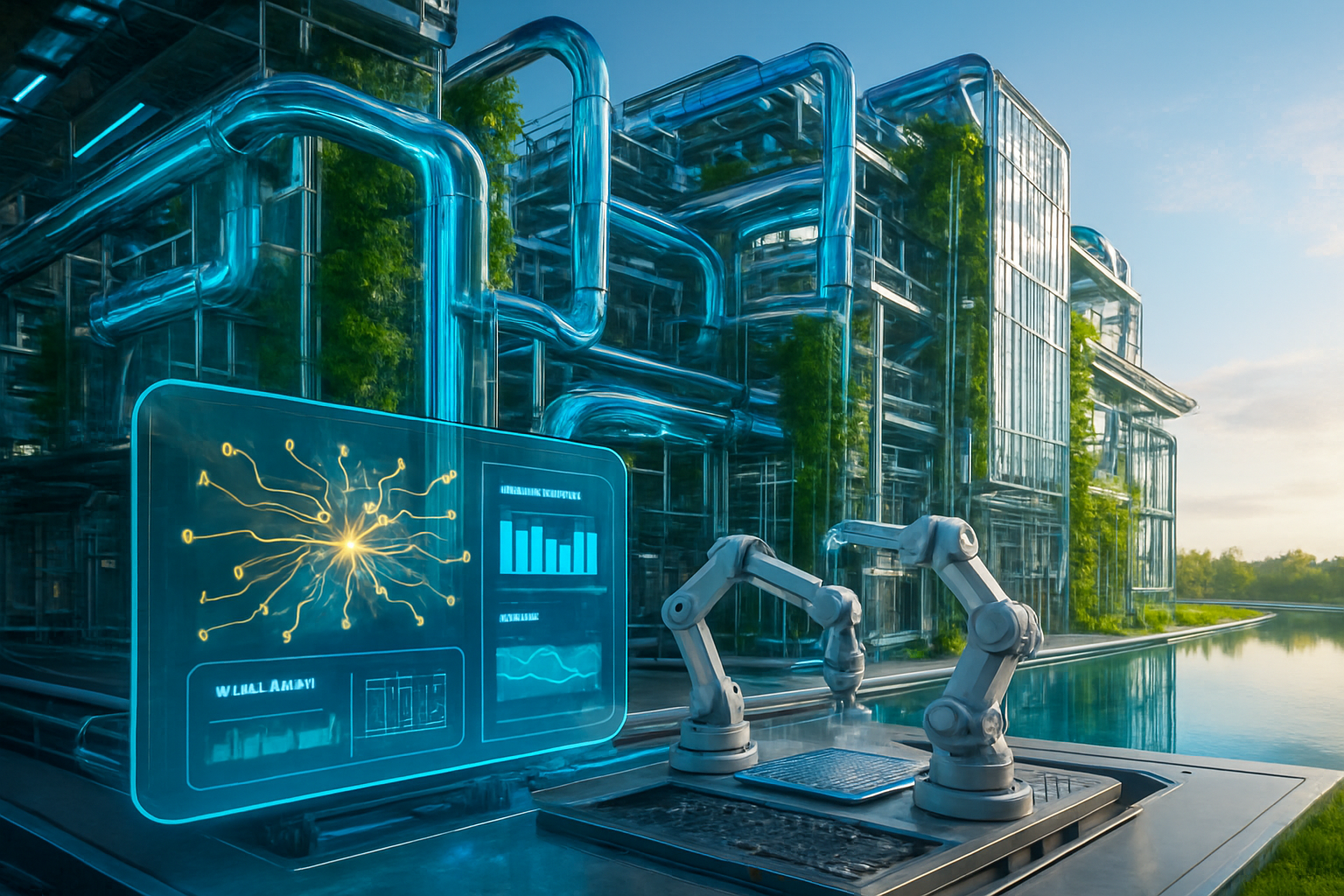
    The technical requirements of AI-specific data centers differ fundamentally from the traditional "cloud" facilities of the last decade. While a standard data center might consume 10 to 20 megawatts of power, the new "AI gigascale" campuses, such as the proposed "Project Stargate" by OpenAI and Oracle (NYSE:ORCL), are designed to consume upwards of five gigawatts—enough to power millions of homes. These facilities house high-density racks of GPUs that generate immense heat, necessitating cooling systems that "drink" millions of gallons of water daily. In drought-prone regions like Buckeye and Tucson, Arizona, the technical demand for up to 5 million gallons of water per day for a single campus has been labeled a "death sentence" for local aquifers by groups like the No Desert Data Center Coalition.

    To mitigate water usage, some developers have pivoted to air-cooled designs, but this shift has introduced a different technical nightmare for neighbors: noise. These systems rely on massive industrial fans and diesel backup generators that create a constant, low-frequency mechanical hum. In Prince William County, Virginia, residents describe this as a mental health hazard that persists 24 hours a day. Furthermore, the speed of development has outpaced the electrical grid’s capacity. Technical reports from grid operators like PJM Interconnection indicate that the surge in AI demand is forcing the reactivation of coal plants and the installation of gas turbines, such as the 33 turbines powering xAI’s "Colossus" cluster in Memphis, which has drawn fierce criticism for its local air quality impact.

    Initial reactions from the AI research community have been a mix of alarm and adaptation. While researchers acknowledge the desperate need for compute to achieve Artificial General Intelligence (AGI), many are now calling for a "decentralized" or "edge-heavy" approach to AI to reduce the reliance on massive centralized hubs. Industry experts at the 2025 AI Infrastructure Summit noted that the "brute force" era of building massive campuses in residential zones is likely over, as the social license to operate has evaporated in the face of skyrocketing utility bills and environmental degradation.

    Big Tech’s Strategic Retreat and the Competitive Pivot

    The growing pushback has created a volatile landscape for the world’s largest technology companies. Amazon (NASDAQ:AMZN), through its AWS division, suffered a major blow in December 2025 when it was forced to back out of "Project Blue" in Tucson after a year-long dispute over water rights and local zoning. Similarly, Alphabet Inc. (NASDAQ:GOOGL) withdrew a $1.5 billion proposal in Franklin Township, Indiana, after a coordinated "red-shirt" protest by residents who feared the industrialization of their rural community. These setbacks are not just PR hurdles; they represent significant delays in the "compute arms race" against rivals who may find friendlier jurisdictions.

    Microsoft (NASDAQ:MSFT) and Meta (NASDAQ:META) have attempted to get ahead of the backlash by promising "net-positive" water usage and investing in carbon-capture technologies, but the competitive advantage is shifting toward companies that can secure "off-grid" power. The pushback is also disrupting the market positioning of secondary players. Real estate investment trusts (REITs) like Equinix (NASDAQ:EQIX) and Digital Realty (NYSE:DLR) are finding it increasingly difficult to secure land in traditional "Data Center Alleys," leading to a spike in land prices in remote areas of the Midwest and the South.

    This disruption has also opened a door for startups focusing on "sovereign AI" and modular data centers. As the "Big Four" face legal injunctions and local ousters of pro-development officials, the strategic advantage is moving toward those who can build smaller, more efficient, and less intrusive facilities. The "frenzy" has essentially forced a market correction, where the cost of local opposition is finally being priced into the valuation of AI infrastructure projects.

    A Watershed Moment for the Broader AI Landscape

    The significance of this movement cannot be overstated; it marks the first time that the physical footprint of the digital world has faced a sustained, successful populist revolt. For years, the "cloud" was an abstract concept for most Americans. In 2025, it became a tangible neighbor that consumes local water, raises electricity rates by 10% to 14% to fund grid upgrades, and dominates the skyline with windowless grey boxes. This shift from "digital progress" to "industrial nuisance" mirrors the historical pushback against the expansion of railroads and interstate highways in the 20th century.

    Wider concerns regarding "environmental racism" have also come to the forefront. In Memphis and South Fulton, Georgia, activists have pointed out that fossil-fuel-powered data centers are disproportionately sited near minority communities, leading to a national call to action. In December 2025, a coalition of over 230 environmental groups, including Greenpeace, sent a formal letter to Congress demanding a national moratorium on new data centers until federal sustainability and "ratepayer protection" standards are enacted. This mirrors previous AI milestones where the focus shifted from technical capability to ethical and societal impact.

    The comparison to the "crypto-mining" backlash of 2021-2022 is frequent, but the AI data center pushback is far more widespread and legally sophisticated. Communities are now winning in court by citing "procedural failures" in how local governments use non-disclosure agreements (NDAs) to hide the identity of tech giants during the planning phases. New legislation in states like New Jersey and Oregon now requires real-time disclosure of water and energy usage, effectively ending the era of "secret" data center deals.

    The Future: Nuclear Power and Federal Intervention

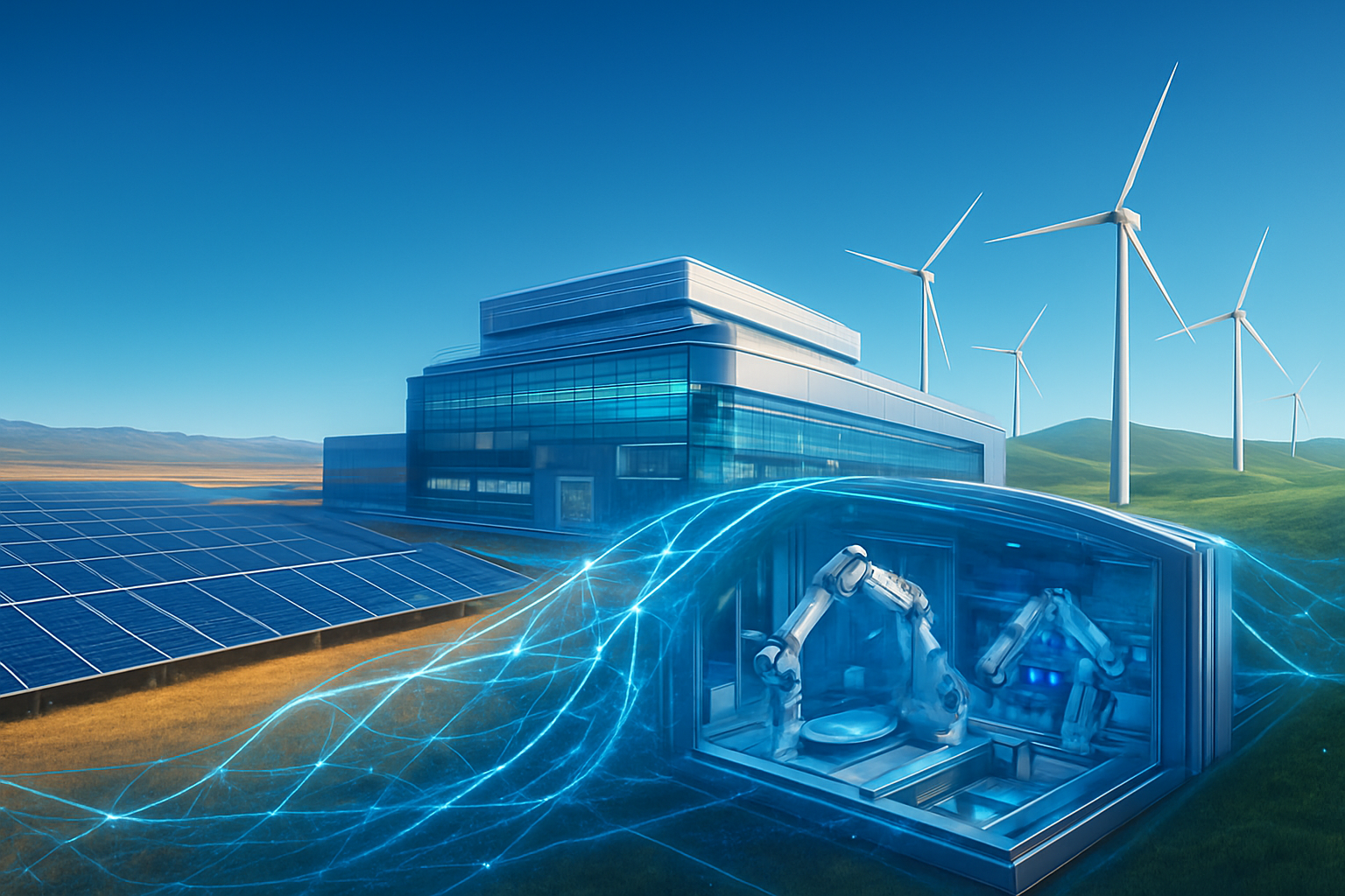
    Looking ahead, the industry is moving toward radical new energy solutions to bypass local grid concerns. We are likely to see a surge in "behind-the-meter" power generation, specifically Small Modular Reactors (SMRs) and fusion experiments. Microsoft’s recent deals to restart dormant nuclear plants are just the beginning; by 2027, experts predict that the most successful AI campuses will be entirely self-contained "energy islands" that do not draw from the public grid. This would alleviate the primary concern of residential rate spikes, though it may introduce new fears regarding nuclear safety.

    In the near term, the challenge remains one of geography and zoning. Potential applications for AI in urban planning and "smart city" management are being hindered by the very animosity the industry has created. If the "frenzy" continues to ignore local sentiment, experts predict a federal intervention. The Department of Energy is already considering "National Interest Electric Transmission Corridors" that could override local opposition, but such a move would likely trigger a constitutional crisis over state and local land-use rights.

    The next 12 to 18 months will be defined by a "flight to the remote." Developers are already scouting locations in the high plains and northern territories where the climate provides natural cooling and the population density is low. However, even these areas are beginning to organize, realizing that the "jobs" promised by data centers—often fewer than 50 permanent roles for a multi-billion dollar facility—do not always outweigh the environmental costs.

    Summary of the Great AI Infrastructure Clash

    The local pushback against AI data centers in 2025 has fundamentally altered the trajectory of the industry. The key takeaways are clear: the era of unchecked "industrialization" of residential areas is over, and the hidden costs of AI—water, power, and peace—are finally being brought into the light. The movement has forced a pivot toward transparency, with states like Minnesota and Texas leading the way in "Ratepayer Protection" laws that ensure tech giants, not citizens, foot the bill for grid expansion.

    This development will be remembered as a significant turning point in AI history—the moment the "virtual" world was forced to negotiate with the "physical" one. The long-term impact will be a more efficient, albeit slower-growing, AI infrastructure that is forced to innovate in energy and cooling rather than just scaling up. In the coming months, watch for the results of the 2026 local elections, where "data center reform" is expected to be a top-tier issue for voters across the country. The "frenzy" may be cooling, but the battle for the backyard of the AI age is only just beginning.


    This content is intended for informational purposes only and represents analysis of current AI developments.

    TokenRing AI delivers enterprise-grade solutions for multi-agent AI workflow orchestration, AI-powered development tools, and seamless remote collaboration platforms.
    For more information, visit https://www.tokenring.ai/.

  • Sustainability in the Fab: The Race for Net-Zero Water and Energy

    Sustainability in the Fab: The Race for Net-Zero Water and Energy

    As the artificial intelligence "supercycle" continues to accelerate, driving global chip sales to a record $72.7 billion in October 2025, the semiconductor industry is facing an unprecedented resource crisis. The transition to 2nm and 1.4nm manufacturing nodes has proven to be a double-edged sword: while these chips power the next generation of generative AI, their production requires up to 2.3 times more water and 3.5 times more electricity than previous generations. In response, the world’s leading foundries have transformed their operations, turning the "mega-fab" into a laboratory for radical sustainability and "Net-Zero" resource management.

    This shift has moved beyond corporate social responsibility into the realm of operational necessity. In late 2025, water scarcity in hubs like Arizona and Taiwan has made "Net-Positive" water status—where a company returns more water to the ecosystem than it withdraws—the new gold standard for the industry. From Micron’s billion-dollar conservation funds to TSMC’s pioneering reclaimed water plants, the race to build the first truly circular semiconductor ecosystem is officially on, powered by the very AI these facilities were built to produce.

    The Technical Frontiers of Ultrapure Water and Zero Liquid Discharge

    At the heart of the sustainability push is the management of Ultrapure Water (UPW), a substance thousands of times cleaner than pharmaceutical-grade water. In the 2nm era, even a "killer particle" as small as 10nm can ruin a wafer, making the purification process more intensive than ever. To combat the waste associated with this purity, companies like Micron Technology (NASDAQ: MU) have committed to a $1 billion sustainability initiative. As of late 2025, Micron has already deployed over $406 million of this fund, achieving a 66% global water conservation rate. Their planned $100 billion mega-fab in Clay, New York, is currently implementing a "Green CHIPS" framework designed to achieve near-100% water conservation through massive internal recycling loops.

    Taiwan Semiconductor Manufacturing Company (NYSE: TSM), or TSMC, has taken a different but equally ambitious path with its industrial-scale reclaimed water plants. In Taiwan’s Southern Taiwan Science Park, TSMC’s facilities reached a milestone in 2025, supplying nearly 67,000 metric tons of recycled water daily. Meanwhile, at its Phoenix, Arizona campus, TSMC broke ground in August 2025 on a new 15-acre Industrial Reclamation Water Plant (IRWP). Once fully operational, this facility is designed to recycle 90% of the fab's industrial wastewater, reducing the daily demand of a single fab from 4.75 million gallons to under 1.2 million gallons—a critical achievement in the water-stressed American Southwest.

    Technologically, these "Net-Zero" systems rely on a complex hierarchy of purification. Modern fabs in 2025 utilize segmented waste streams, separating chemical rinses from hydrofluoric acid waste to treat them individually. Advanced techniques such as Pulse-Flow Reverse Osmosis (PFRO) and Electrodeionization (EDI) are now standard, allowing for 98% water recovery. Furthermore, the introduction of 3D-printed spacers in membrane filtration—a technology backed by Micron—has significantly reduced the energy required to push water through these microscopic filters, addressing the energy-water nexus head-on.

    Competitive Advantages and the Rise of 'Green' Silicon

    The push for sustainability is reshaping the competitive landscape for chipmakers like Intel (NASDAQ: INTC) and Samsung Electronics (KRX: 005930). Intel’s Q4 2025 update confirmed that its 18A (1.8nm) process node is not just a performance leader but a sustainability one, delivering a 40% reduction in power consumption compared to older nodes. By simplifying the processing flow by 44% through advanced EUV lithography, Intel has reduced the total material intensity of its most advanced chips. This "green silicon" approach provides a strategic advantage as major customers like Microsoft (NASDAQ: MSFT) and NVIDIA (NASDAQ: NVDA) now demand verified "carbon and water receipts" for every wafer to meet their own 2030 net-zero goals.

    Samsung has countered with its own massive milestones, announcing in October 2025 that it achieved the UL Solutions "Zero Waste to Landfill" Platinum designation across all its global manufacturing sites. In South Korea, Samsung’s collaboration with the Ministry of Environment now supplies 120,000 tonnes of reclaimed water per day to its Giheung and Hwaseong fabs. For these giants, sustainability is no longer just about compliance; it is a market positioning tool. Foundries that can guarantee production continuity in water-stressed regions while lowering the carbon footprint of the end product are winning the lion's share of long-term supply contracts from sustainability-conscious tech titans.

    AI as the Architect of the Sustainable Fab

    Perhaps the most poetic development of 2025 is the use of AI to optimize the very factories that create it. "Agentic AI" ecosystems, such as those launched by Schneider Electric (EPA: SU) in mid-2025, now act as autonomous stewards of fab resources. these AI agents monitor thousands of sensors in real-time, making independent adjustments to chiller settings, HVAC airflow, and ultrapure water flow rates. This has led to an average 20% improvement in operational energy efficiency across modern mega-fabs.

    Digital Twin technology has also become a standard requirement for new construction. Companies like Applied Materials (NASDAQ: AMAT) are utilizing their EPIC platform to create high-fidelity virtual replicas of the manufacturing process. By simulating gas usage and chemical reactions before a single wafer is processed, these AI-driven systems have achieved a 50% reduction in gas usage and significantly reduced wafer scrap. This "yield-as-sustainability" metric is crucial; by reducing the number of defective chips, fabs indirectly save millions of gallons of water and megawatts of power that would have been "wasted" on failed silicon.

    The Road to 2030: Challenges and Next Steps

    Looking ahead, the industry faces the daunting task of scaling these "Net-Zero" successes as they move toward 1.4nm and 1nm nodes. While 90% water recycling is achievable today, the final 10%—often referred to as the "brine challenge"—remains difficult and energy-intensive to treat. Experts predict that the next three years will see a surge in investment toward Zero Liquid Discharge (ZLD) technologies that can evaporate and crystallize the final waste streams into solid minerals, leaving no liquid waste behind.

    Furthermore, the integration of AI into the power grid itself is a major focus for 2026. The U.S. Department of Energy’s "Genesis Mission," launched in December 2025, aims to use AI to coordinate the massive energy demands of semiconductor clusters with renewable energy availability. As fabs become larger and more complex, the ability to "load-balance" a mega-fab against a city’s power grid will be the next great frontier in industrial AI applications.

    A New Era for Semiconductor Manufacturing

    The semiconductor industry's evolution in 2025 marks a definitive end to the era of "growth at any cost." The race for Net-Zero water and energy has proven that high-performance computing and environmental stewardship are not mutually exclusive. Through a combination of radical transparency, multi-billion dollar infrastructure investments, and the deployment of agentic AI, the industry is setting a blueprint for how heavy industry can adapt to a resource-constrained world.

    As we move into 2026, the focus will shift from building these sustainable systems to proving their long-term resilience. The success of TSMC’s Arizona plant and Micron’s New York mega-fab will be the ultimate litmus test for the industry's green ambitions. For now, the "Sustainability in the Fab" movement has demonstrated that the most important breakthrough in the AI era might not be the chips themselves, but the sustainable way in which we make them.


    This content is intended for informational purposes only and represents analysis of current AI developments.

    TokenRing AI delivers enterprise-grade solutions for multi-agent AI workflow orchestration, AI-powered development tools, and seamless remote collaboration platforms.
    For more information, visit https://www.tokenring.ai/.

  • The Great AI Reckoning: Why the $600 Billion ROI Gap Is Rattling Markets in Late 2025

    The Great AI Reckoning: Why the $600 Billion ROI Gap Is Rattling Markets in Late 2025

    As the final weeks of 2025 unfold, the artificial intelligence industry finds itself at a precarious crossroads. While the technological leaps of the past year have been nothing short of extraordinary, a growing chorus of economists and financial analysts are sounding the alarm on what they call the "Great AI Reckoning." Despite a historic $400 billion annual infrastructure splurge by the world’s largest tech titans, the promised "productivity miracle" has yet to materialize on corporate balance sheets, leading to an intensifying debate over whether the AI boom is entering a dangerous bubble phase.

    The tension lies in a staggering disconnect: while NVIDIA (NASDAQ:NVDA) and other hardware providers report record-breaking revenues from the sale of AI chips, the enterprises buying these capabilities are struggling to turn them into profit. This "ROI Gap"—the distance between capital investment and actual revenue generated by AI applications—has ballooned to an estimated $600 billion. As of December 24, 2025, the market is shifting from a state of "AI euphoria" to a disciplined "show me the money" phase, where the environmental and financial costs of the AI revolution are finally being weighed against their tangible benefits.

    The $400 Billion Infrastructure Surge

    The technical scale of the AI buildout in 2025 is unprecedented in industrial history. The "Big Four" hyperscalers—Amazon (NASDAQ:AMZN), Alphabet (NASDAQ:GOOGL), Microsoft (NASDAQ:MSFT), and Meta (NASDAQ:META)—have collectively pushed their annual capital expenditure (CapEx) toward the $320 billion to $400 billion range. This spending is primarily directed toward "AI factories": massive, liquid-cooled data center clusters designed to house hundreds of thousands of next-generation GPUs. Microsoft’s "Stargate" initiative, a multi-phase project in collaboration with OpenAI, represents the pinnacle of this ambition, aiming to build a supercomputing complex that dwarfs any existing infrastructure.

    Technically, the 2025 era of AI has moved beyond the simple chatbots of 2023. We are now seeing the deployment of "Trillium" TPUs from Google and "Trainium2" chips from Amazon, which offer significant improvements in energy efficiency and training speed over previous generations. However, the complexity of these systems has also surged. The industry has shifted toward "Agentic AI"—systems capable of autonomous reasoning and multi-step task execution—which requires significantly higher inference costs than earlier models. Initial reactions from the research community have been mixed; while the technical capabilities of models like Llama 4 and GPT-5 are undeniable, experts at MIT have noted that the "marginal utility" of adding more compute is beginning to face diminishing returns for standard enterprise tasks.

    The Hyperscaler Paradox and Competitive Survival

    The current market landscape is dominated by a "Hyperscaler Paradox." Companies like Microsoft and Google are essentially forced to spend tens of billions on infrastructure just to maintain their competitive positions, even if the immediate ROI is unclear. For these giants, the risk of under-investing and losing the AI race is viewed as far more catastrophic than the risk of over-investing. This has created a "circular revenue" cycle where hyperscalers fund AI startups, who then use that capital to buy compute time back from the hyperscalers, artificially inflating growth figures in the eyes of some skeptics.

    NVIDIA remains the primary beneficiary of this cycle, with its data center revenue continuing to defy gravity. However, the competitive implications are shifting. As the cost of training frontier models reaches the $10 billion mark, the barrier to entry has become insurmountable for all but a handful of firms. This consolidation of power has led to concerns about an "AI Oligopoly," where a few companies control the fundamental "compute utility" of the global economy. Meanwhile, smaller AI labs are finding it increasingly difficult to secure the necessary hardware, leading to a wave of "acqui-hires" by tech giants looking to absorb talent without the regulatory scrutiny of a full merger.

    Environmental Costs and the 95% Failure Rate

    Beyond the financial balance sheets, the wider significance of the AI boom is being measured in megawatts and metric tons of carbon. By late 2025, global power consumption for AI has reached 23 gigawatts, officially surpassing the energy usage of the entire Bitcoin mining industry. In the United States, data centers now consume over 10% of the total electricity supply in six states, with Virginia leading at a staggering 25%. The environmental impact is no longer a peripheral concern; analysts from Barclays (NYSE:BCS) report that AI data centers generated up to 80 million metric tons of CO2 in 2025 alone—a footprint comparable to the city of New York.

    Perhaps more damaging to the "AI narrative" is the high failure rate of corporate AI projects. A landmark December 2025 report from MIT revealed that 95% of enterprise AI pilots have failed to deliver a measurable ROI. Most initiatives remain "stuck in the lab," plagued by data privacy hurdles, high inference costs, and the sheer difficulty of integrating AI into legacy workflows. While 88% of companies claim to be "using" AI, only about 13% to 35% have moved these projects into full-scale production. This has led Goldman Sachs (NYSE:GS) to warn that we are entering a "Phase 3" transition, where investors will ruthlessly penalize any firm that cannot demonstrate tangible earnings gains from their AI investments.

    The Road to 2027: Deceleration or Breakthrough?

    Looking ahead, experts predict a significant shift in how AI is developed and deployed. The "brute force" era of scaling—simply adding more chips and more data—is expected to give way to a focus on "algorithmic efficiency." Near-term developments are likely to center on small, specialized models that can run on-device or on local servers, reducing the reliance on massive, energy-hungry data centers. The goal is to lower the "cost per intelligence unit," making AI more accessible to medium-sized enterprises that currently find the technology cost-prohibitive.

    The primary challenge for 2026 and 2027 will be the "Power Wall." With the global grid already strained, tech companies are increasingly looking toward nuclear energy and small modular reactors (SMRs) to power their future expansion. If the industry can overcome these energy constraints and solve the "ROI Gap" through more efficient software, the current infrastructure buildout may be remembered as the foundation of a new industrial revolution. If not, analysts at Sequoia Capital warn that a "sharp deceleration" in CapEx growth is inevitable, which could lead to a painful market correction for the entire tech sector.

    Summary of the Great AI Reckoning

    The AI landscape of late 2025 is a study in contradictions. We are witnessing the most rapid technological advancement in history, supported by the largest capital deployment ever seen, yet the economic justification for this spending remains elusive for the vast majority of businesses. The key takeaway from 2025 is that "AI is real, but the bubble might be too." While the foundational infrastructure being built today will likely power the global economy for decades, much of the speculative capital currently flooding the market may be incinerated in the coming year as unprofitable projects are shuttered.

    As we move into 2026, the industry must transition from "hype" to "utility." The significance of this period in AI history cannot be overstated; it is the moment when the technology must finally prove its worth in the real world. Investors and industry watchers should keep a close eye on quarterly earnings reports from non-tech Fortune 500 companies—the true indicator of AI’s success will not be NVIDIA’s chip sales, but whether a manufacturing firm in Ohio or a retail chain in London can finally show that AI has made them more profitable.


    This content is intended for informational purposes only and represents analysis of current AI developments.

    TokenRing AI delivers enterprise-grade solutions for multi-agent AI workflow orchestration, AI-powered development tools, and seamless remote collaboration platforms.
    For more information, visit https://www.tokenring.ai/.

  • The Silicon Thirst: Can the AI Revolution Survive Its Own Environmental Footprint?

    The Silicon Thirst: Can the AI Revolution Survive Its Own Environmental Footprint?

    As of December 22, 2025, the semiconductor industry finds itself at a historic crossroads, grappling with a "green paradox" that threatens to derail the global AI gold rush. While the latest generation of 2nm artificial intelligence chips offers unprecedented energy efficiency during operation, the environmental cost of manufacturing these silicon marvels has surged to record levels. The industry is currently facing a dual crisis of resource scarcity and regulatory pressure, as the massive energy and water requirements of advanced fabrication facilities—or "mega-fabs"—clash with global climate commitments and local environmental limits.

    The immediate significance of this sustainability challenge cannot be overstated. With the demand for generative AI showing no signs of slowing, the carbon footprint of chip manufacturing has become a critical bottleneck. Leading firms are no longer just competing on transistor density or processing speed; they are now racing to secure "green" energy contracts and pioneer water-reclamation technologies to satisfy both increasingly stringent government regulations and the strict sustainability mandates of their largest customers.

    The High Cost of the 2nm Frontier

    Manufacturing at the 2nm and 1.4nm nodes, which became the standard for flagship AI accelerators in late 2024 and 2025, is substantially more resource-intensive than any previous generation of silicon. Technical data from late 2025 confirms that the transition from mature 28nm nodes to cutting-edge 2nm processes has resulted in a 3.5x increase in electricity consumption and a 2.3x increase in water usage per wafer. This spike is driven by the extreme complexity of sub-2nm designs, which can require over 4,000 individual process steps and frequent "rinsing" cycles using millions of gallons of Ultrapure Water (UPW) to prevent microscopic defects.

    The primary driver of this energy surge is the adoption of High-NA (Numerical Aperture) Extreme Ultraviolet (EUV) lithography. The latest EXE:5200 scanners from ASML (NASDAQ: ASML), which are now the backbone of advanced pilot lines, consume approximately 1.4 Megawatts (MW) of power per unit—enough to power a small town. While these machines are energy hogs, industry experts point to a "sustainability win" in their resolution capabilities: by enabling "single-exposure" patterning, High-NA tools eliminate several complex multi-patterning steps required by older EUV models, potentially saving up to 200 kWh per wafer and significantly reducing chemical waste.

    Initial reactions from the AI research community have been mixed. While researchers celebrate the performance gains of chips like the NVIDIA (NASDAQ: NVDA) "Rubin" architecture, environmental groups have raised alarms. A 2025 report from Greenpeace highlighted a fourfold increase in carbon emissions from AI chip manufacturing over the past two years, noting that the sector's electricity consumption for AI chipmaking alone soared to nearly 984 GWh in 2024. This has sparked a debate over "embodied emissions"—the carbon generated during the manufacturing phase—which now accounts for nearly 30% of the total lifetime carbon footprint of an AI-driven data center.

    Corporate Mandates and the "Carbon Receipt"

    The environmental crisis has fundamentally altered the strategic landscape for tech giants and semiconductor foundries. By late 2025, "Big Tech" firms including Microsoft (NASDAQ: MSFT), Amazon (NASDAQ: AMZN), and Alphabet (NASDAQ: GOOGL) have begun using their massive purchasing power to force sustainability down the supply chain. Microsoft, for instance, implemented a 2025 Supplier Code of Conduct that requires high-impact suppliers like TSMC (NYSE: TSM) and Intel (NASDAQ: INTC) to transition to 100% carbon-free electricity by 2030. This has led to the rise of the "carbon receipt," where foundries must provide verified, chip-level emissions data for every wafer produced.

    This shift has created a new competitive hierarchy. Intel has aggressively marketed its 18A node as the "world's most sustainable advanced node," highlighting its achievement of "Net Positive Water" status in the U.S. and India. Meanwhile, TSMC has responded to client pressure by accelerating its RE100 timeline, aiming for 100% renewable energy by 2040—a decade earlier than its previous goal. For NVIDIA and AMD (NASDAQ: AMD), the challenge lies in managing Scope 3 emissions; while their architectures are vastly more efficient for AI inference, their supply chain emissions have doubled in some cases due to the sheer volume of hardware being manufactured to meet AI demand.

    Smaller startups and secondary players are finding themselves at a disadvantage in this new "green" economy. The cost of implementing advanced water reclamation systems and securing long-term renewable energy power purchase agreements (PPAs) is astronomical. Major players like Samsung (KRX: 005930) are leveraging their scale to deploy "Digital Twin" technology—using AI to simulate and optimize fab airflow and power usage—which has improved operational energy efficiency by nearly 20% compared to traditional methods.

    Global Regulation and the PFAS Ticking Clock

    The broader significance of the semiconductor sustainability crisis is reflected in a tightening global regulatory net. In the European Union, the transition toward a "Chips Act 2.0" in late 2025 has introduced mandatory "Chip Circularity" requirements, forcing manufacturers to provide roadmaps for e-waste recovery and the reuse of rare earth metals as a condition for state aid. In the United States, while some environmental reviews were streamlined to speed up fab construction, the EPA is finalized new effluent limitation guidelines specifically for the semiconductor industry to curb the discharge of "forever chemicals."

    One of the most daunting challenges facing the industry in late 2025 is the phase-out of Per- and polyfluoroalkyl substances (PFAS). These chemicals are essential for advanced lithography and cooling but are under intense scrutiny from the European Chemicals Agency (ECHA). While the industry has been granted "essential use" exemptions, a mandatory 5-to-12-year phase-out window is now in effect. This has triggered a desperate search for alternatives, leading to a 2025 breakthrough in PFAS-free Metal-Oxide Resists (MORs), which have begun replacing traditional chemicals in 2nm production lines.

    This transition mirrors previous industrial milestones, such as the removal of lead from electronics, but at a much more compressed and high-stakes scale. The "Green Paradox" of AI—where the technology is both a primary consumer of resources and a vital tool for environmental optimization—has become the defining tension of the mid-2020s. The industry's ability to resolve this paradox will determine whether the AI revolution is seen as a sustainable leap forward or a resource-intensive bubble.

    The Horizon: AI-Optimized Fabs and Circular Silicon

    Looking toward 2026 and beyond, the industry is betting heavily on circular economy principles and AI-driven optimization to balance the scales. Near-term developments include the wider deployment of "free cooling" architectures for High-NA EUV tools, which use 32°C water instead of energy-intensive chillers, potentially reducing the power required for laser cooling by 75%. We also expect to see the first commercial-scale implementations of "chip recycling" programs, where precious metals and even intact silicon components are salvaged from decommissioned AI servers.

    Potential applications on the horizon include "bio-synthetic" cleaning agents and more advanced water-recycling technologies that could allow fabs to operate in even the most water-stressed regions without impacting local supplies. However, the challenge of raw material extraction remains. Experts predict that the next major hurdle will be the environmental impact of mining the rare earth elements required for the high-performance magnets and capacitors used in AI hardware.

    The industry's success will likely hinge on the development of "Digital Twin" fabs that are fully integrated with local smart grids, allowing them to adjust power consumption in real-time based on renewable energy availability. Predictors suggest that by 2030, the "sustainability score" of a semiconductor node will be as important to a company's market valuation as its processing power.

    A New Era of Sustainable Silicon

    The environmental sustainability challenges facing the semiconductor industry in late 2025 represent a fundamental shift in the tech landscape. The era of "performance at any cost" has ended, replaced by a new paradigm where resource efficiency is a core component of technological leadership. Key takeaways from this year include the massive resource requirements of 2nm manufacturing, the rising power of "Big Tech" to dictate green standards, and the looming regulatory deadlines for PFAS and carbon reporting.

    In the history of AI, this period will likely be remembered as the moment when the physical reality of hardware finally caught up with the virtual ambitions of software. The long-term impact of these sustainability efforts will be a more resilient, efficient, and transparent global supply chain. However, the path forward is fraught with technical and economic hurdles that will require unprecedented collaboration between competitors.

    In the coming weeks and months, industry watchers should keep a close eye on the first "Environmental Product Declarations" (EPDs) from NVIDIA and TSMC, as well as the progress of the US EPA’s final rulings on PFAS discharge. These developments will provide the first real data on whether the industry’s "green" promises can keep pace with the insatiable thirst of the AI revolution.


    This content is intended for informational purposes only and represents analysis of current AI developments.

    TokenRing AI delivers enterprise-grade solutions for multi-agent AI workflow orchestration, AI-powered development tools, and seamless remote collaboration platforms.
    For more information, visit https://www.tokenring.ai/.

  • The Green Paradox: Can the AI Boom Survive the Semiconductor Industry’s Rising Resource Demands?

    The Green Paradox: Can the AI Boom Survive the Semiconductor Industry’s Rising Resource Demands?

    As of December 19, 2025, the global technology sector is grappling with a profound "green paradox." While artificial intelligence is being hailed as a critical tool for solving climate change, the physical manufacturing of the chips that power it—such as Nvidia’s Blackwell and Blackwell Ultra architectures—has pushed the semiconductor industry’s energy and water consumption to unprecedented levels. This week, industry leaders and environmental regulators have signaled a major pivot toward "Sustainable Silicon," as the resource-heavy requirements of 3nm and 2nm fabrication nodes begin to clash with global net-zero commitments.

    The immediate significance of this shift cannot be overstated. With the AI chip market continuing its meteoric rise, the environmental footprint of a single leading-edge wafer has nearly tripled compared to a decade ago. This has forced the world's largest chipmakers to adopt radical new technologies, from AI-driven "Digital Twin" factories to closed-loop water recycling systems, in an effort to decouple industrial growth from environmental degradation.

    Engineering the Closed-Loop Fab: Technical Breakthroughs in 2025

    The technical challenge of modern chip fabrication lies in the extreme complexity of the latest manufacturing nodes. As companies like TSMC (NYSE: TSM) and Samsung (KRX: 005930) move toward 2nm production, the number of mask layers and chemical processing steps has increased significantly. To combat the resulting resource drain, the industry has turned to "Counterflow Reverse Osmosis," a breakthrough in Ultra Pure Water (UPW) management. This technology now allows fabs to recycle up to 90% of their wastewater directly back into the sensitive wafer-rinsing stages—a feat previously thought impossible due to the risk of microscopic contamination.

    Energy consumption remains the industry's largest hurdle, primarily driven by Extreme Ultraviolet (EUV) lithography tools manufactured by ASML (NASDAQ: ASML). These machines, which are essential for printing the world's most advanced transistors, consume roughly 1.4 megawatts of power each. To mitigate this, TSMC has fully deployed its "EUV Dynamic Power Saving" program this year. By using real-time AI to pulse the EUV light source only when necessary, the system has successfully reduced tool-level energy consumption by 8% without sacrificing throughput.

    Furthermore, the industry is seeing a surge in AI-driven yield optimization. By utilizing deep learning for defect detection, manufacturers have reported a 40% reduction in defect rates on 3nm lines. This efficiency is a sustainability win: by catching errors early, fabs prevent the "waste" of thousands of gallons of UPW and hundreds of kilowatts of energy that would otherwise be spent processing a defective wafer. Industry experts have praised these advancements, noting that the "Intelligence-to-Efficiency" loop is finally closing, where AI chips are being used to optimize the very factories that produce them.

    The Competitive Landscape: Tech Giants Race for 'Green' Dominance

    The push for sustainability is rapidly becoming a competitive differentiator for the world's leading foundries and integrated device manufacturers. Intel (NASDAQ: INTC) has emerged as an early leader in renewable energy adoption, announcing this month that it has achieved 98% global renewable electricity usage. Intel’s "Net Positive Water" goal is also ahead of schedule, with its facilities in the United States and India already restoring more water to local ecosystems than they consume. This positioning is a strategic advantage as cloud providers seek to lower their Scope 3 emissions.

    For Nvidia (NASDAQ: NVDA), the sustainability of the fabrication process is now a core component of its market positioning. As the primary customer for TSMC’s most advanced nodes, Nvidia is under pressure from its own enterprise clients to provide "Green AI" solutions. The massive die size of Nvidia's Blackwell GPUs means fewer chips can be harvested from a single wafer, making each chip more "resource-expensive" than a standard mobile processor. In response, Nvidia has partnered with Samsung to develop Digital Twins of entire fabrication plants, using over 50,000 GPUs to simulate and optimize airflow and power loads, improving overall operational efficiency by an estimated 20%.

    This shift is also disrupting the supply chain for equipment manufacturers like Applied Materials (NASDAQ: AMAT) and Lam Research (NASDAQ: LRCX). There is a growing demand for "dry" lithography and etching solutions that eliminate the need for water-intensive processes. Startups focusing on sustainable chemistry are also finding new opportunities as the industry moves away from "forever chemicals" (PFAS) in response to tightening global regulations.

    The Regulatory Hammer and the Broader AI Landscape

    The broader significance of these developments is underscored by a new wave of international regulations. As of November 2024, the Global Electronics Council introduced stricter EPEAT criteria for semiconductors, and in 2025, the European Union's "Digital Product Passport" (DPP) became a mandatory requirement for chips sold in the region. This regulation forces manufacturers to provide a transparent "cradle-to-gate" account of the carbon and water footprint for every chip, effectively making sustainability a prerequisite for market access in Europe.

    This regulatory environment marks a departure from previous AI milestones, where the focus was almost entirely on performance and "flops per watt." Today, the conversation has shifted to the "embedded" environmental cost of the hardware itself. Concerns are mounting that the resource intensity of AI could lead to localized water shortages or energy grid instability in semiconductor hubs like Arizona, Taiwan, and South Korea. This has led to a comparison with the early days of data center expansion, but at a much more concentrated and resource-intensive scale.

    The Semiconductor Climate Consortium (SCC) has also launched a standardized Scope 3 reporting framework this year. This compels fabs to account for the carbon footprint of their entire supply chain, from raw silicon mining to the production of specialty gases. By standardizing these metrics, the industry is moving toward a future where "green silicon" could eventually command a price premium over traditionally manufactured chips.

    Looking Ahead: The Road to 2nm and Circularity

    In the near term, the industry is bracing for the transition to 2nm nodes, which is expected to begin in earnest in late 2026. While these nodes promise greater energy efficiency for the end-user, the fabrication process will be the most resource-intensive in history. Experts predict that the next major breakthrough will involve a move toward a "circular economy" for semiconductors, where rare-earth metals and silicon are reclaimed from decommissioned AI servers and fed back into the manufacturing loop.

    Potential applications on the horizon include the integration of small-scale modular nuclear reactors (SMRs) directly into fab campuses to provide a stable, carbon-free baseload of energy. Challenges remain, particularly in the elimination of PFAS, as many of the chemical substitutes currently under testing have yet to match the precision required for leading-edge nodes. However, the trajectory is clear: the semiconductor industry is moving toward a "Zero-Waste" model that treats water and energy as finite, precious resources rather than cheap industrial inputs.

    A New Era for Sustainable Computing

    The push for sustainability in semiconductor manufacturing represents a pivotal moment in the history of computing. The key takeaway from 2025 is that the AI revolution cannot be sustained by 20th-century industrial practices. The industry’s ability to innovate its way out of the "green paradox"—using AI to optimize the fabrication of AI—will determine the long-term viability of the current technological boom.

    As we look toward 2026, the industry's success will be measured not just by transistor density or clock speeds, but by gallons of water saved and carbon tons avoided. The shift toward transparent reporting and closed-loop manufacturing is a necessary evolution for a sector that has become the backbone of the global economy. Investors and consumers alike should watch for the first "Water-Positive" fab certifications and the potential for a "Green Silicon" labeling system to emerge in the coming months.


    This content is intended for informational purposes only and represents analysis of current AI developments.

    TokenRing AI delivers enterprise-grade solutions for multi-agent AI workflow orchestration, AI-powered development tools, and seamless remote collaboration platforms.
    For more information, visit https://www.tokenring.ai/.

  • Powering the Singularity: DOE and Tech Titans Launch ‘Genesis Mission’ to Solve AI’s Energy Crisis

    Powering the Singularity: DOE and Tech Titans Launch ‘Genesis Mission’ to Solve AI’s Energy Crisis

    In a landmark move to secure the future of American computing power, the U.S. Department of Energy (DOE) officially inaugurated the "Genesis Mission" on December 18, 2025. This massive public-private partnership unites the federal government's scientific arsenal with the industrial might of tech giants including Amazon.com, Inc. (NASDAQ: AMZN), Alphabet Inc. (NASDAQ: GOOGL), and Microsoft Corporation (NASDAQ: MSFT). Framed by the administration as a "Manhattan Project-scale" endeavor, the mission aims to solve the single greatest bottleneck facing the artificial intelligence revolution: the staggering energy consumption of next-generation semiconductors and the data centers that house them.

    The Genesis Mission arrives at a critical juncture where the traditional power grid is struggling to keep pace with the exponential growth of AI workloads. By integrating the high-performance computing resources of all 17 DOE National Laboratories with the secure cloud infrastructures of the "Big Three" hyperscalers, the initiative seeks to create a unified national AI science platform. This collaboration is not merely about scaling up; it is a strategic effort to achieve "American Energy Dominance" by leveraging AI to design, license, and deploy radical new energy solutions—ranging from advanced small modular reactors (SMRs) to breakthrough fusion technology—specifically tailored to fuel the AI era.

    Technical Foundations: The Architecture of Energy Efficiency

    The technical heart of the Genesis Mission is the American Science and Security Platform, a high-security "engine" that bridges federal supercomputers with private cloud environments. Unlike previous efforts that focused on general-purpose computing, the Genesis Mission is specifically optimized for "scientific foundation models." These models are designed to reason through complex physics and chemistry problems, enabling the co-design of microelectronics that are exponentially more efficient. A core component of this is the Microelectronics Energy Efficiency Research Center (MEERCAT), which focuses on developing semiconductors that utilize new materials beyond silicon to reduce power leakage and heat generation in AI training clusters.

    Beyond chip design, the mission introduces "Project Prometheus," a $6.2 billion venture led by Jeff Bezos that works alongside the DOE to apply AI to the physical economy. This includes the use of autonomous laboratories—facilities where AI-driven robotics can conduct experiments 24/7 without human intervention—to discover new superconductors and battery chemistries. These labs, funded by a recent $320 million DOE investment, are expected to shorten the development cycle for energy-dense materials from decades to months. Furthermore, the partnership is deploying AI-enabled digital twins of the national power grid to simulate and manage the massive, fluctuating loads required by next-generation GPU clusters from NVIDIA Corporation (NASDAQ: NVDA).

    Initial reactions from the AI research community have been overwhelmingly positive, though some experts note the unprecedented nature of the collaboration. Dr. Aris Constantine, a lead researcher in high-performance computing, noted that "the integration of federal datasets with the agility of commercial cloud providers like Microsoft and Google creates a feedback loop we’ve never seen. We aren't just using AI to find energy; we are using AI to rethink the very physics of how computers consume it."

    Industry Impact: The Race for Infrastructure Supremacy

    The Genesis Mission fundamentally reshapes the competitive landscape for tech giants and AI labs alike. For the primary cloud partners—Amazon, Google, and Microsoft—the mission provides a direct pipeline to federal research and a regulatory "fast track" for energy infrastructure. By hosting the American Science Cloud (AmSC), these companies solidify their positions as the indispensable backbones of national security and scientific research. This strategic advantage is particularly potent for Microsoft and Google, who are already locked in a fierce battle to integrate AI across every layer of their software and hardware stacks.

    The partnership also provides a massive boost to semiconductor manufacturers and specialized AI firms. Companies like NVIDIA Corporation (NASDAQ: NVDA), Advanced Micro Devices, Inc. (NASDAQ: AMD), and Intel Corporation (NASDAQ: INTC) stand to benefit from the DOE’s MEERCAT initiatives, which provide the R&D funding necessary to experiment with high-risk, high-reward chip architectures. Meanwhile, AI labs like OpenAI and Anthropic, who are also signatories to the mission’s MOUs, gain access to a more resilient and scalable energy grid, ensuring their future models aren't throttled by power shortages.

    However, the mission may disrupt traditional energy providers. As tech giants increasingly look toward "behind-the-meter" solutions like SMRs and private fusion projects to power their data centers, the reliance on centralized public utilities could diminish. This shift positions companies like Oracle Corporation (NYSE: ORCL), which has recently pivoted toward modular nuclear-powered data centers, as major players in a new "energy-as-a-service" market that bypasses traditional grid limitations.

    Broader Significance: AI and the New Energy Paradigm

    The Genesis Mission is more than just a technical partnership; it represents a pivot in the global AI race from software optimization to hardware and energy sovereignty. In the broader AI landscape, the initiative signals that the "low-hanging fruit" of large language models has been picked, and the next frontier lies in "embodied AI" and the physical sciences. By aligning AI development with national energy goals, the U.S. is signaling that AI leadership is inseparable from energy leadership.

    This development also raises significant questions regarding environmental impact and regulatory oversight. While the mission emphasizes "carbon-free" power through nuclear and fusion, the immediate reality involves a massive buildout of infrastructure that will place immense pressure on local ecosystems and resources. Critics have voiced concerns that the rapid deregulation proposed in the January 2025 Executive Order, "Removing Barriers to American Leadership in Artificial Intelligence," might prioritize speed over safety and environmental standards.

    Comparatively, the Genesis Mission is being viewed as the 21st-century equivalent of the Interstate Highway System—a foundational infrastructure project that will enable decades of economic growth. Just as the highway system transformed the American landscape and economy, the Genesis Mission aims to create a "digital-energy highway" that ensures the U.S. remains the global hub for AI innovation, regardless of the energy costs.

    Future Horizons: From SMRs to Autonomous Discovery

    Looking ahead, the near-term focus of the Genesis Mission will be the deployment of the first AI-optimized Small Modular Reactors. These reactors are expected to be co-located with major data center hubs by 2027, providing a steady, high-capacity power source that is immune to the fluctuations of the broader grid. In the long term, the mission’s "Transformational AI Models Consortium" (ModCon) aims to produce self-improving AI that can autonomously solve the remaining engineering hurdles of commercial fusion energy, potentially providing a "limitless" power source by the mid-2030s.

    The applications of this mission extend far beyond energy. The materials discovered in the autonomous labs could revolutionize everything from electric vehicle batteries to aerospace engineering. However, challenges remain, particularly in the realm of cybersecurity. Integrating the DOE’s sensitive datasets with commercial cloud platforms creates a massive attack surface that will require the development of new, AI-driven "zero-trust" security protocols. Experts predict that the next year will see a surge in public-private "red-teaming" exercises to ensure the Genesis Mission’s infrastructure remains secure from foreign interference.

    A New Chapter in AI History

    The Genesis Mission marks a definitive shift in how the world approaches the AI revolution. By acknowledging that the future of intelligence is inextricably linked to the future of energy, the U.S. Department of Energy and its partners in the private sector have laid the groundwork for a sustainable, high-growth AI economy. The mission successfully bridges the gap between theoretical research and industrial application, ensuring that the "Big Three"—Amazon, Google, and Microsoft—along with semiconductor leaders like NVIDIA, have the resources needed to push the boundaries of what is possible.

    As we move into 2026, the success of the Genesis Mission will be measured not just by the benchmarks of AI models, but by the stability of the power grid and the speed of material discovery. This initiative is a bold bet on the idea that AI can solve the very problems it creates, using its immense processing power to unlock the clean, abundant energy required for its own evolution. The coming months will be crucial as the first $320 million in funding is deployed and the "American Science Cloud" begins its initial operations, marking the start of a new era in the synergy between man, machine, and the atom.


    This content is intended for informational purposes only and represents analysis of current AI developments.

    TokenRing AI delivers enterprise-grade solutions for multi-agent AI workflow orchestration, AI-powered development tools, and seamless remote collaboration platforms.
    For more information, visit https://www.tokenring.ai/.

  • Oracle’s ARM Revolution: How A4 Instances and AmpereOne Are Redefining the AI Cloud

    Oracle’s ARM Revolution: How A4 Instances and AmpereOne Are Redefining the AI Cloud

    In a decisive move to reshape the economics of the generative AI era, Oracle (NYSE: ORCL) has officially launched its OCI Ampere A4 Compute instances. Powered by the high-density AmpereOne M processors, these instances represent a massive bet on ARM architecture as the primary engine for sustainable, cost-effective AI inferencing. By decoupling performance from the skyrocketing power demands of traditional x86 silicon, Oracle is positioning itself as the premier destination for enterprises looking to scale AI workloads without the "GPU tax" or the environmental overhead of legacy data centers.

    The arrival of the A4 instances marks a strategic pivot in the cloud wars of late 2025. As organizations move beyond the initial hype of training massive models toward the practical reality of daily inferencing, the need for high-throughput, low-latency compute has never been greater. Oracle’s rollout, which initially spans key global regions including Ashburn, Frankfurt, and London, offers a blueprint for how "silicon neutrality" and open-market ARM designs can challenge the proprietary dominance of hyperscale competitors.

    The Engineering of Efficiency: Inside the AmpereOne M Architecture

    At the heart of the A4 instances lies the AmpereOne M processor, a custom-designed ARM chip that prioritizes core density and predictable performance. Unlike traditional x86 processors from Intel (NASDAQ: INTC) or AMD (NASDAQ: AMD) that rely on simultaneous multithreading (SMT), AmpereOne utilizes single-threaded cores. This design choice eliminates the "noisy neighbor" effect, ensuring that each of the 96 physical cores in a Bare Metal A4 instance delivers consistent, isolated performance. With clock speeds locked at a steady 3.6 GHz—a 20% jump over the previous generation—the A4 is built for the high-concurrency demands of modern cloud-native applications.

    The technical specifications of the A4 are tailored for memory-intensive AI tasks. The architecture features a 12-channel DDR5 memory subsystem, providing a staggering 143 GB/s of bandwidth. This is complemented by 2 MB of private L2 cache per core and a 64 MB system-level cache, significantly reducing the latency bottlenecks that often plague large-scale AI models. For networking, the instances support up to 100 Gbps, making them ideal for distributed inference clusters and high-performance computing (HPC) simulations.

    The industry reaction has been overwhelmingly positive, particularly regarding the A4’s ability to handle CPU-based AI inferencing. Initial benchmarks shared by Oracle and independent researchers show that for models like Llama 3.1 8B, the A4 instances offer an 80% to 83% price-performance advantage over NVIDIA (NASDAQ: NVDA) A10 GPU-based setups. This shift allows developers to run sophisticated AI agents and chatbots on general-purpose compute, freeing up expensive H100 or B200 GPUs for more intensive training tasks.

    Shifting Alliances and the New Cloud Hierarchy

    Oracle’s strategy with the A4 instances is unique among the "Big Three" cloud providers. While Amazon (NASDAQ: AMZN) and Alphabet (NASDAQ: GOOGL) have focused on vertically integrated, proprietary ARM chips like Graviton and Axion, Oracle has embraced a model of "silicon neutrality." Earlier in 2025, Oracle sold its significant minority stake in Ampere Computing to SoftBank Group (TYO: 9984) for $6.5 billion. This divestiture allows Oracle to maintain a diverse hardware ecosystem, offering customers the best of NVIDIA, AMD, Intel, and Ampere without the conflict of interest inherent in owning the silicon designer.

    This neutrality provides a strategic advantage for startups and enterprise heavyweights alike. Companies like Uber have already migrated over 20% of their OCI capacity to Ampere instances, citing a 30% reduction in power consumption and substantial cost savings. By providing a high-performance ARM option that is also available on the open market to other OEMs, Oracle is fostering a more competitive and flexible semiconductor landscape. This contrasts sharply with the "walled garden" approach of AWS, where Graviton performance is locked exclusively to their own cloud.

    The competitive implications are profound. As AWS prepares to scale its Graviton5 instances and Google pushes its Axion chips, Oracle is competing on pure density and price. At $0.0138 per OCPU-hour, the A4 instances are positioned to undercut traditional x86 cloud pricing by nearly 50%. This aggressive pricing is a direct challenge to the market share of legacy chipmakers, signaling a transition where ARM is no longer a niche alternative but the standard for the modern data center.

    The Broader Landscape: Solving the AI Energy Crisis

    The launch of the A4 instances arrives at a critical juncture for the global energy grid. By late 2025, data center power consumption has become a primary bottleneck for AI expansion, with the industry consuming an estimated 460 TWh annually. The AmpereOne architecture addresses this "AI energy crisis" by delivering 50% to 60% better performance-per-watt than equivalent x86 chips. This efficiency is not just an environmental win; it is a prerequisite for the next phase of AI scaling, where power availability often dictates where and how fast a cloud region can grow.

    This development mirrors previous milestones in the semiconductor industry, such as the shift from mainframes to x86 or the mobile revolution led by ARM. However, the stakes are higher in the AI era. The A4 instances represent the democratization of high-performance compute, moving away from the "black box" of proprietary accelerators toward a more transparent, programmable, and efficient architecture. By optimizing the entire software stack through the Ampere AI Optimizer (AIO), Oracle is proving that ARM can match the "ease of use" that has long kept developers tethered to x86.

    However, the shift is not without its concerns. The rapid transition to ARM requires a significant investment in software recompilation and optimization. While tools like OCI AI Blueprints have simplified this process, some legacy enterprise applications remain stubborn. Furthermore, as the world becomes increasingly dependent on ARM-based designs, the geopolitical stability of the semiconductor supply chain—particularly the licensing of ARM IP—remains a point of long-term strategic anxiety for the industry.

    The Road Ahead: 192 Cores and Beyond

    Looking toward 2026, the trajectory for Oracle and Ampere is one of continued scaling. While the current A4 Bare Metal instances top out at 96 cores, the underlying AmpereOne M silicon is capable of supporting up to 192 cores in a single-socket configuration. Future iterations of OCI instances are expected to unlock this full density, potentially doubling the throughput of a single rack and further driving down the cost of AI inferencing.

    We also expect to see tighter integration between ARM CPUs and specialized AI accelerators. The future of the data center is likely a "heterogeneous" one, where Ampere CPUs handle the complex logic and data orchestration while interconnected GPUs or TPUs handle the heavy tensor math. Experts predict that the next two years will see a surge in "ARM-first" software development, where the performance-per-watt benefits become so undeniable that x86 is relegated to legacy maintenance roles.

    A Final Assessment of the ARM Ascent

    The launch of Oracle’s A4 instances is more than just a product update; it is a declaration of independence from the power-hungry paradigms of the past. By leveraging the AmpereOne M architecture, Oracle (NYSE: ORCL) has delivered a platform that balances the raw power needed for generative AI with the fiscal and environmental responsibility required by the modern enterprise. The success of early adopters like Uber and Oracle Red Bull Racing serves as a powerful proof of concept for the ARM-based cloud.

    As we look toward the final weeks of 2025 and into the new year, the industry will be watching the adoption rates of the A4 instances closely. If Oracle can maintain its price-performance lead while expanding its "silicon neutral" ecosystem, it may well force a fundamental realignment of the cloud market. For now, the message is clear: the future of AI is not just about how much data you can process, but how efficiently you can do it.


    This content is intended for informational purposes only and represents analysis of current AI developments.

    TokenRing AI delivers enterprise-grade solutions for multi-agent AI workflow orchestration, AI-powered development tools, and seamless remote collaboration platforms.
    For more information, visit https://www.tokenring.ai/.

  • The Silicon Green Rush: How Texas and Gujarat are Powering the AI Revolution with Clean Energy

    The Silicon Green Rush: How Texas and Gujarat are Powering the AI Revolution with Clean Energy

    As the global demand for artificial intelligence reaches a fever pitch, the semiconductor industry is facing an existential reckoning: how to produce the world’s most advanced chips without exhausting the planet’s resources. In a landmark shift for 2025, the industry’s two most critical growth hubs—Texas and Gujarat, India—have become the front lines for a new era of "Green Fabs." These multi-billion dollar manufacturing sites are no longer just about transistor density; they are being engineered as self-sustaining ecosystems powered by massive solar and wind arrays to mitigate the staggering environmental costs of AI hardware production.

    The immediate significance of this transition cannot be overstated. With the International Energy Agency (IEA) warning that data center electricity consumption could double to nearly 1,000 TWh by 2030, the "embodied carbon" of the chips themselves has become a primary concern for tech giants. By integrating renewable energy directly into the fabrication process, companies like Samsung Electronics (KRX: 005930), Texas Instruments (NASDAQ: TXN), and the Tata Group are attempting to decouple the explosive growth of AI from its carbon footprint, effectively rebranding silicon as a "low-carbon" commodity.

    Technical Foundations: The Rise of the Sustainable Mega-Fab

    The technical complexity of a modern semiconductor fab is unparalleled, requiring millions of gallons of ultrapure water (UPW) and gigawatts of electricity to operate. In Texas, Samsung’s Taylor facility—a $40 billion investment—is setting a new benchmark for resource efficiency. The site, which began installing equipment for 2nm chip production in late 2024, utilizes a "closed-loop" water system designed to reclaim and reuse up to 75% of process water. This is a critical advancement over legacy fabs, which often discharged millions of gallons of wastewater daily. Furthermore, Samsung has leveraged its participation in the RE100 initiative to secure 100% renewable electricity for its U.S. operations through massive Power Purchase Agreements (PPAs) with Texas wind and solar providers.

    Across the globe in Gujarat, India, Tata Electronics has broken ground on the country’s first "Mega Fab" in the Dholera Special Investment Region. This facility is uniquely positioned within one of the world’s largest renewable energy zones, drawing power from the Dholera Solar Park. In partnership with Powerchip Semiconductor Manufacturing Corp (PSMC), Tata is implementing "modularization" in its construction to reduce the carbon footprint of the build-out phase. The technical goal is to achieve near-zero liquid discharge (ZLD) from day one, a necessity in the water-scarce climate of Western India. These "greenfield" projects differ from older "brownfield" upgrades because sustainability is baked into the architectural DNA of the plant, utilizing AI-driven "digital twin" models to optimize energy flow in real-time.

    Initial reactions from the industry have been overwhelmingly positive, though tempered by the scale of the challenge. Analysts at TechInsights noted in late 2025 that the shift to High-NA EUV (Extreme Ultraviolet) lithography—while energy-intensive—is actually a "green" win. These machines, produced by ASML (NASDAQ: ASML), allow for single-exposure patterning that eliminates dozens of chemical-heavy processing steps, effectively reducing the energy used per wafer by an estimated 200 kWh.

    Strategic Positioning: Sustainability as a Competitive Moat

    The move toward green manufacturing is not merely an altruistic endeavor; it is a calculated strategic play. As major AI players like Nvidia (NASDAQ: NVDA), Apple (NASDAQ: AAPL), and Tesla (NASDAQ: TSLA) face tightening ESG (Environmental, Social, and Governance) reporting requirements, such as the EU’s Corporate Sustainability Reporting Directive (CSRD), they are increasingly favoring suppliers who can provide "low-carbon silicon." For these companies, the carbon footprint of their supply chain (Scope 3 emissions) is the hardest to control, making a green fab in Texas or Gujarat a highly attractive partner.

    Texas Instruments has already capitalized on this trend. As of December 17, 2025, TI announced that its 300mm manufacturing operations are now 100% powered by renewable energy. By providing clients with precise carbon-intensity data per chip, TI has created "transparency as a service," allowing Apple to calculate the exact footprint of the power management chips used in the latest iPhones. This level of data granularity has become a significant competitive advantage, potentially disrupting older fabs that cannot provide such detailed environmental metrics.

    In India, Tata Electronics is positioning itself as a "georesilient" and sustainable alternative to East Asian manufacturing hubs. By offering 100% green-powered production, Tata is courting Western firms looking to diversify their supply chains while maintaining their net-zero commitments. This market positioning is particularly relevant for the AI sector, where the "energy crisis" of training large language models (LLMs) has put a spotlight on the environmental ethics of the entire hardware stack.

    The Wider Significance: Mitigating the AI Energy Crisis

    The integration of clean energy into fab projects fits into a broader global trend of "Green AI." For years, the focus was solely on making AI models more efficient (algorithmic efficiency). However, the industry has realized that the hardware itself is the bottleneck. The environmental challenges are daunting: a single modern fab can consume as much water as a small city. In Gujarat, the government has had to commission a dedicated desalination plant for the Dholera region to ensure that the semiconductor industry doesn't compete with local agriculture for water.

    There are also potential concerns regarding "greenwashing" and the reliability of renewable grids. Solar and wind are intermittent, while a semiconductor fab requires 24/7 "five-nines" reliability—99.999% uptime. To address this, 2025 has seen a surge in interest in Small Modular Reactors (SMRs) and advanced battery storage to provide carbon-free baseload power. This marks a significant departure from previous industry milestones; while the 2010s were defined by the "mobile revolution" and a focus on battery life, the 2020s are being defined by the "AI revolution" and a focus on planetary sustainability.

    The ethical implications are also coming to the fore. As fabs move into regions like Texas and Gujarat, they bring high-paying jobs but also place immense pressure on local utilities. The "Texas Miracle" of low-cost energy is being tested by the sheer volume of new industrial demand, leading to a complex dialogue between tech giants, local communities, and environmental advocates regarding who gets priority during grid-stress events.

    Future Horizons: From Solar Parks to Nuclear Fabs

    Looking ahead to 2026 and beyond, the industry is expected to move toward even more radical energy solutions. Experts predict that the next generation of fabs will likely feature on-site nuclear micro-reactors to ensure a steady stream of carbon-free energy. Microsoft (NASDAQ: MSFT) and Intel (NASDAQ: INTC) have already begun exploring such partnerships, signaling that the "solar/wind" era may be just the first step in a longer journey toward energy independence for the semiconductor sector.

    Another frontier is the development of "circular silicon." Companies are researching ways to reclaim rare earth metals and high-purity chemicals from decommissioned chips and manufacturing waste. If successful, this would transition the industry from a linear "take-make-waste" model to a circular economy, further reducing the environmental impact of the AI revolution. The challenge remains the extreme purity required for chipmaking; any recycled material must meet the same "nine-nines" (99.9999999%) purity standards as virgin material.

    Conclusion: A New Standard for the AI Era

    The transition to clean-energy-powered fabs in Gujarat and Texas represents a watershed moment in the history of technology. It is a recognition that the "intelligence" provided by AI cannot come at the cost of the environment. The key takeaways from 2025 are clear: sustainability is now a core technical specification, water recycling is a prerequisite for expansion, and "low-carbon silicon" is the new gold standard for the global supply chain.

    As we look toward 2026, the industry’s success will be measured not just by Moore’s Law, but by its ability to scale responsibly. The "Green AI" movement has successfully moved from the fringe to the center of corporate strategy, and the massive projects in Texas and Gujarat are the physical manifestations of this shift. For investors, policymakers, and consumers, the message is clear: the future of AI is being written in silicon, but it is being powered by the sun and the wind.


    This content is intended for informational purposes only and represents analysis of current AI developments.

    TokenRing AI delivers enterprise-grade solutions for multi-agent AI workflow orchestration, AI-powered development tools, and seamless remote collaboration platforms.
    For more information, visit https://www.tokenring.ai/.

  • The Green Paradox: How Semiconductor Giants are Racing to Decarbonize the AI Boom

    The Green Paradox: How Semiconductor Giants are Racing to Decarbonize the AI Boom

    As the calendar turns to late 2025, the semiconductor industry finds itself at a historic crossroads. The global insatiable demand for high-performance AI hardware has triggered an unprecedented manufacturing expansion, yet this growth is colliding head-on with the most ambitious sustainability targets in industrial history. Major foundries are now forced to navigate a "green paradox": while the chips they produce are becoming more energy-efficient, the sheer scale of production required to power the world’s generative AI models is driving absolute energy and water consumption to record highs.

    To meet this challenge, the industry's titans—Taiwan Semiconductor Manufacturing Co. (NYSE:TSM), Intel (Nasdaq:INTC), and Samsung Electronics (KRX:005930)—have moved beyond mere corporate social responsibility. In 2025, sustainability has become a core competitive metric, as vital as transistor density or clock speed. From massive industrial water reclamation plants in the Arizona desert to AI-driven "digital twin" factories in South Korea, the race is on to prove that the silicon backbone of the future can be both high-performance and environmentally sustainable.

    The High-NA Energy Trade-off and Technical Innovations

    The technical centerpiece of 2025's manufacturing landscape is the High-NA (High Numerical Aperture) EUV lithography system, primarily supplied by ASML (Nasdaq:ASML). These machines, such as the EXE:5200 series, are the most complex tools ever built, but they come with a significant environmental footprint. A single High-NA EUV tool now consumes approximately 1.4 Megawatts (MW) of power—a 20% increase over standard EUV systems. However, foundries argue that this is a net win for sustainability. By enabling "single-exposure" lithography for the 2nm and 1.4nm nodes, these tools eliminate the need for 3–4 multi-patterning steps required by older machines, effectively saving an estimated 200 kWh per wafer produced.

    Beyond lithography, water management has seen a radical technical overhaul. TSMC (NYSE:TSM) recently reached a major milestone with the groundbreaking of its Arizona Industrial Reclamation Water Plant (IRWP). This 15-acre facility is designed to achieve a 90% water recycling rate for its US operations by 2028. Similarly, in Taiwan, the Rende Reclaimed Water Plant became fully operational this year, providing a critical lifeline to the Tainan Science Park’s 3nm and 2nm lines. These facilities use advanced membrane bioreactors and reverse osmosis systems to ensure that every gallon of water is reused multiple times before being safely returned to the environment.

    Samsung (KRX:005930) has taken a different technical route by applying AI to the manufacturing of AI chips. In a landmark partnership with NVIDIA (Nasdaq:NVDA), Samsung has deployed "Digital Twin" technology across its Hwaseong and Pyeongtaek campuses. By creating a real-time virtual replica of the entire fab, Samsung uses over 50,000 GPUs to simulate and optimize airflow, chemical distribution, and power consumption. Early data from late 2025 suggests this AI-driven management has improved operational energy efficiency by nearly 20 times compared to legacy manual systems, demonstrating a circular logic where AI is the primary tool used to mitigate its own environmental impact.

    Market Positioning: The Rise of the "Sustainable Foundry"

    Sustainability has shifted from a line item in an annual report to a strategic advantage in foundry contract negotiations. Intel (Nasdaq:INTC) has positioned itself as the industry's sustainability leader, marketing its "Intel 18A" node not just on performance, but as the world’s most "sustainable advanced node." By late 2025, Intel maintained a 99% renewable electricity rate across its global operations and achieved a "Net Positive Water" status in key regions like Oregon, where it has restored over 10 billion cumulative gallons to local watersheds. This allows Intel to pitch itself to climate-conscious tech giants who are under pressure to reduce their Scope 3 emissions.

    The competitive implications are stark. As cloud providers like Microsoft, Google, and Amazon strive for carbon neutrality, they are increasingly scrutinizing the carbon footprint of the chips in their data centers. TSMC (NYSE:TSM) has responded by accelerating its RE100 timeline, now aiming for 100% renewable energy by 2040—a full decade ahead of its original 2050 target. TSMC is also leveraging its market dominance to enforce "Green Agreements" with over 50 of its tier-1 suppliers, essentially mandating carbon reductions across the entire semiconductor supply chain to ensure its chips remain the preferred choice for the world’s largest tech companies.

    For startups and smaller AI labs, this shift is creating a new hierarchy of hardware. "Green Silicon" is becoming a premium tier of the market. While the initial CapEx for these sustainable fabs is enormous—with the industry spending over $160 billion in 2025 alone—the long-term operational savings from reduced water and energy waste are expected to stabilize chip prices in an era of rising resource costs. Companies that fail to adapt to these ESG requirements risk being locked out of high-value government contracts and the supply chains of the world’s largest consumer electronics brands.

    Global Significance and the Path to Net-Zero

    The broader significance of these developments cannot be overstated. The semiconductor industry's energy transition is a microcosm of the global challenge to decarbonize heavy industry. In Taiwan, TSMC’s energy footprint is projected to account for 12.5% of the island’s total power consumption by the end of 2025. This has turned semiconductor sustainability into a matter of national security and regional stability. The ability of foundries to integrate massive amounts of renewable energy—often through dedicated offshore wind farms and solar arrays—is now a prerequisite for obtaining the permits needed to build new multi-billion dollar "mega-fabs."

    However, concerns remain regarding the "carbon spike" associated with the construction of these new facilities. While the operational phase of a fab is becoming greener, the embodied carbon in the concrete, steel, and advanced machinery required for 18 new major fab projects globally in 2025 is substantial. Industry experts are closely watching whether the efficiency gains of the 2nm and 1.4nm nodes will be enough to offset the sheer volume of production. If AI demand continues its exponential trajectory, even a 90% recycling rate may not be enough to prevent a net increase in resource withdrawal.

    Comparatively, this era represents a shift from "Scaling at any Cost" to "Responsible Scaling." Much like the transition from leaded to unleaded gasoline or the adoption of scrubbers in the shipping industry, the semiconductor world is undergoing a fundamental re-engineering of its core processes. The move toward a "Circular Economy"—where Samsung (KRX:005930) now uses 31% recycled plastic in its components and all major foundries upcycle over 60% of their manufacturing waste—marks a transition toward a more mature, resilient industrial base.

    Future Horizons: The Road to 14A and Beyond

    Looking ahead to 2026 and beyond, the industry is already preparing for the next leap in sustainable manufacturing. Intel’s (Nasdaq:INTC) 14A roadmap and TSMC’s (NYSE:TSM) A16 node are being designed with "sustainability-first" architectures. This includes the wider adoption of Backside Power Delivery, which not only improves performance but also reduces the energy lost as heat within the chip itself. We also expect to see the first "Zero-Waste" fabs, where nearly 100% of chemicals and water are processed and reused on-site, effectively decoupling semiconductor production from local environmental constraints.

    The next frontier will be the integration of small-scale nuclear power, specifically Small Modular Reactors (SMRs), to provide consistent, carbon-free baseload power to mega-fabs. While still in the pilot phase in late 2025, several foundries have begun feasibility studies to co-locate SMRs with their newest manufacturing hubs. Challenges remain, particularly in the decarbonization of the "last mile" of the supply chain and the sourcing of rare earth minerals, but the momentum toward a truly green silicon shield is now irreversible.

    Summary and Final Thoughts

    The semiconductor industry’s journey in 2025 has proven that environmental stewardship and technological advancement are no longer mutually exclusive. Through massive investments in water reclamation, the adoption of High-NA EUV for process efficiency, and the use of AI to optimize the very factories that create it, the world's leading foundries are setting a new standard for industrial sustainability.

    Key takeaways from this year include:

    • Intel (Nasdaq:INTC) leading on renewable energy and water restoration.
    • TSMC (NYSE:TSM) accelerating its RE100 goals to 2040 to meet client demand.
    • Samsung (KRX:005930) pioneering AI-driven digital twins to slash operational waste.
    • ASML (Nasdaq:ASML) providing the High-NA tools that, while power-hungry, simplify manufacturing to save energy per wafer.

    In the coming months, watch for the first production yields from the 2nm nodes and the subsequent environmental audits. These reports will be the ultimate litmus test for whether the "Green Paradox" has been solved or if the AI boom will require even more radical interventions to protect our planet's resources.


    This content is intended for informational purposes only and represents analysis of current AI developments.

    TokenRing AI delivers enterprise-grade solutions for multi-agent AI workflow orchestration, AI-powered development tools, and seamless remote collaboration platforms.
    For more information, visit https://www.tokenring.ai/.

  • The Silicon Bloom: How ‘Green Chip’ Manufacturing is Redefining the AI Era’s Environmental Footprint

    The Silicon Bloom: How ‘Green Chip’ Manufacturing is Redefining the AI Era’s Environmental Footprint

    As the global demand for artificial intelligence reaches a fever pitch in late 2025, the semiconductor industry is undergoing its most significant transformation since the invention of the integrated circuit. The era of "performance at any cost" has officially ended, replaced by a mandate for "Green Chip" manufacturing. Major foundries are now racing to decouple the exponential growth of AI compute from its environmental impact, deploying radical new technologies in water reclamation and chemical engineering to meet aggressive Net Zero targets.

    This shift is not merely a corporate social responsibility initiative; it is a fundamental survival strategy. With the European Union’s August 2025 updated PFAS restriction proposal and the rising cost of water in chip-making hubs like Arizona and Taiwan, sustainability has become the new benchmark for competitive advantage. The industry’s leaders are now proving that the same AI chips that consume massive amounts of energy during production are the very tools required to optimize the world’s most complex manufacturing facilities.

    Technical Breakthroughs: The End of 'Forever Chemicals' and the Rise of ZLD

    At the heart of the "Green Chip" movement is a total overhaul of the photolithography process, which has historically relied on per- and polyfluoroalkyl substances (PFAS), known as "forever chemicals." As of late 2025, a major breakthrough has emerged in the form of Metal-Oxide Resists (MORs). Developed in collaboration between Imec and industry leaders, these tin-oxide-based resists are inherently PFAS-free. Unlike traditional chemically amplified resists (CAR) that use PFAS-based photoacid generators, MORs offer superior resolution for the 2nm and 1.4nm nodes currently entering high-volume manufacturing. This transition represents a technical pivot that many experts thought impossible just three years ago.

    Beyond chemistry, the physical infrastructure of the modern "Mega-Fab" has evolved into a closed-loop ecosystem. New facilities commissioned in 2025 by Intel Corporation (NASDAQ: INTC) and Taiwan Semiconductor Manufacturing Co. (TPE: 2330 / NYSE: TSM) are increasingly adopting Zero Liquid Discharge (ZLD) technologies. These systems utilize advanced thermal desalination and AI-driven "Digital Twins" to monitor water purity in real-time, allowing foundries to recycle nearly 100% of their process water on-site. Furthermore, the introduction of graphene-based filtration membranes in April 2025 has allowed foundries to strip 99.9% of small-chain PFAS molecules from wastewater, preventing environmental contamination before it leaves the plant.

    These advancements differ from previous "green-washing" efforts by being baked into the core transistor fabrication process. Previous approaches focused on downstream carbon offsets; the 2025 model focuses on upstream process elimination. Initial reactions from the research community have been overwhelmingly positive, with the Journal of Colloid and Interface Science noting that the replication of fluorine’s "bulkiness" using non-toxic carbon-hydrogen groups is a landmark achievement in sustainable chemistry that could have implications far beyond semiconductors.

    The Competitive Landscape: Who Wins in the Green Foundry Race?

    The transition to sustainable manufacturing is creating a new hierarchy among chipmakers. TSMC has reached a critical milestone in late 2025, declaring this the year of "Carbon Peak." By committing to the Science Based Targets initiative (SBTi) and mandating that 90% of its supply chain reach 85% renewable energy by 2030, TSMC is using its market dominance to force a "green" standard across the globe. This strategic positioning makes them the preferred partner for "Big Tech" firms like Apple and Nvidia, who are under immense pressure to reduce their Scope 3 emissions.

    Intel has carved out a leadership position in water stewardship, achieving "Water Net Positive" status in five countries as of December 2025. Their ability to operate in water-stressed regions like Arizona and Poland without depleting local aquifers provides a massive strategic advantage in securing government permits and subsidies. Meanwhile, Samsung Electronics (KRX: 005930) has focused on "Zero Waste-to-Landfill" certifications, with all of its global semiconductor sites achieving Platinum status this year. This focus on circularity is particularly beneficial for their memory division, as the high-volume production of HBM4 (High Bandwidth Memory) requires massive material throughput.

    The disruption to existing products is significant. Companies that fail to transition away from PFAS-reliant processes face potential exclusion from the European market and higher insurance premiums. Major lithography provider ASML (NASDAQ: ASML) has also had to adapt, ensuring their latest High-NA EUV machines are compatible with the new PFAS-free metal-oxide resists. This has created a "moat" for companies with the R&D budget to redesign their chemistry stacks, potentially leaving smaller, legacy-focused foundries at a disadvantage.

    The AI Paradox: Solving the Footprint with the Product

    The wider significance of this shift lies in what experts call the "AI Sustainability Paradox." The surge in AI chip production has driven an 8-12% annual increase in sector-wide energy usage through 2025. However, AI is also the primary tool being used to mitigate this footprint. For example, TSMC’s AI-optimized chiller systems saved an estimated 100 million kWh of electricity this year alone. This creates a feedback loop where more efficient AI chips lead to more efficient manufacturing, which in turn allows for the production of even more advanced chips.

    Regulatory pressure has been the primary catalyst for this change. The EU’s 2025 PFAS restrictions have moved from theoretical debates to enforceable law, forcing the industry to innovate at a pace rarely seen outside of Moore's Law. This mirrors previous industry milestones, such as the transition to lead-free soldering (RoHS) in the early 2000s, but on a much more complex and critical scale. The move toward "Green Chips" is now viewed as a prerequisite for the continued social license to operate in an era of climate volatility.

    However, concerns remain. While Scopes 1 and 2 (direct and indirect energy) are being addressed through renewable energy contracts, Scope 3 (the supply chain) remains a massive hurdle. The mining of raw materials for these "green" processes—such as the tin required for MORs—carries its own environmental and ethical baggage. The industry is effectively solving one chemical persistence problem while potentially increasing its reliance on other rare-earth minerals.

    Future Outlook: Bio-Based Chemicals and 100% Renewable Fabs

    Looking ahead, the next frontier in green chip manufacturing will likely involve bio-based industrial chemicals. Research into "engineered microbes" capable of synthesizing high-purity solvents for wafer cleaning is already underway, with pilot programs expected in 2027. Experts predict that by 2030, the "Zero-Emission Fab" will become the industry standard for all new 1nm-class construction, featuring on-site hydrogen power generation and fully autonomous waste-sorting systems.

    The immediate challenge remains the scaling of these technologies. While 2nm nodes can use PFAS-free MORs, the transition for older "legacy" nodes (28nm and above) is much slower due to the thin margins and aging equipment in those facilities. We can expect a "two-tier" market to emerge: premium "Green Chips" for high-end AI and consumer electronics, and legacy chips that face increasing regulatory taxes and environmental scrutiny.

    In the coming months, the industry will be watching the results of Intel’s ARISE program and TSMC’s first full year of "Peak Carbon" operations. If these leaders can maintain their production yields while cutting their environmental footprint, it will prove that the semiconductor industry can indeed decouple growth from destruction.

    Conclusion: A New Standard for the Silicon Age

    The developments of 2025 mark a turning point in industrial history. The semiconductor industry, once criticized for its heavy chemical use and massive water consumption, is reinventing itself as a leader in circular manufacturing and sustainable chemistry. The successful deployment of PFAS-free lithography and ZLD water systems at scale proves that technical innovation can solve even the most entrenched environmental challenges.

    Key takeaways include the successful "Peak Carbon" milestone for TSMC, Intel’s achievement of water net-positivity in key regions, and the industry-wide pivot to metal-oxide resists. These are not just incremental improvements; they are the foundation for a sustainable AI era. As we move into 2026, the focus will shift from "can we build it?" to "can we build it sustainably?"

    The long-term impact will be a more resilient global supply chain and a significantly reduced toxicological footprint for the devices that power our lives. Watch for upcoming announcements regarding 1.4nm pilot lines and the further expansion of ZLD technology into the "Silicon Heartland" of the United States. The "Green Chip" is no longer a niche product; it is the new standard for the silicon age.


    This content is intended for informational purposes only and represents analysis of current AI developments.

    TokenRing AI delivers enterprise-grade solutions for multi-agent AI workflow orchestration, AI-powered development tools, and seamless remote collaboration platforms.
    For more information, visit https://www.tokenring.ai/.