The global economy is on the cusp of a profound transformation, driven by an accelerating wave of innovations in material science and sustainability. At the heart of this revolution lies the relentless march of technology, particularly artificial intelligence (AI), the Internet of Things (IoT), and blockchain, which are collectively enabling a truly circular economy. These advancements are not merely incremental improvements; they represent fundamental shifts in how we design, produce, consume, and repurpose materials, promising to unlock unprecedented resource efficiency, drastically reduce waste, and create entirely new value chains. The immediate significance of these breakthroughs is immense, offering tangible solutions to some of the most pressing environmental challenges of our time and paving the way for a regenerative industrial paradigm where waste is a resource, not an endpoint.
From intelligent sorting systems that revolutionize recycling to novel bio-based materials that replace fossil fuel derivatives, the convergence of digital technologies and advanced material science is redefining sustainability. Companies and research institutions worldwide are leveraging these tools to optimize every stage of a product's lifecycle, from raw material extraction and manufacturing to consumption and end-of-life management. This technological synergy is not only making circularity economically viable but also increasingly imperative, driven by growing consumer demand, stringent regulatory frameworks, and a collective global commitment to a more sustainable planet. The shift is already underway, transforming industries and offering a glimpse into a future where economic growth is decoupled from resource depletion.
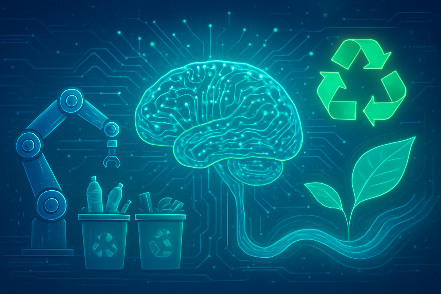
Engineering a Closed Loop: Deep Dive into Enabling Technologies
The transition to a circular economy is being propelled by a confluence of sophisticated technological advancements, spanning artificial intelligence, cutting-edge recycling methodologies, and a new generation of materials. These innovations collectively represent a paradigm shift from the linear "take-make-dispose" model, offering unprecedented capabilities for resource optimization and waste minimization.
Artificial Intelligence (AI) as the Architect of Circularity: AI is proving to be an indispensable tool, acting as the strategic mastermind behind circular operations. Its capabilities extend from optimizing resource use and waste reduction across entire supply chains to revolutionizing recycling infrastructure. AI-powered robots, equipped with advanced computer vision, are now capable of sorting diverse waste streams—plastics, paper, metals—with a precision and speed far exceeding manual methods. This technical leap is crucial, as it ensures higher quality and quantity of recovered materials, which are essential for advanced recycling processes. Furthermore, AI algorithms are enabling predictive maintenance for machinery, extending product lifecycles, and optimizing logistics to minimize waste and emissions. Unlike traditional, often static and reactive waste management approaches, AI offers a dynamic, data-driven, and systemic view, balancing economic, environmental, and social criteria. The AI research community largely views this integration as a vast, largely untapped opportunity, though challenges remain in data quality, initial investment costs, and ethical considerations.
Advanced Recycling: Beyond Mechanical Limits: While mechanical recycling remains vital, advanced recycling methods are tackling complex and contaminated waste streams that were previously unrecyclable, often destined for landfills or incineration.
- Chemical Recycling, also known as molecular recycling, breaks down plastic polymers into their molecular building blocks (monomers or intermediate chemicals) through processes like pyrolysis, gasification, and depolymerization. Pyrolysis involves heating plastics in the absence of oxygen (300-400 °C) to yield pyrolysis oil and gases, capable of processing mixed plastics into virgin-like quality feedstock. Gasification converts plastics into syngas (hydrogen and carbon monoxide) in a controlled oxygen atmosphere, which can then be used to produce methanol or other chemicals, offering high tolerance for feedstock contamination. Depolymerization (e.g., solvolysis for PET) specifically breaks down polymers into their original monomers using solvents, heat, or enzymes, allowing for infinite recycling without quality degradation, a significant advantage over the "downcycling" often associated with mechanical methods.
- Biological Recycling employs microorganisms or enzymes (like PETase and MHETase) to degrade plastics under milder conditions. This enzymatic or microbial degradation offers an environmentally gentler approach, converting polymers into reusable monomers with high selectivity. This is a stark contrast to the energy-intensive and sometimes chemical-heavy nature of other advanced recycling methods.
- Advanced Mechanical Recycling (AMR) builds on traditional methods by integrating enhanced sorting, washing, deodorization, and extrusion technologies. This allows AMR to process a wider range of post-consumer plastics, including mixed streams, into high-quality, "virgin-like" recycled pellets, addressing the quality gap that often limited the application of mechanically recycled materials.
While proponents highlight the potential of advanced recycling to create high-quality, circular plastics, environmental experts raise concerns about the energy intensity, pollution potential, and the tendency for some processes to convert plastic into fuel rather than new plastic, effectively acting as incineration.
Novel Materials: The Foundation of Future Circularity: The development of new materials is equally critical.
- Bio-based Materials, such as Polylactic Acid (PLA), Polyhydroxyalkanoates (PHA), and starch-based polymers, are derived from renewable organic sources. PLA, from fermented starches, is compostable and used in packaging, while PHA, produced by bacteria, offers properties similar to conventional plastics with biodegradability. These materials significantly reduce reliance on fossil fuels and often boast a lower carbon footprint, though their mechanical and thermal performance sometimes lags behind their fossil-based counterparts.
- Waste Valorization Materials transform industrial and agricultural wastes into valuable products. Examples include using agricultural residues (rice husk ash, sugarcane bagasse, banana leaf ash) to produce lightweight, thermally efficient construction materials like bricks and concrete, and industrial byproducts (blast furnace slag, fly ash) to replace cement in concrete, reducing CO2 emissions. This directly converts waste into resources, addressing disposal issues and reducing reliance on virgin materials.
- Metal-Organic Frameworks (MOFs) are a class of crystalline porous materials with high porosity and tunable chemical structures. They show remarkable potential for CO2 capture and conversion, gas separation, and catalysis due to their highly selective adsorption capabilities and customizable structures. While promising for energy-intensive applications, their high cost currently limits widespread industrial adoption.
These technological pillars are not isolated but interconnected, with AI optimizing the processes for advanced recycling and the integration of novel materials. The collective impact is a powerful engine driving the shift towards a truly circular economy, though careful consideration of energy consumption, environmental impacts, and economic viability remains paramount for each specific technology.
Corporate Reinvention: Navigating the Circular Economy's Impact on Industry
The integration of AI and advanced material science into circular economy principles is not merely an environmental initiative; it's a profound corporate reinvention, fundamentally altering business models, supply chains, and competitive landscapes for AI companies, tech giants, and agile startups alike. This shift promises to unlock new revenue streams, enhance brand value, and build unprecedented resilience against resource volatility.
AI companies are at the forefront of this transformation, providing the foundational technologies that make circularity scalable and intelligent. Their machine learning, computer vision, and predictive analytics capabilities are indispensable for optimizing every facet of the circular economy. From accelerating the discovery of novel sustainable materials and simulating complex chemical interactions for advanced batteries to enhancing waste sorting accuracy and optimizing reverse logistics, AI is creating entirely new market segments. Companies specializing in AI-driven material intelligence, waste management platforms, and predictive maintenance software are experiencing burgeoning demand.
Tech giants, with their vast data infrastructure and cloud computing prowess, are strategically embedding circular economy principles into their operations and product offerings. Alphabet Inc. (NASDAQ: GOOGL), through Google, is leveraging its algorithmic capabilities to help industries like fashion assess environmental impact and is actively collaborating on AI databases to advance the recycling of challenging materials like flexible plastics. Similarly, Microsoft Corp. (NASDAQ: MSFT) and International Business Machines Corp. (NYSE: IBM) are developing comprehensive solutions that integrate AI, IoT, and cloud infrastructure to optimize resource flows and reduce waste across diverse applications. These companies are also redesigning their own hardware for repairability and modularity, extending product lifecycles, and exploring "second-life" solutions to combat e-waste. Their ability to process immense datasets allows for continuous refinement of circular business models, enabling them to simulate environmental impacts and adapt to fluctuating market dynamics.
Startups are emerging as nimble disruptors, often building circularity into their core business models from inception. These agile firms are pioneering innovative solutions in areas such as AI-powered waste transformation, automated recycling, and hyper-transparent supply chains. Many are championing "product-as-a-service" (PaaS) models, lease-based offerings, and sharing economies, which are inherently circular. Examples include companies developing advanced biodegradable plastics or utilizing AI for precise sales forecasting to minimize food waste in supermarkets. Their success is often predicated on strategic partnerships with established firms and access to patient capital to scale their pilot technologies.
Companies poised to benefit significantly from this paradigm shift include TOMRA Systems ASA (OSE: TOM), a leader in sorting and collection technologies that utilizes AI and computer vision for highly efficient material recovery. Hewlett Packard Enterprise (NYSE: HPE) is driving innovation in product design for repairability and offering services that optimize resource usage. Material science giants like Dow Inc. (NYSE: DOW) are actively collaborating on AI initiatives to identify and advance the recycling of challenging materials. Even automotive innovators like Tesla, Inc. (NASDAQ: TSLA) are applying AI in their battery recycling processes to maximize component recovery and reuse. Consumer goods behemoths like Unilever PLC (NYSE: UL) are employing AI to simulate and evaluate sustainable packaging materials and optimize designs for recycled plastic utilization.
The competitive implications are profound. Companies that master the convergence of AI and circular economy principles will gain a significant edge through lower operational costs, more resilient supply chains, and enhanced customer loyalty. Conversely, those that delay adoption risk escalating costs, shrinking margins, and a loss of market share. "Born-circular" startups are expected to disrupt traditional linear businesses, mirroring the impact of "born-digital" companies on analogue models. This necessitates a collaborative ecosystem approach, transforming regulatory pressures into opportunities for value creation.
The disruption extends to existing products and services. The traditional "take-make-waste" model is rapidly becoming obsolete. Product-as-a-service models will challenge conventional ownership, requiring manufacturers to prioritize durability, maintenance, and end-of-life recovery. Planned obsolescence will give way to designs emphasizing modularity, reparability, and recyclability, particularly impacting industries with rapid product cycles like consumer electronics. Traditional waste management services will be reshaped by AI-driven advanced recycling, leading to higher material recovery rates and reduced landfill dependency. Existing linear supply chains will need to be rewired to support complex reverse logistics, remanufacturing, and dynamic material flows.
For companies to thrive, strategic market positioning is crucial. This involves leadership in circular design, leveraging AI-driven material science for durable and recyclable products, and shifting towards service-oriented business models. Deploying AI and IoT for advanced resource management, embracing transparency through blockchain-powered digital product passports, and fostering ecosystem collaboration are also key. The core impact on business models is a fundamental shift towards regenerative and resilient operations, where value creation extends beyond new sales to include product longevity and resource recovery. R&D will prioritize sustainable material development and modular design, while AI-powered analytics will become central to strategic planning, risk mitigation, and deeply integrating ESG (Environmental, Social, and Governance) strategies into the business fabric.
A Regenerative Future: The Broader Significance of Circular Innovations
The convergence of AI, advanced materials, and circular economy principles represents far more than a series of isolated technological advancements; it signifies a pivotal shift in the broader AI landscape and holds profound implications for society and the environment. By December 2025, these innovations are rapidly moving from nascent concepts to integrated solutions, aligning with a growing trend towards application-driven intelligence and systemic optimization.
This integration fits squarely within the broader AI trend of data-driven discovery and optimization. AI's capacity to process and analyze immense datasets is accelerating the identification of novel sustainable materials, moving beyond the slow, resource-intensive experimental approaches of the past. Similarly, in advanced recycling, AI is analyzing historical waste data to predict generation patterns, optimize sorting, and enhance efficiency. The rise of generative AI, a significant recent milestone, is proving crucial for designing new materials optimized for durability, reparability, and recyclability from the outset. Tools like Microsoft's MatterGen are exploring previously intractable material spaces, promising a new era of sustainable design.
The increasing sophistication of digital twins and IoT integration is also a key enabler. AI-powered virtual replicas of physical assets and processes, coupled with real-time data from IoT sensors, are creating "smart waste networks" that optimize collection, reduce fuel consumption, and enhance recycling throughout a product's lifecycle. Furthermore, automation and robotics, driven by AI and computer vision, are revolutionizing waste segregation by identifying and separating recyclable materials with unprecedented precision, reducing contamination and improving the quality of recycled outputs. This systemic integration of AI across the value chain distinguishes the current wave of innovation from earlier, more siloed AI applications.
The impacts on society and the environment are overwhelmingly positive. Environmentally, these innovations promise drastic waste reduction and resource efficiency by optimizing everything from waste collection to material sorting, thereby minimizing reliance on virgin resources. AI accelerates the discovery of eco-friendly materials like bio-based polymers and low-carbon cements, leading to greener industries and reduced pollution. By optimizing production, extending product lifespans, and enhancing recycling, AI contributes significantly to a lower carbon footprint. Socially and economically, this transition fosters economic growth through new business models like Product-as-a-Service (PaaS), which keeps products in circulation longer, creating value from recovered materials. It also contributes to improved quality of life through cleaner cities and provides enhanced decision-making capabilities for policymakers and businesses.
However, this transformative potential is accompanied by several potential concerns. The efficacy of AI models depends heavily on data quality and the risk of bias, with data scarcity in material science posing a significant bottleneck. There's also the critical issue of the environmental footprint of AI itself; the energy and computational resources required for large AI models could potentially offset the efficiency gains in circularity, and the demand for advanced hardware might exacerbate electronic waste. Ethical implications around fairness, transparency, and accountability in AI decision-making are paramount, as is data privacy when collecting vast amounts of environmental and social data. Concerns about job displacement in traditional industries and the risk of greenwashing (where AI is used to make unsustainable practices appear marginally greener without fundamental change) also need careful consideration.
Comparing this wave of AI innovation to previous milestones reveals a significant evolution. Unlike earlier rule-based AI systems, modern AI leverages vast datasets to learn complex patterns and generate novel solutions, as seen in advanced material discovery and precision recycling. This marks a shift from incremental improvements to accelerated discovery, reducing material development cycles from years to weeks. Crucially, the current trend emphasizes integration and systemic optimization across entire value chains, going beyond localized efficiencies to a holistic approach to resource management. This represents a maturing of AI capabilities from theoretical potential to tangible, impactful applications, enabling a level of efficiency, precision, and innovation in sustainability and material science that was previously unattainable. The circular economy, powered by AI, is not just a trend but a fundamental re-architecture of our industrial and consumption systems.
The Horizon of Circularity: Future Developments and Expert Predictions
The integration of AI, advanced materials, and circular economy principles is not a static phenomenon; it is a rapidly evolving frontier with transformative near-term and long-term developments on the horizon. Experts predict that by 2030, AI will be a foundational element across industries, driving unprecedented efficiency, innovation, and systemic change.
In the near term (2025-2028), we can expect significant advancements in several key areas. Smarter waste management and recycling will see AI-powered systems, leveraging image recognition and robotics, revolutionize sorting speed and accuracy, particularly for complex, multi-material products. This will drastically reduce contamination and improve the quality of recycled outputs. Predictive maintenance, driven by AI algorithms analyzing sensor data, will extend product lifespans by an estimated 40-60%, reducing waste and maintenance costs. Enhanced supply chain transparency and optimization will see AI provide real-time insights into material flows, tracing origins, monitoring environmental impact, and optimizing logistics to reduce overproduction. AI-assisted circular product design tools will become more sophisticated, helping businesses create products inherently easier to repair, upgrade, and recycle by analyzing vast datasets on material performance and supply chain logistics. The acceleration of sustainable material discovery through AI-driven material informatics will lead to faster development of self-healing polymers, biodegradable materials, and low-carbon construction alternatives. Furthermore, AI will continue to bolster Product-as-a-Service (PaaS) models by tracking usage and optimizing maintenance, while personalized consumer engagement through AI-powered apps will guide individuals towards more sustainable choices.
Looking into the long term (beyond 2028), AI's role is expected to become even more pervasive and transformative. We may see the advent of programmable materials that can dynamically change properties based on environmental conditions, enhancing adaptability and reusability. AI could also be applied to the complex task of system-level redesign, rewiring global supply chains and optimizing reverse logistics infrastructure across entire sectors to achieve true circularity. The convergence of AI and blockchain technology will lead to robust digital product passports, ensuring unprecedented transparency and traceability from raw material to end-of-life. More sophisticated generative eco-design will enable engineers to create novel product designs that inherently minimize material usage and are optimized for disassembly and reuse. Experts predict AI will transition from merely supporting decision-making to becoming an active decision-making co-pilot, dynamically adjusting energy grids, forecasting climate risks, and autonomously redesigning business processes. The emergence of Circular Economy as a Service (CEaaS) platforms, powered by AI, will democratize access to circular practices for companies lacking internal expertise.
Potential applications and use cases are expanding across diverse industries. In waste management, autonomous AI robots will revolutionize e-waste disassembly, accurately recovering valuable rare earth elements. In manufacturing, AI will optimize material usage and facilitate dynamic process adjustments to incorporate eco-friendly materials. Construction will see AI design low-carbon concrete mixes and track materials throughout their lifecycle, contributing to a "circular construction" model. In food and agriculture, AI will optimize harvest times and match supply and demand to reduce spoilage. In retail and fashion, AI will predict demand to prevent overproduction, while smart tags and AI-powered platforms will optimize resale and rental services.
However, several challenges must be addressed. Data fragmentation and quality remain significant hurdles, as AI thrives on vast, consistent datasets that are often lacking in complex supply chains. The economic costs and investment required for AI implementation and infrastructure can be a barrier, particularly for SMEs. The energy consumption of AI itself, especially large models, must be carefully managed to ensure its environmental benefits are not negated by its own footprint. Ethical concerns around data privacy, algorithmic bias, and the need for transparent AI decision-making are paramount. A lack of comprehensive regulatory frameworks could hinder responsible deployment, and ensuring the performance and longevity of new AI-designed materials to match traditional counterparts remains a challenge. Finally, significant infrastructure gaps for reverse logistics and material processing need to be overcome.
Despite these challenges, expert predictions are overwhelmingly optimistic. AI is expected to become a core business driver by 2026, central to predictive demand planning, energy optimization, and smart reverse logistics. Research and development in AI for the circular economy have seen a dramatic increase, indicating a growing recognition of its value. AI-driven material informatics will continue to accelerate breakthroughs in inherently circular and non-toxic materials. By 2030, mastering "circular intelligence" – the convergence of AI and circular economy principles – will be a prerequisite for competitiveness, with AI becoming the foundation for real-time decision-making. The economic opportunities are projected to reach hundreds of billions, potentially trillions, of dollars annually by 2030, driven by AI's ability to design out waste in critical sectors. The continued convergence of AI with other Industry 4.0 technologies like IoT, blockchain, and advanced robotics will create increasingly efficient, transparent, and resilient circular systems. The future envisions AI as an indispensable catalyst for a regenerative, resilient, and resource-efficient global economy.
The Dawn of a Regenerative Era: A Concluding Outlook
The fusion of AI with advancements in sustainability and material science marks a pivotal moment in both technological evolution and environmental stewardship. The journey towards a truly circular economy, once a distant ideal, is now being rapidly accelerated by intelligent systems and innovative materials.
Key Takeaways: The core message is one of unprecedented efficiency and innovation. AI dramatically accelerates the discovery, design, and recycling processes, slashing timelines from years to mere weeks. It drastically improves the accuracy and quality of material identification and sorting, reducing contamination and elevating the purity of recycled outputs. This leads to data-driven decision-making across the entire value chain, from predicting material behavior to optimizing supply chain flows. Crucially, generative AI is unlocking entirely new possibilities, creating novel materials and reaction pathways tailored for sustainable applications. Ultimately, these advancements are directly contributing to a significant reduction in waste and virgin resource consumption, lowering carbon emissions, and fostering a more sustainable industrial ecosystem.
Significance in AI History: This application of AI represents a profound leap, moving beyond theoretical advancements to tangible, real-world industrial impact that addresses some of humanity's most pressing challenges. AI's ability to analyze vast datasets, simulate complex interactions, and generate novel solutions far surpasses human capacity, ushering in an era of "self-driving materials science." This domain unequivocally showcases AI's potential as a powerful tool for global good, contributing directly to environmental stewardship and the UN Sustainable Development Goals. It also highlights the growing sophistication of AI in automating complex physical processes, from laboratory experimentation to industrial recycling, fundamentally transforming the entire discovery process in materials science.
Long-Term Impact: The long-term impact is poised to be transformative, driving a paradigm shift towards a "renewable carbon economy" and a vision of "full circularity" where bio-based, CO2-based, and recycled materials replace fossil resources, maintaining carbon in closed loops. This will lead to more resilient economies, less vulnerable to resource scarcity and price fluctuations. AI will optimize sustainable infrastructure, including reverse logistics, advanced remanufacturing, and "circular construction," ensuring materials retain their highest utility and value. Furthermore, AI will enable personalized product design, fostering stronger consumer attachment and longer product lifespans. The scalability offered by AI is poised to move circular economy initiatives from niche practices to mainstream industrial standards.
What to Watch For in the Coming Weeks and Months (Considering 12/9/2025): As we close out 2025, the momentum in this space is undeniable. Keep a close eye on further developments in generative AI for advanced materials, with new announcements expected from platforms like MatterGen and industry innovators. The scaling and refinement of AI-supported chemical recycling technologies for plastics will be crucial. Expect continuous improvements in deep learning algorithms for waste sorting, leading to even higher accuracy in identifying complex and previously unrecyclable materials. The expansion of digital twin technology in recycling facilities for real-time monitoring and process optimization will be a significant trend. Finally, watch for increased efforts in standardization and collaboration across the circular economy value chain, as well as insights emerging from key events like the upcoming AI Circular Economy Conference in March 2026, which promises to highlight cutting-edge presentations on AI's role in circularity. The coming months will undoubtedly solidify AI's position as an indispensable catalyst for a greener, more resilient global economy.
This content is intended for informational purposes only and represents analysis of current AI developments.
TokenRing AI delivers enterprise-grade solutions for multi-agent AI workflow orchestration, AI-powered development tools, and seamless remote collaboration platforms.
For more information, visit https://www.tokenring.ai/.