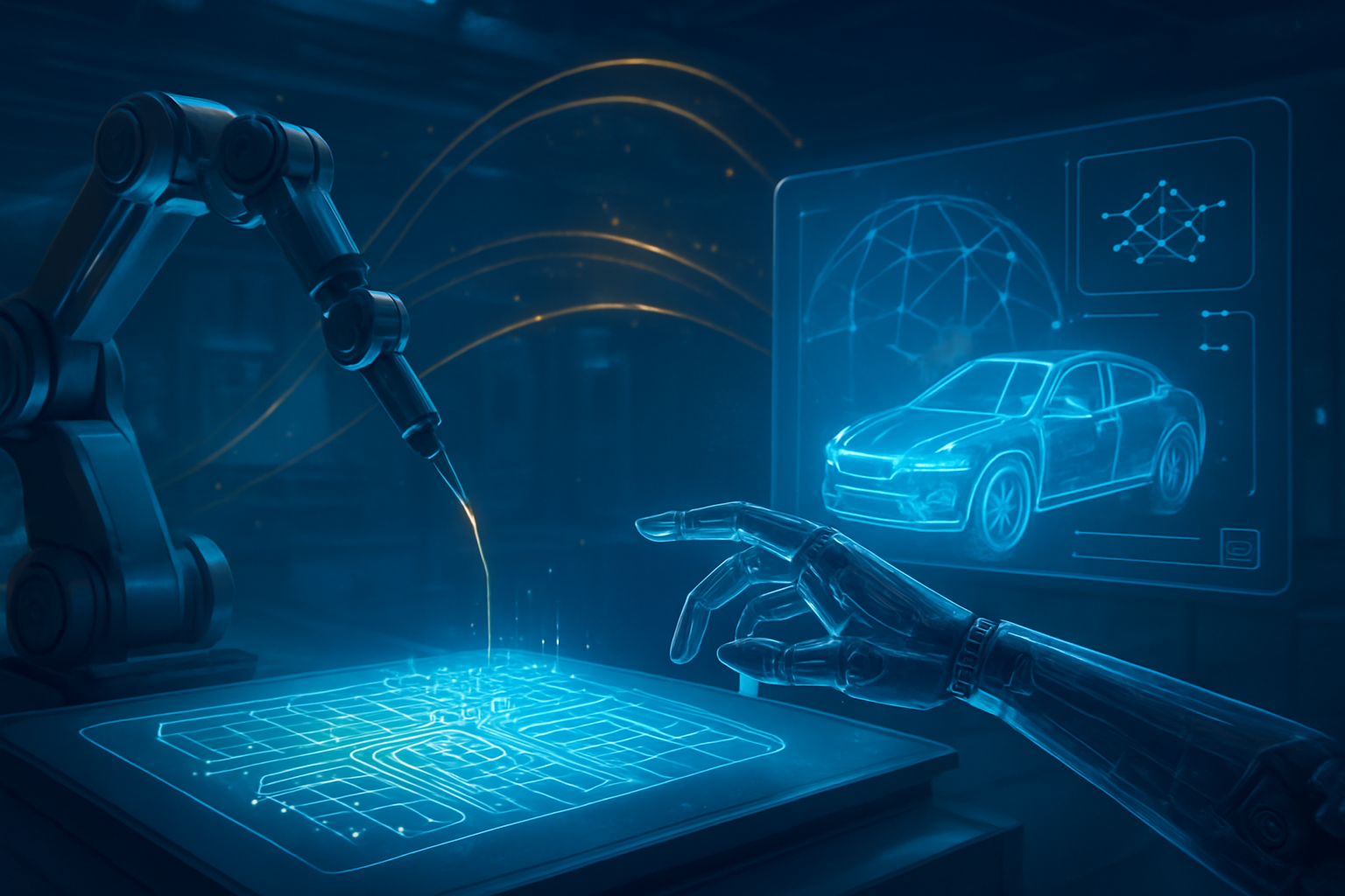
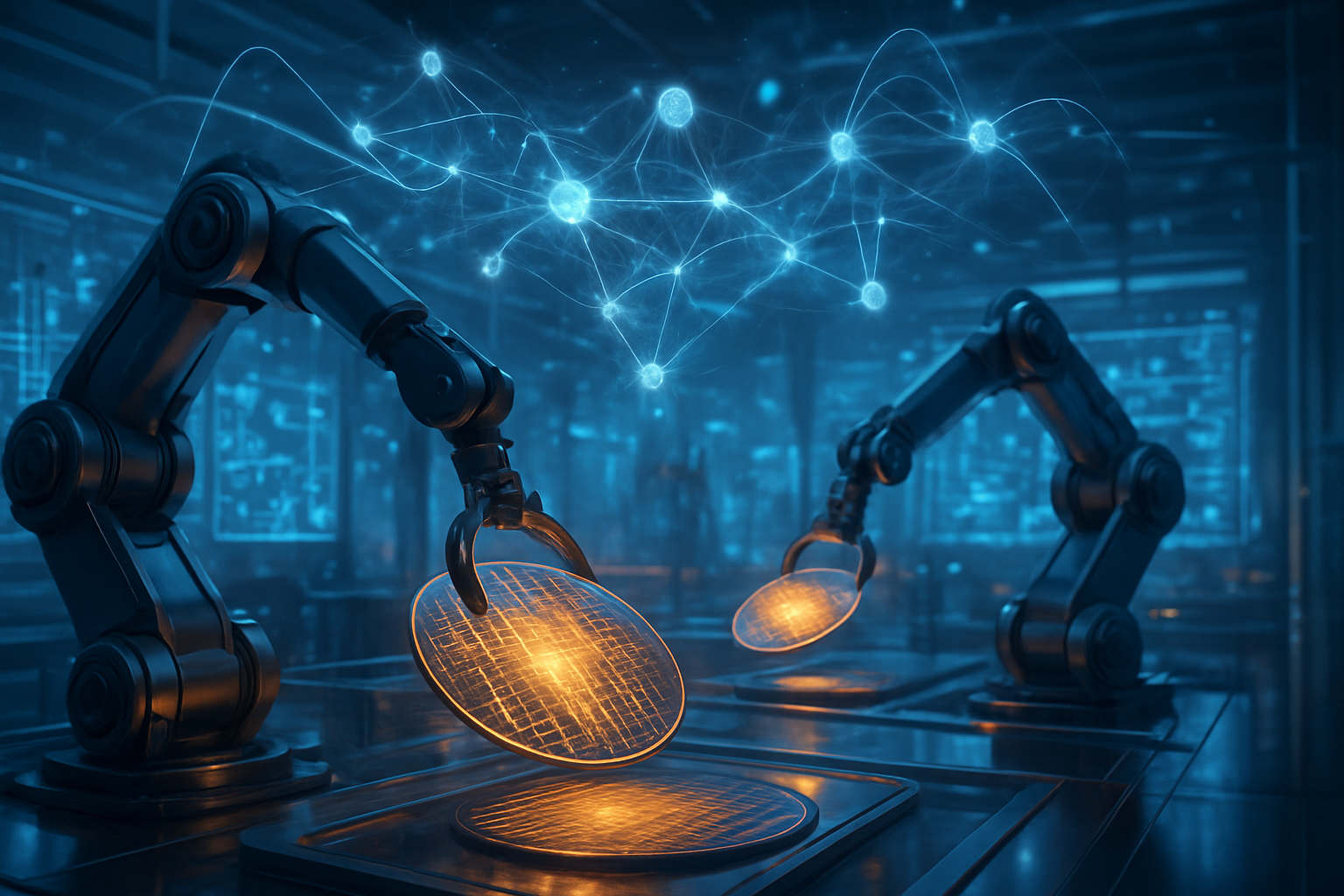
Tag: Synopsys

  • The Architect Within: How AI-Driven Design is Accelerating the Next Generation of Silicon

    The Architect Within: How AI-Driven Design is Accelerating the Next Generation of Silicon

    In a profound shift for the semiconductor industry, the boundary between hardware and software has effectively dissolved as artificial intelligence (AI) takes over the role of the master architect. This transition, led by breakthroughs from Alphabet Inc. (NASDAQ:GOOGL) and Synopsys, Inc. (NASDAQ:SNPS), has turned a process that once took human engineers months of painstaking effort into a task that can be completed in a matter of hours. By treating chip layout as a complex game of strategy, reinforcement learning (RL) is now designing the very substrates upon which the next generation of AI will run.

    This "AI-for-AI" loop is not just a laboratory curiosity; it is the new production standard. In early 2026, the industry is witnessing the widespread adoption of autonomous design systems that optimize for power, performance, and area (PPA) with a level of precision that exceeds human capability. The implications are staggering: as AI chips become faster and more efficient, they provide the computational power to train even more capable AI designers, creating a self-reinforcing cycle of exponential hardware advancement.

    The Silicon Game: Reinforcement Learning at the Edge

    At the heart of this revolution is the automation of "floorplanning," the incredibly complex task of arranging millions of transistors and large blocks of memory (macros) on a silicon die. Traditionally, this was a manual process involving hundreds of iterations over several months. Google DeepMind’s AlphaChip changed the paradigm by framing floorplanning as a sequential decision-making game, similar to Go or Chess. Using a custom Edge-Based Graph Neural Network (Edge-GNN), AlphaChip learns the intricate relationships between circuit components, predicting how a specific placement will impact final wire length and signal timing.

    The results have redefined expectations for hardware development cycles. AlphaChip can now generate a tapeout-ready floorplan in under six hours—a feat that previously required a team of senior engineers working for weeks. This technology was instrumental in the rapid deployment of Google’s TPU v5 and the recently released TPU v6 (Trillium). By optimizing macro placement, AlphaChip contributed to a reported 67% increase in energy efficiency for the Trillium architecture, allowing Google to scale its AI services while managing the mounting energy demands of large language models.

    Meanwhile, Synopsys DSO.ai (Design Space Optimization) has taken a broader approach by automating the entire "RTL-to-GDSII" flow—the journey from logical design to physical layout. DSO.ai searches through an astronomical design space—estimated at $10^{90,000}$ possible permutations—to find the optimal "design recipe." This multi-objective reinforcement learning system learns from every iteration, narrowing down parameters to hit specific performance targets. As of early 2026, Synopsys has recorded over 300 successful commercial tapeouts using this technology, with partners like SK Hynix (KRX:000660) reporting design cycle reductions from weeks to just three or four days.

    The Strategic Moat: The Rise of the 'Virtuous Cycle'

    The shift to AI-driven design is restructuring the competitive landscape of the tech world. NVIDIA Corporation (NASDAQ:NVDA) has emerged as a primary beneficiary of this trend, utilizing its own massive supercomputing clusters to run thousands of parallel AI design simulations. This "virtuous cycle"—using current-generation GPUs to design future architectures like the Blackwell and Rubin series—has allowed NVIDIA to compress its product roadmap, moving from a biennial release schedule to a frantic annual pace. This speed creates a significant barrier to entry for competitors who lack the massive compute resources required to run large-scale design space explorations.

    For Electronic Design Automation (EDA) giants like Synopsys and Cadence Design Systems, Inc. (NASDAQ:CDNS), the transition has turned their software into "agentic" systems. Cadence's Cerebrus tool now offers a "10x productivity gain," enabling a single engineer to manage the design of an entire System-on-Chip (SoC) rather than just a single block. This effectively grants established chipmakers the ability to achieve performance gains equivalent to a full "node jump" (e.g., from 5nm to 3nm) purely through software optimization, bypassing some of the physical limitations of traditional lithography.

    Furthermore, this technology is democratizing custom silicon for startups. Previously, only companies with billion-dollar R&D budgets could afford the specialized teams required for advanced chip design. Today, startups are using AI-powered tools and "Natural Language Design" interfaces—similar to Chip-GPT—to describe hardware behavior in plain English and generate the underlying Verilog code. This is leading to an explosion of "bespoke" silicon tailored for specific tasks, from automotive edge computing to specialized biotech processors.

    Breaking the Compute Bottleneck and Moore’s Law

    The significance of AI-driven chip design extends far beyond corporate balance sheets; it is arguably the primary force keeping Moore’s Law on life support. As physical transistors approach the atomic scale, the gains from traditional shrinking have slowed. AI-driven optimization provides a "software-defined" boost to efficiency, squeezing more performance out of existing silicon footprints. This is critical as the industry faces a "compute bottleneck," where the demand for AI training cycles is outstripping the supply of high-performance hardware.

    However, this transition is not without its concerns. The primary challenge is the "compute divide": a single design space exploration run can cost tens of thousands of dollars in cloud computing fees, potentially concentrating power in the hands of the few companies that own large-scale GPU farms. Additionally, there are growing anxieties within the engineering community regarding job displacement. As routine physical design tasks like routing and verification become fully automated, the role of the Very Large Scale Integration (VLSI) engineer is shifting from manual layout to high-level system orchestration and AI model tuning.

    Experts also point to the environmental implications. While AI-designed chips are more energy-efficient once they are running in data centers, the process of designing them requires immense amounts of power. Balancing the "carbon cost of design" against the "carbon savings of operation" is becoming a key metric for sustainability-focused tech firms in 2026.

    The Future: Toward 'Lights-Out' Silicon Factories

    Looking toward the end of the decade, the industry is moving from AI-assisted design to fully autonomous "lights-out" chipmaking. By 2028, experts predict the first major chip projects will be handled entirely by swarms of specialized AI agents, from initial architectural specification to the final file sent to the foundry. We are also seeing the emergence of AI tools specifically for 3D Integrated Circuits (3D-IC), where chips are stacked vertically. These designs are too complex for human intuition, involving thousands of thermal and signal-integrity variables that only a machine learning model can navigate effectively.

    Another horizon is the integration of AI design with "lights-out" manufacturing. Plants like Xiaomi’s AI-native facilities are already demonstrating 100% automation in assembly. The next step is a real-time feedback loop where the design software automatically adjusts the chip layout based on the current capacity and defect rates of the fabrication plant, creating a truly fluid and adaptive supply chain.

    A New Era of Hardware

    The era of the "manual" chip designer is drawing to a close, replaced by a symbiotic relationship where humans set the high-level goals and AI explores the millions of ways to achieve them. The success of AlphaChip and DSO.ai marks a turning point in technological history: for the first time, the tools we have created are designing the very "brains" that will allow them to surpass us.

    As we move through 2026, the industry will be watching for the first fully "AI-native" architectures—chips that look nothing like what a human would design, featuring non-linear layouts and unconventional structures optimized solely by the cold logic of an RL agent. The silicon revolution has only just begun, and the architect of its future is the machine itself.


    This content is intended for informational purposes only and represents analysis of current AI developments.

    TokenRing AI delivers enterprise-grade solutions for multi-agent AI workflow orchestration, AI-powered development tools, and seamless remote collaboration platforms.
    For more information, visit https://www.tokenring.ai/.

  • The Silicon Renaissance: How AI-Led EDA Tools are Redefining Chip Design at CES 2026

    The Silicon Renaissance: How AI-Led EDA Tools are Redefining Chip Design at CES 2026

    The traditional boundaries of semiconductor engineering were shattered this month at CES 2026, as the industry pivoted from human-centric chip design to a new era of "AI-defined" hardware. Leading the charge, Electronic Design Automation (EDA) giants demonstrated that the integration of generative AI and reinforcement learning into the silicon lifecycle is no longer a luxury but a fundamental necessity for survival. By automating the most complex phases of design, these tools are now delivering the impossible: reducing development timelines from months to mere weeks while slashing prototyping costs by 20% to 60%.

    The significance of this shift cannot be overstated. As the physical limits of Moore’s Law loom, the industry has found a new tailwind in software intelligence. The transformation is particularly visible in the automotive and high-performance computing sectors, where the need for bespoke, AI-optimized silicon has outpaced the capacity of human engineering teams. With the debut of new virtualized ecosystems and "agentic" design assistants, the barriers to entry for custom silicon are falling, ushering in a "Silicon Renaissance" that promises to accelerate innovation across every vertical of the global economy.

    The Technical Edge: Arm Zena and the Virtualization Revolution

    At the heart of the announcements at CES 2026 was the deep integration between Synopsys (Nasdaq: SNPS) and Arm (Nasdaq: ARM). Synopsys unveiled its latest Virtualizer Development Kits (VDKs) specifically optimized for the Arm Zena Compute Subsystem (CSS). The Zena CSS is a marvel of modular engineering, featuring a 16-core Arm Cortex-A720AE cluster and a dedicated "Safety Island" for real-time diagnostics. By using Synopsys VDKs, automotive engineers can now create a digital twin of the Zena hardware. This allows software teams to begin writing and testing code for next-generation autonomous driving features up to a year before the actual physical silicon returns from the foundry—a practice known as "shifting left."

    Meanwhile, Cadence Design Systems (Nasdaq: CDNS) showcased its own breakthroughs in engineering virtualization through the Helium Virtual and Hybrid Studio. Cadence's approach focuses on "Physical AI," where chiplet-based designs are validated within a virtual environment that mirrors the exact performance characteristics of the target hardware. Their partner ecosystem, which includes Samsung Electronics (OTC: SSNLF) and Arteris (Nasdaq: AIPRT), demonstrated how pre-validated chiplets could be assembled like Lego blocks. This modularity, combined with Cadence’s Cerebrus AI, allows for the autonomous optimization of "Power, Performance, and Area" (PPA), evaluating $10^{90,000}$ design permutations to find the most efficient layout in a fraction of the time previously required.

    The most startling technical metric shared during the summit was the impact of Generative AI on floorplanning—the process of arranging circuits on a silicon die. What used to be a grueling, multi-month iterative process for teams of senior engineers is now being handled by AI agents like Synopsys.ai Copilot. These agents analyze historical design data and real-time constraints to produce optimized layouts in days. The resulting 20-60% reduction in costs stems from fewer "respins" (expensive design corrections) and a significantly reduced need for massive, specialized engineering cohorts for routine optimization tasks.

    Competitive Landscapes and the Rise of the Hyperscalers

    The democratization of high-end chip design through AI-led EDA tools is fundamentally altering the competitive landscape. Traditionally, only giants like Nvidia (Nasdaq: NVDA) or Apple (Nasdaq: AAPL) had the resources to design world-class custom silicon. Today, the 20-60% cost reduction and timeline compression mean that mid-tier automotive OEMs and startups can realistically pursue custom SoCs (System on Chips). This shifts the power dynamic away from general-purpose chip makers and toward those who can design specific hardware for specific AI workloads.

    Cloud providers are among the biggest beneficiaries of this shift. Amazon (Nasdaq: AMZN) and Microsoft (Nasdaq: MSFT) are already leveraging these AI-driven tools to accelerate their internal silicon roadmaps, such as the Graviton and Maia series. By utilizing the "ISA parity" offered by the Arm Zena ecosystem, these hyperscalers can provide developers with a seamless environment where code written in the cloud runs identically on edge devices. This creates a feedback loop that strengthens the grip of cloud giants on the AI development pipeline, as they now provide both the software tools and the optimized hardware blueprints.

    Foundries and specialized chip makers are also repositioning themselves. NXP Semiconductors (Nasdaq: NXPI) and Texas Instruments (Nasdaq: TXN) have integrated Synopsys VDKs into their workflows to better serve the "Software-Defined Vehicle" (SDV) market. By providing virtual models of their upcoming chips, they lock in automotive manufacturers earlier in the design cycle. This creates a "virtual-first" sales model where the software environment is as much a product as the physical silicon, making it increasingly difficult for legacy players who lack a robust AI-EDA strategy to compete.

    Beyond the Die: The Global Significance of AI-Led EDA

    The transformation of chip design carries weight far beyond the technical community; it is a geopolitical and economic milestone. As nations race for "chip sovereignty," the ability to design high-performance silicon locally—without a decades-long heritage of manual engineering expertise—is a game changer. AI-led EDA tools act as a "force multiplier," allowing smaller nations and regional hubs to establish viable semiconductor design sectors. This could lead to a more decentralized global supply chain, reducing the world's over-reliance on a handful of design houses in Silicon Valley.

    However, this rapid advancement is not without its concerns. The automation of complex engineering tasks raises questions about the future of the semiconductor workforce. While the industry currently faces a talent shortage, the transition from months to weeks in design cycles suggests that the role of the "human-in-the-loop" is shifting toward high-level architectural oversight rather than hands-on optimization. There is also the "black box" problem: as AI agents generate increasingly complex layouts, ensuring the security and verifiability of these designs becomes a paramount challenge for mission-critical applications like aerospace and healthcare.

    Comparatively, this breakthrough mirrors the transition from assembly language to high-level programming in the 1970s. Just as compilers allowed software to scale exponentially, AI-led EDA is providing the "silicon compiler" that the industry has sought for decades. It marks the end of the "hand-crafted" era of chips and the beginning of a generative era where hardware can evolve as rapidly as the software that runs upon it.

    The Horizon: Agentic EDA and Autonomous Foundries

    Looking ahead, the next frontier is "Agentic EDA," where AI systems do not just assist engineers but proactively manage the entire design-to-manufacturing pipeline. Experts predict that by 2028, we will see the first "lights-out" chip design projects, where the entire process—from architectural specification to GDSII (the final layout file for the foundry)—is handled by a swarm of specialized AI agents. These agents will be capable of real-time negotiation with foundry capacity, automatically adjusting designs based on available manufacturing nodes and material costs.

    We are also on the cusp of seeing AI-led design move into more exotic territories, such as photonic and quantum computing chips. The complexity of routing light or managing qubits is a perfect use case for the reinforcement learning models currently being perfected for silicon. As these tools mature, they will likely be integrated into broader industrial metaverses, where a car's entire electrical architecture, chassis, and software are co-optimized by a single, unified AI orchestrator.

    A New Era for Innovation

    The announcements from Synopsys, Cadence, and Arm at CES 2026 have cemented AI's role as the primary architect of the digital future. The ability to condense months of work into weeks and slash costs by up to 60% represents a permanent shift in how humanity builds technology. This "Silicon Renaissance" ensures that the explosion of AI software will be met with a corresponding leap in hardware efficiency, preventing a "compute ceiling" from stalling progress.

    As we move through 2026, the industry will be watching the first production vehicles and servers born from these virtualized AI workflows. The success of the Arm Zena CSS and the widespread adoption of Synopsys and Cadence’s generative tools will serve as the benchmark for the next decade of engineering. The hardware world is finally moving at the speed of software, and the implications for the future of artificial intelligence are limitless.


    This content is intended for informational purposes only and represents analysis of current AI developments.

    TokenRing AI delivers enterprise-grade solutions for multi-agent AI workflow orchestration, AI-powered development tools, and seamless remote collaboration platforms.
    For more information, visit https://www.tokenring.ai/.

  • The Silicon Renaissance: How Generative AI Matured to Master the 2nm Frontier in 2026

    The Silicon Renaissance: How Generative AI Matured to Master the 2nm Frontier in 2026

    As of January 2026, the semiconductor industry has officially crossed a Rubicon that many thought would take decades to reach: the full maturity of AI-driven chip design. The era of manual "trial and error" in transistor layout has effectively ended, replaced by an autonomous, generative design paradigm that has made the mass production of 2nm process nodes not only possible but commercially viable. Leading the charge are Electronic Design Automation (EDA) titans Synopsys (NASDAQ: SNPS) and Cadence Design Systems (NASDAQ: CDNS), which have successfully transitioned from providing "AI-assisted" tools to deploying fully "agentic" AI systems that reason, plan, and execute complex chip architectures with minimal human intervention.

    This transition marks a pivotal moment for the global tech economy. In early 2026, the integration of generative AI into EDA workflows has slashed design cycles for flagship processors from years to months. With the 2nm node introducing radical physical complexities—such as Gate-All-Around (GAA) transistors and Backside Power Delivery Networks (BSPDN)—the sheer mathematical density of modern chips had reached a "complexity wall." Without the generative breakthroughs seen this year, the industry likely would have faced a multi-year stagnation in Moore’s Law; instead, AI has unlocked a new trajectory of performance and energy efficiency.

    Autonomous Agents and Generative Migration: The Technical Breakthroughs

    The technical centerpiece of 2026 is the emergence of "Agentic Design." Synopsys (NASDAQ: SNPS) recently unveiled AgentEngineer™, a flagship advancement within its Synopsys.ai suite. Unlike previous generative AI that merely suggested code snippets, AgentEngineer utilizes autonomous AI agents capable of high-level reasoning. These agents can independently handle "high-toil" tasks such as complex Design Rule Checking (DRC) and layout optimization for the ultra-sensitive 2nm GAA architectures. By simulating billions of layout permutations in a fraction of the time required by human engineers, Synopsys reports that these tools can compress 2nm development cycles by an estimated 12 months, effectively allowing a three-year R&D roadmap to be completed in just two.

    Simultaneously, Cadence Design Systems (NASDAQ: CDNS) has revolutionized the industry with its JedAI (Joint Enterprise Data and AI) platform and its generative node-to-node migration tools. In the 2026 landscape, a major bottleneck for chip designers was moving legacy 5nm or 3nm intellectual property (IP) to the new 2nm and A16 (1.6nm) nodes. Cadence's generative AI now allows for the automatic migration of these designs while preserving performance integrity, reducing the time required for such transitions by up to 4x. This is further bolstered by their reinforcement-learning engine, Cerebrus, which Samsung (OTC: SSNLF) recently credited with achieving a 22% power reduction on its latest 2nm-class AI accelerators.

    The technical specifications of these systems are staggering. The 2026 versions of these EDA tools now incorporate "Multiphysics AI" through integrations like the Synopsys-Ansys (NASDAQ: ANSS) merger, allowing for real-time analysis of heat, stress, and electromagnetic interference as the AI draws the chip. This holistic approach is critical for the 3D-stacked chips that have become standard in 2026, where traditional 2D routing no longer suffices. The AI doesn't just place transistors; it predicts how they will warp under thermal load before a single atom of silicon is ever etched.

    The Competitive Landscape: Winners in the 2nm Arms Race

    The primary beneficiaries of this AI maturity are the major foundries and the hyperscale "fabless" giants. TSMC (NYSE: TSM), Samsung, and Intel (NASDAQ: INTC) have all integrated these AI-agentic flows into their reference designs for 2026. For tech giants like Nvidia (NASDAQ: NVDA), Apple (NASDAQ: AAPL), and Advanced Micro Devices (NASDAQ: AMD), the ability to iterate on 2nm designs every six months rather than every two years has fundamentally altered their product release cadences. We are now seeing a shift toward more specialized, application-specific silicon (ASICs) because the cost and time of designing a custom chip have plummeted thanks to AI automation.

    The competitive implications are stark. Smaller startups that previously could not afford the multi-hundred-million-dollar design costs associated with leading-edge nodes are now finding a foothold. AI-driven EDA tools have effectively democratized high-end silicon design, allowing a lean team of engineers to produce chips that would have required a thousand-person department in 2022. This disruption is forcing traditional semiconductor giants to pivot toward "AI-first" internal workflows to maintain their strategic advantage.

    Furthermore, the rise of Japan’s Rapidus—which in 2026 is using specialized AI-agentic design solutions to bypass legacy manufacturing hurdles—highlights how AI is redrawing the geopolitical map of silicon. By leveraging the automated DRC fixing and PPA (Power, Performance, Area) prediction tools provided by the Big Two EDA firms, Rapidus has managed to enter the 2nm market with unprecedented speed, challenging the traditional hegemony of East Asian foundries.

    Wider Significance: Extending Moore’s Law into the AI Era

    The broader significance of AI-driven chip design cannot be overstated. We are witnessing the first instance of "Recursive AI Improvement," where AI systems are being used to design the very hardware (GPUs and TPUs) that will train the next generation of AI. This creates a virtuous cycle: better AI leads to better chips, which in turn lead to even more powerful AI. This milestone is being compared to the transition from manual drafting to CAD in the 1980s, though the scale and speed of the current transformation are exponentially greater.

    However, this transition is not without its concerns. The automation of chip design raises questions about the long-term role of human electrical engineers. While productivity has surged by 35% in verification workflows, the industry is seeing a shift in the workforce toward "prompt engineering" for silicon and higher-level system architecture, rather than low-level transistor routing. There is also the potential for "black box" designs—chips created by AI that are so complex and optimized that human engineers may struggle to debug or reverse-engineer them in the event of a systemic failure.

    Geopolitically, the mastery of 2nm design through AI has become a matter of national security. As these tools become more powerful, access to high-end EDA software from Synopsys and Cadence is as strictly controlled as the physical lithography machines from ASML (NASDAQ: ASML). The ability to "self-design" high-efficiency silicon is now the benchmark for a nation's technological sovereignty in 2026.

    Looking Ahead: The Path to 1.4nm and Self-Correcting Silicon

    Looking toward the late 2020s, the next frontier is already visible: the 1.4nm (A14) node and the concept of "Self-Correcting Silicon." Experts predict that within the next 24 months, EDA tools will evolve from designing chips to monitoring them in real-time. We are seeing the first prototypes of chips that contain "AI Monitors" designed by Synopsys.ai, which can dynamically adjust clock speeds and voltages based on AI-predicted aging of the transistors, extending the lifespan of data center hardware.

    The challenges remaining are significant, particularly in the realm of data privacy. As EDA tools become more cloud-integrated and AI-driven, foundries and chip designers must find ways to train their generative models without exposing sensitive proprietary IP. In the near term, we expect to see the rise of "Federated Learning" for EDA, where companies can benefit from shared AI insights without ever sharing their actual chip designs.

    Summary and Final Thoughts

    The maturity of AI-driven chip design in early 2026 represents a landmark achievement in the history of technology. By integrating generative AI and autonomous agents into the heart of the design process, Synopsys and Cadence have effectively bridged the gap between the physical limits of silicon and the increasing demands of the AI era. The successful deployment of 2nm chips with GAA and Backside Power Delivery stands as a testament to the power of AI to solve the world’s most complex engineering challenges.

    As we move forward, the focus will shift from how we design chips to what we can do with the nearly infinite compute power they provide. The "Silicon Renaissance" is well underway, and in the coming weeks and months, all eyes will be on the first consumer devices powered by these AI-perfected 2nm processors. The world is about to see just how fast silicon can move when it has an AI at the drafting table.


    This content is intended for informational purposes only and represents analysis of current AI developments.

    TokenRing AI delivers enterprise-grade solutions for multi-agent AI workflow orchestration, AI-powered development tools, and seamless remote collaboration platforms.
    For more information, visit https://www.tokenring.ai/.

  • The “Silicon-to-Systems” Era Begins: Synopsys Finalizes $35 Billion Acquisition of Ansys

    The “Silicon-to-Systems” Era Begins: Synopsys Finalizes $35 Billion Acquisition of Ansys

    The landscape of semiconductor engineering has undergone a tectonic shift as Synopsys Inc. (NASDAQ: SNPS) officially completed its $35 billion acquisition of Ansys Inc., marking the largest merger in the history of electronic design automation (EDA). Finalized following a grueling 18-month regulatory review that spanned three continents, the deal represents a definitive pivot from traditional chip-centric design to a holistic "Silicon-to-Systems" philosophy. By uniting the world’s leading chip design software with the gold standard in physics-based simulation, the combined entity aims to solve the physics-defying challenges of the AI era, where heat, stress, and electromagnetic interference are now as critical to success as logic gates.

    The immediate significance of this merger lies in its timing. As of early 2026, the industry is racing toward the "Angstrom Era," with 2nm and 1.8A nodes entering mass production at foundries like Taiwan Semiconductor Manufacturing Company (NYSE: TSM) and Intel (NASDAQ: INTC). At these scales, the physical environment surrounding a chip is no longer a peripheral concern but a primary failure mode. The Synopsys-Ansys integration provides the first unified platform capable of simulating how a billion-transistor processor interacts with its package, its cooling system, and the electromagnetic noise of a modern AI data center—all before a single physical prototype is ever manufactured.

    A Unified Architecture for the Angstrom Era

    The technical backbone of the merger is the deep integration of Ansys’s multiphysics solvers directly into the Synopsys design stack. Historically, chip design and physics simulation were siloed workflows; a designer would layout a chip in Synopsys tools and then "hand off" the design to a simulation team using Ansys to check for thermal or structural issues. This sequential process often led to "late-stage surprises" where heat hotspots or mechanical warpage forced engineers back to the drawing board, costing millions in lost time. The new "Shift-Left" workflow eliminates this friction by embedding tools like Ansys RedHawk-SC and HFSS directly into the Synopsys 3DIC Compiler, allowing for real-time, physics-aware design.

    This convergence is particularly vital for the rise of multi-die systems and 3D-ICs. As the industry moves away from monolithic chips toward heterogeneous "chiplets" stacked vertically, the complexity of power delivery and heat dissipation has grown exponentially. The combined company's new "3Dblox" standard allows designers to create a unified data model that accounts for thermal-aware placement—where AI-driven algorithms automatically reposition components to prevent heat build-up—and electromagnetic sign-off for high-speed die-to-die connectivity like UCIe. Initial benchmarks from early adopters suggest that this integrated approach can reduce design cycle times by as much as 40% for advanced 3D-stacked AI accelerators.

    Furthermore, the role of artificial intelligence has been elevated through the Synopsys.ai suite, which now leverages Ansys solvers as "fast native engines." These AI-driven "Design Space Optimization" (DSO) tools can evaluate thousands of potential layouts in minutes, using Ansys’s 50 years of physics data to predict structural reliability and power integrity. Industry experts, including researchers from the IEEE, have hailed this as the birth of "Physics-AI," where generative models are no longer just predicting code or text, but are actively synthesizing the physical architecture of the next generation of intelligent machines.

    Competitive Moats and the Industry Response

    The completion of the merger has sent shockwaves through the competitive landscape, effectively creating a "one-stop-shop" that rivals struggle to match. By owning the dominant tools for both the logical and physical domains, Synopsys has built a formidable strategic moat. Major tech giants like Nvidia (NASDAQ: NVDA) and AMD (NASDAQ: AMD), along with hyperscalers such as Amazon (NASDAQ: AMZN) and Microsoft (NASDAQ: MSFT), stand to benefit most from this consolidation. These companies, which are increasingly designing their own custom silicon, can now leverage a singular, vertically integrated toolchain to accelerate their time-to-market for specialized AI hardware.

    Competitors have been forced to respond with aggressive defensive maneuvers. Cadence Design Systems (NASDAQ: CDNS) recently bolstered its own multiphysics portfolio through the multi-billion dollar acquisition of Hexagon’s MSC Software, while Siemens (OTC: SIEGY) integrated Altair Engineering into its portfolio to connect chip design with broader industrial manufacturing. However, Synopsys’s head start in AI-native integration gives it a distinct advantage. Meanwhile, Keysight Technologies (NYSE: KEYS) has emerged as an unexpected winner; to appease regulators, Synopsys was required to divest several high-profile assets to Keysight, including its Optical Solutions Group, effectively turning Keysight into a more capable fourth player in the high-end simulation market.

    Market analysts suggest that this merger may signal the end of the "best-of-breed" era in EDA, where companies would mix and match tools from different vendors. The sheer efficiency of the Synopsys-Ansys integrated stack makes "mixed-vendor" flows significantly more expensive and error-prone. This has led to concerns among smaller fabless startups about potential "vendor lock-in," as the cost of switching away from the dominant Synopsys ecosystem becomes prohibitive. Nevertheless, for the "Titans" of the industry, the merger offers a clear path to managing the systemic complexity that has become the hallmark of the post-Moore’s Law world.

    The Dawn of "SysMoore" and the AI Virtuous Cycle

    Beyond the immediate business implications, the merger represents a milestone in the "SysMoore" era—a term coined to describe the transition from transistor scaling to system-level scaling. As the physical limits of silicon are reached, performance gains must come from how chips are packaged and integrated into larger systems. This merger is the first software-level acknowledgment that the system is the new "chip." It fits into a broader trend where AI is creating a virtuous cycle: AI-designed chips are being used to power more advanced AI models, which in turn are used to design even more efficient chips.

    The environmental significance of this development is also profound. AI-designed chips are notoriously power-hungry, but the "Shift-Left" approach allows engineers to find hidden energy efficiencies that human designers would likely miss. By using "Digital Twins"—virtual replicas of entire data centers powered by Ansys simulation—companies can optimize cooling and airflow at the system level, potentially reducing the massive carbon footprint of generative AI training. However, some critics remain concerned that the consolidation of such powerful design tools into a single entity could stifle the very innovation needed to solve these global energy challenges.

    This milestone is often compared to the failed Nvidia-ARM merger of 2022. Unlike that deal, which was blocked due to concerns about Nvidia controlling a neutral industry standard, the Synopsys-Ansys merger is viewed as "complementary" rather than "horizontal." It doesn't consolidate competitors; it integrates neighbors in the supply chain. This regulatory approval signals a shift in how governments view tech consolidation in the age of strategic AI competition, prioritizing the creation of robust national champions capable of leading the global hardware race.

    The Road Ahead: 1.8A and Beyond

    Looking toward the future, the new Synopsys-Ansys entity faces a roadmap defined by both immense technical opportunity and significant geopolitical risk. In the near term, the integration will focus on supporting the 1.8A (18 Angstrom) node. These chips will utilize "Backside Power Delivery" and GAAFET transistors, technologies that are incredibly sensitive to thermal and electromagnetic fluctuations. The combined company’s success will largely be measured by how effectively it helps foundries like TSMC and Intel bring these nodes to high-yield mass production.

    On the horizon, we can expect the launch of "Synopsys Multiphysics AI," a platform that could potentially automate the entire physical verification process. Experts predict that by 2027, "Agentic AI" will be able to take a high-level architectural description and autonomously generate a fully simulated, physics-verified chip layout with minimal human intervention. This would democratize high-end chip design, allowing smaller startups to compete with the likes of Apple (NASDAQ: AAPL) by providing them with the "virtual engineering teams" previously only available to the world’s wealthiest corporations.

    However, challenges remain. The company must navigate the increasingly complex US-China trade landscape. In late 2025, Synopsys faced pressure to limit certain software exports to China, a move that could impact a significant portion of its revenue. Furthermore, the internal task of unifying two massive, decades-old software codebases is a Herculean engineering feat. If the integration of the databases is not handled seamlessly, the promised "single source of truth" for designers could become a source of technical debt and software bugs.

    A New Chapter in Computing History

    The finalization of the Synopsys-Ansys merger is more than just a corporate transaction; it is the starting gun for the next decade of computing. By bridging the gap between the digital logic of EDA and the physical reality of multiphysics, the industry has finally equipped itself with the tools necessary to build the "intelligent systems" of the future. The key takeaways for the industry are clear: system-level integration is the new frontier, AI is the primary design architect, and physics is no longer a constraint to be checked, but a variable to be optimized.

    As we move into 2026, the significance of this development in AI history cannot be overstated. We have moved from a world where AI was merely a workload to a world where AI is the master craftsman of its own hardware. In the coming months, the industry will watch closely for the first "Tape-Outs" of 2nm AI chips designed entirely within the integrated Synopsys-Ansys environment. Their performance and thermal efficiency will be the ultimate testament to whether this $35 billion gamble has truly changed the world.


    This content is intended for informational purposes only and represents analysis of current AI developments.

    TokenRing AI delivers enterprise-grade solutions for multi-agent AI workflow orchestration, AI-powered development tools, and seamless remote collaboration platforms.
    For more information, visit https://www.tokenring.ai/.

  • GlobalFoundries Challenges Silicon Giants with Acquisition of Synopsys’ ARC and RISC-V IP

    GlobalFoundries Challenges Silicon Giants with Acquisition of Synopsys’ ARC and RISC-V IP

    In a move that signals a seismic shift in the semiconductor industry, GlobalFoundries (Nasdaq: GFS) announced on January 14, 2026, a definitive agreement to acquire the Processor IP Solutions business from Synopsys (Nasdaq: SNPS). This strategic acquisition, following GlobalFoundries’ 2025 purchase of MIPS, marks the company’s transition from a traditional "pure-play" contract manufacturer into a vertically integrated powerhouse capable of providing end-to-end custom silicon solutions. By absorbing one of the industry's most successful processor portfolios, GlobalFoundries is positioning itself as the primary architect for the next generation of "Physical AI"—the intelligence embedded in machines that interact with the physical world.

    The immediate significance of this deal cannot be overstated. As the semiconductor world pivots from the cloud-centric "Digital AI" era toward an "Edge AI" supercycle, the demand for specialized, power-efficient chips has skyrocketed. By owning the underlying processor architecture, development tools, and manufacturing processes, GlobalFoundries can now offer customers a streamlined path to custom silicon, bypassing the high licensing fees and generic constraints of traditional third-party IP providers. This move effectively "commoditizes the complement" for GlobalFoundries' manufacturing business, providing a compelling reason for chip designers to choose GF’s specialized manufacturing nodes over larger rivals.

    The Technical Edge: ARC-V and the Shift to Custom Silicon

    The acquisition encompasses Synopsys’ entire ARC processor portfolio, including the highly anticipated ARC-V family based on the open-source RISC-V instruction set architecture. Beyond general-purpose CPUs, the deal includes critical AI-enablement components: the VPX Digital Signal Processors (DSP) for high-performance audio and sensing, and the NPX Neural Processing Units (NPU) for hardware-accelerated machine learning. Crucially, GlobalFoundries also gains control of the ARC MetaWare development toolset and the ASIP (Application-Specific Instruction-set Processor) Designer tool. This software suite allows customers to tailor their own instruction sets, creating chips that are mathematically optimized for specific tasks—such as 3D spatial mapping in robotics or real-time sensor fusion in autonomous vehicles.

    This approach differs radically from the traditional foundry-customer relationship. Previously, a chip designer would license IP from a company like Arm (Nasdaq: ARM) or Cadence (Nasdaq: CDNS) and then shop for a manufacturer. GlobalFoundries is now offering a "pre-optimized" ecosystem where the IP is tuned specifically for its own manufacturing processes, such as its 22FDX (FD-SOI) technology. This vertical integration reduces the "power-performance-area" (PPA) trade-offs that often plague general-purpose designs. The industry reaction has been swift, with technical experts noting that the integration of the ASIP Designer tool under a foundry roof is a "game changer" for companies needing to build bespoke hardware for niche AI workloads that don't fit the cookie-cutter templates of the past.

    Disrupting the Status Quo: Strategic Advantages and Market Positioning

    The acquisition places GlobalFoundries in direct competition with its long-term IP partners, most notably Arm. While Arm remains the dominant force in mobile and data center markets, its business model is inherently foundry-neutral. By bundling IP with manufacturing, GlobalFoundries can offer a "royalty-free" or significantly discounted licensing model for customers who commit to their fabrication plants. This is particularly attractive for high-volume, cost-sensitive markets like wearables and IoT sensors, where every cent of royalty can impact the bottom line. Startups and automotive Tier-1 suppliers are expected to be the primary beneficiaries, as they can now access high-end processor IP and a manufacturing path through a single point of contact.

    For Synopsys (Nasdaq: SNPS), the sale represents a strategic pivot. Following its massive $35 billion acquisition of Ansys, Synopsys is refocusing its efforts on "Interface and Foundation IP"—the high-speed connectors like PCIe, DDR, and UCIe that allow different chips to talk to each other in complex "chiplet" designs. By divesting its processor business to GlobalFoundries, Synopsys exits a market where it was increasingly competing with its own customers, such as Arm and other RISC-V startups. This allows Synopsys to double down on its "Silicon to Systems" strategy, providing the EDA tools and interface standards that the entire industry relies on, regardless of which processor architecture wins the market.

    The Era of Physical AI and Silicon Sovereignty

    The timing of this acquisition aligns with the "Physical AI" trend that dominated the tech landscape in early 2026. Unlike the Generative AI of previous years, which focused on language and images in the cloud, Physical AI refers to intelligence embedded in hardware that senses, reasons, and acts in real-time. GlobalFoundries is betting that the most valuable silicon in the next decade will be found in humanoid robots, industrial drones, and sophisticated medical devices. These applications require ultra-low latency and extreme power efficiency, which are best achieved through the custom, event-driven computing architectures found in the ARC and MIPS portfolios.

    Furthermore, this deal addresses the growing global demand for "silicon sovereignty." As nations seek to secure their technology supply chains, GlobalFoundries—the only major foundry with a significant manufacturing footprint across the U.S. and Europe—now offers a more complete, secure domestic solution. By providing the architecture, the tools, and the manufacturing within a trusted ecosystem, GF is appealing to government and defense sectors that are wary of the geopolitical risks associated with fragmented supply chains and proprietary foreign IP.

    Looking Ahead: The Road to MIPS Integration and Autonomous Machines

    In the near term, GlobalFoundries plans to integrate the acquired Synopsys assets into its MIPS subsidiary, creating a unified processor division. This synergy will likely produce a new class of hybrid processors that combine MIPS' expertise in automotive-grade safety and multithreading with ARC’s configurable AI acceleration. We can expect to see the first "GF-Certified" reference designs for automotive ADAS (Advanced Driver Assistance Systems) and collaborative industrial robots hit the market by the end of 2026. These platforms will allow manufacturers to deploy AI at the edge with significantly lower power consumption than current GPU-based solutions.

    However, challenges remain. The integration of two distinct processor architectures—ARC and MIPS—will require a massive software consolidation effort to ensure a seamless experience for developers. Furthermore, while RISC-V (via ARC-V) offers a flexible path forward, the ecosystem is still maturing compared to Arm’s well-established developer base. Experts predict that GlobalFoundries will need to invest heavily in the open-source community to ensure that its custom silicon solutions have the necessary software support to compete with the industry giants.

    A New Chapter in Semiconductor History

    GlobalFoundries’ acquisition of Synopsys’ Processor IP Solutions is a watershed moment that redraws the boundaries between chip design and manufacturing. By vertically integrating the ARC and RISC-V portfolios, GF is moving beyond its role as a silent partner in the semiconductor industry to become a leading protagonist in the Physical AI revolution. The deal effectively creates a "one-stop shop" for custom silicon, challenging the dominance of established IP providers and offering a more efficient, sovereign-friendly path for the next generation of intelligent machines.

    As the transaction moves toward its expected close in the second half of 2026, the industry will be watching closely to see how GlobalFoundries leverages its newfound architectural muscle. The successful integration of these assets could trigger a wave of similar consolidations, as other foundries realize that in the age of AI, owning the "brains" of the chip is just as important as owning the factory that builds it. For now, GlobalFoundries has positioned itself at the vanguard of a new era where silicon and software are inextricably linked, paving the way for a world where intelligence is embedded in every physical object.


    This content is intended for informational purposes only and represents analysis of current AI developments.

    TokenRing AI delivers enterprise-grade solutions for multi-agent AI workflow orchestration, AI-powered development tools, and seamless remote collaboration platforms.
    For more information, visit https://www.tokenring.ai/.

  • The Silicon Revolution: Synopsys and NVIDIA Redefine the Future of Chip Design at CES 2026

    The Silicon Revolution: Synopsys and NVIDIA Redefine the Future of Chip Design at CES 2026

    The semiconductor industry reached a historic turning point at CES 2026 as Synopsys (NASDAQ: SNPS) and NVIDIA (NASDAQ: NVDA) unveiled a series of AI-driven breakthroughs that promise to fundamentally alter how the world's most complex chips are designed and manufactured. Central to the announcement was the maturation of the Synopsys.ai platform, which has transitioned from an experimental toolset into an industrial powerhouse capable of reducing chip design cycles by as much as 12 months. This acceleration represents a seismic shift for the technology sector, effectively compressing three years of traditional research and development into two.

    The implications of this development extend far beyond the laboratory. By leveraging "agentic" AI and high-fidelity virtual prototyping, Synopsys is enabling a "software-first" approach to engineering, particularly in the burgeoning field of software-defined vehicles (SDVs). As chips become more complex at the 2nm and sub-2nm nodes, the traditional bottlenecks of physical prototyping and manual verification are being replaced by AI-native workflows. This evolution is being fueled by a multi-billion dollar commitment from NVIDIA, which is increasingly treating Electronic Design Automation (EDA) not just as a tool, but as a core pillar of its own hardware dominance.

    AgentEngineer and the Rise of Autonomous Chip Design

    The technical centerpiece of Synopsys’ CES showcase was the introduction of AgentEngineer™, an agentic AI framework that marks the next evolution of the Synopsys.ai suite. Unlike previous AI tools that functioned as simple assistants, AgentEngineer utilizes autonomous AI agents capable of reasoning, planning, and executing complex engineering tasks with minimal human intervention. These agents can handle "high-toil" repetitive tasks such as design rule checking, layout optimization, and verification, allowing human engineers to focus on high-level architecture.

    Synopsys also debuted its expanded virtualization portfolio, which integrates technology from its strategic acquisition of Ansys. This integration allows for the creation of "digital twins" of entire electronic stacks long before physical silicon exists. At the heart of this are new Virtualizer Development Kits (VDKs) designed for next-generation automotive architectures, including the Arm Zena compute subsystems and high-performance cores from NXP Semiconductors (NASDAQ: NXPI) and Texas Instruments (NASDAQ: TXN). By providing software teams with virtual System-on-Chip (SoC) models months in advance, Synopsys claims that the time for full system bring-up—once a grueling multi-month process—can now be completed in just a few days.

    This approach differs radically from previous EDA methodologies, which relied heavily on "sequential" development—where software development waited for hardware prototypes. The new "shift-left" paradigm allows for parallel development, slashing the time-to-market for complex systems. Industry experts have noted that the integration of multiphysics simulation (heat, stress, and electromagnetics) directly into the AI design loop represents a breakthrough that was considered a "holy grail" only a few years ago.

    NVIDIA’s $2 Billion Bet on the EDA Ecosystem

    The industry's confidence in this AI-driven future was underscored by NVIDIA’s massive strategic investment. In a move that sent shockwaves through the market, NVIDIA has committed approximately $2 billion to expand its partnership with Synopsys, purchasing millions of shares and deepening technical integration. NVIDIA is no longer just a customer of EDA tools; it is co-architecting the infrastructure. By accelerating the Synopsys EDA stack with its own CUDA libraries and GPU clusters, NVIDIA is optimizing its upcoming GPU architectures—including the newly announced Rubin platform—using the very tools it is helping to build.

    This partnership places significant pressure on other major players in the EDA space, such as Cadence Design Systems (NASDAQ: CDNS) and Siemens (OTC: SIEGY). At CES 2026, NVIDIA also announced an "Industrial AI Operating System" in collaboration with Siemens, which aims to bring generative and agentic workflows to the factory floor and PCB design. The competitive landscape is shifting from who has the best algorithms to who has the most integrated AI-native design stack backed by massive GPU compute power.

    For tech giants and startups alike, this development creates a "winner-takes-most" dynamic. Companies that can afford to integrate these high-end, AI-driven EDA tools will be able to iterate on hardware at a pace that traditional competitors cannot match. Startups in the AI chip space, in particular, may find the 12-month reduction in design cycles to be their only path to survival in a market where hardware becomes obsolete in eighteen months.

    A New Era of "Computers on Wheels" and 2nm Complexity

    The wider significance of these advancements lies in their ability to solve the "complexity wall" of sub-2nm manufacturing. As transistors approach atomic scales, the physics of chip design becomes increasingly unpredictable. AI is the only tool capable of managing the quadrillions of design variables involved in modern lithography. NVIDIA’s cuLitho computational lithography library, integrated with Synopsys and TSMC (NYSE: TSM) workflows, has already reduced lithography simulation times from weeks to overnight, making the mass production of 2nm chips economically viable.

    This shift is most visible in the automotive sector. The "software-defined vehicle" is no longer a buzzword; it is a necessity as cars transition into data centers on wheels. By virtualizing the entire vehicle electronics stack, Synopsys and its partners are reducing prototyping and testing costs by 20% to 60%. This fits into a broader trend where AI is being used to bridge the gap between the digital and physical worlds, a trend seen in other sectors like robotics and aerospace.

    However, the move toward autonomous AI designers also raises concerns. Industry leaders have voiced caution regarding the "black box" nature of AI-generated designs and the potential for systemic errors that human engineers might overlook. Furthermore, the concentration of such powerful design tools in the hands of a few dominant players could lead to a bottleneck in global innovation if access is not democratized.

    The Horizon: From Vera CPUs to Fully Autonomous Fab Integration

    Looking forward, the next two years are expected to bring even deeper integration between AI reasoning and hardware manufacturing. Experts predict that NVIDIA’s Vera CPU—specifically designed for reasoning-heavy agentic AI—will become the primary engine for next-generation EDA workstations. These systems will likely move beyond "assisting" designers to proposing entire architectural configurations based on high-level performance goals, a concept known as "intent-based design."

    The long-term goal is a closed-loop system where AI-driven EDA tools are directly linked to semiconductor fabrication plants (fabs). In this scenario, the design software would receive real-time telemetry from the manufacturing line, automatically adjusting chip layouts to account for minute variations in the production process. While challenges remain—particularly in the standardization of data across different vendors—the progress shown at CES 2026 suggests these hurdles are being cleared faster than anticipated.

    Conclusion: The Acceleration of Human Ingenuity

    The announcements from Synopsys and NVIDIA at CES 2026 mark a definitive end to the era of manual chip design. The ability to slash a year off the development cycle of a modern SoC is a feat of engineering that will ripple through every corner of the global economy, from faster smartphones to safer autonomous vehicles. The integration of agentic AI and virtual prototyping has turned the "shift-left" philosophy from a theoretical goal into a practical reality.

    As we look toward the remainder of 2026, the industry will be watching closely to see how these tools perform in high-volume production environments. The true test will be the first wave of 2nm AI chips designed entirely within these new autonomous frameworks. For now, one thing is certain: the speed of innovation is no longer limited by how fast we can draw circuits, but by how fast we can train the AI to draw them for us.


    This content is intended for informational purposes only and represents analysis of current AI developments.

    TokenRing AI delivers enterprise-grade solutions for multi-agent AI workflow orchestration, AI-powered development tools, and seamless remote collaboration platforms.
    For more information, visit https://www.tokenring.ai/.

  • The Silicon Self-Assembly: How Generative AI and AlphaChip are Rewriting the Rules of Processor Design

    The Silicon Self-Assembly: How Generative AI and AlphaChip are Rewriting the Rules of Processor Design

    In a milestone that marks the dawn of the "AI design supercycle," the semiconductor industry has officially moved beyond human-centric engineering. As of January 2026, the world’s most advanced processors—including Alphabet Inc. (NASDAQ: GOOGL) latest TPU v7 and NVIDIA Corporation (NASDAQ: NVDA) next-generation Blackwell architectures—are no longer just tools for running artificial intelligence; they are the primary products of it. Through the maturation of Google’s AlphaChip and the rollout of "agentic AI" from EDA giant Synopsys Inc. (NASDAQ: SNPS), the timeline to design a flagship chip has collapsed from months to mere weeks, forever altering the trajectory of Moore's Law.

    The significance of this shift cannot be overstated. By utilizing reinforcement learning and generative AI to automate the physical layout, logic synthesis, and thermal management of silicon, technology giants are overcoming the physical limitations of sub-2nm manufacturing. This transition from AI-assisted design to AI-driven "agentic" engineering is effectively decoupling performance gains from transistor shrinking, allowing the industry to maintain exponential growth in compute power even as traditional physics reaches its limits.

    The Era of Agentic Silicon: From AlphaChip to Ironwood

    At the heart of this revolution is AlphaChip, Google’s reinforcement learning (RL) engine that has recently evolved into its most potent form for the design of the TPU v7, codenamed "Ironwood." Unlike traditional Electronic Design Automation (EDA) tools that rely on human-guided heuristics and simulated annealing—a process akin to solving a massive, multi-dimensional jigsaw puzzle—AlphaChip treats chip floorplanning as a game of strategy. In this "game," the AI places massive memory blocks (macros) and logic gates across the silicon canvas to minimize wirelength and power consumption while maximizing speed. For the Ironwood architecture, which utilizes a complex dual-chiplet design and optical circuit switching, AlphaChip was able to generate superhuman layouts in under six hours—a task that previously took teams of expert engineers over eight weeks.

    Synopsys has matched this leap with the commercial rollout of AgentEngineer™, an "agentic AI" framework integrated into the Synopsys.ai suite. While early AI tools functioned as "co-pilots" that suggested optimizations, AgentEngineer operates with Level 4 autonomy, meaning it can independently plan and execute multi-step engineering tasks across the entire design flow. This includes everything from Register Transfer Level (RTL) generation—where engineers use natural language to describe a circuit's intent—to the creation of complex testbenches for verification. Furthermore, following Synopsys’ $35 billion acquisition of Ansys, the platform now incorporates real-time multi-physics simulations, allowing the AI to optimize for thermal dissipation and signal integrity simultaneously, a necessity as AI accelerators now regularly exceed 1,000W of total design power (TDP).

    The reaction from the research community has been a mix of awe and scrutiny. Industry experts at the 2026 International Solid-State Circuits Conference (ISSCC) noted that AI-generated layouts often appear "organic" or "chaotic" compared to the grid-like precision of human designs, yet they consistently outperform their human counterparts by 25% to 67% in power efficiency. However, some skeptics continue to demand more transparent benchmarks, arguing that while AI excels at floorplanning, the "sign-off" quality required for multi-billion dollar manufacturing still requires significant human oversight to ensure long-term reliability.

    Market Domination and the NVIDIA-Synopsys Alliance

    The commercial implications of these developments have reshaped the competitive landscape of the $600 billion semiconductor industry. The clear winners are the "hyperscalers" and EDA leaders who have successfully integrated AI into their core workflows. Synopsys has solidified its dominance over rival Cadence Design Systems, Inc. (NASDAQ: CDNS) by leveraging a landmark $2 billion investment from NVIDIA, which integrated NVIDIA’s AI microservices directly into the Synopsys design stack. This partnership has turned the "AI designing AI" loop into a lucrative business model, providing NVIDIA with the hardware-software co-optimization needed to maintain its lead in the data center accelerator market, which is projected to surpass $300 billion by the end of 2026.

    Device manufacturers like MediaTek have also emerged as major beneficiaries. By adopting AlphaChip’s open-source checkpoints, MediaTek has publicly credited AI for slashing the design cycles of its Dimensity 5G smartphone chips, allowing it to bring more efficient silicon to market faster than competitors reliant on legacy flows. For startups and smaller chip firms, these tools represent a "democratization" of silicon; the ability to use AI agents to handle the grunt work of physical design lowers the barrier to entry for custom AI hardware, potentially disrupting the dominance of the industry's incumbents.

    However, this shift also poses a strategic threat to firms that fail to adapt. Companies without a robust AI-driven design strategy now face a "latency gap"—a scenario where their product cycles are three to four times slower than those using AlphaChip or AgentEngineer. This has led to an aggressive consolidation phase in the industry, as larger players look to acquire niche AI startups specializing in specific aspects of the design flow, such as automated timing closure or AI-powered lithography simulation.

    A Feedback Loop for the History Books

    Beyond the balance sheets, the rise of AI-driven chip design represents a profound milestone in the history of technology: the closing of the AI feedback loop. For the first time, the hardware that enables AI is being fundamentally optimized by the very software it runs. This recursive cycle is fueling what many are calling "Super Moore’s Law." While the physical shrinking of transistors has slowed significantly at the 2nm node, AI-driven architectural innovations are providing the 2x performance jumps that were previously achieved through manufacturing alone.

    This trend is not without its concerns. The increasing complexity of AI-designed chips makes them virtually impossible for a human engineer to "read" or manually debug in the event of a systemic failure. This "black box" nature of silicon layout raises questions about long-term security and the potential for unforced errors in critical infrastructure. Furthermore, the massive compute power required to train these design agents is non-trivial; the "carbon footprint" of designing an AI chip has become a topic of intense debate, even if the resulting silicon is more energy-efficient than its predecessors.

    Comparatively, this breakthrough is being viewed as the "AlphaGo moment" for hardware engineering. Just as AlphaGo demonstrated that machines could find novel strategies in an ancient game, AlphaChip and Synopsys’ agents are finding novel pathways through the trillions of possible transistor configurations. It marks the transition of human engineers from "drafters" to "architects," shifting their focus from the minutiae of wire routing to high-level system intent and ethical guardrails.

    The Path to Fully Autonomous Silicon

    Looking ahead, the next two years are expected to bring the realization of Level 5 autonomy in chip design—systems that can go from a high-level requirements document to a manufacturing-ready GDSII file with zero human intervention. We are already seeing the early stages of this with "autonomous logic synthesis," where AI agents decide how to translate mathematical functions into physical gates. In the near term, expect to see AI-driven design expand into the realm of biological and neuromorphic computing, where the complexities of mimicking brain-like structures are far beyond human manual capabilities.

    The industry is also bracing for the integration of "Generative Thermal Management." As chips become more dense, the ability of AI to design three-dimensional cooling structures directly into the silicon package will be critical. The primary challenge remaining is verification: as designs become more alien and complex, the AI used to verify the chip must be even more advanced than the AI used to design it. Experts predict that the next major breakthrough will be in "formal verification agents" that can provide mathematical proof of a chip’s correctness in a fraction of the time currently required.

    Conclusion: A New Foundation for the Digital Age

    The evolution of Google's AlphaChip and the rise of Synopsys’ agentic tools represent a permanent shift in how humanity builds its most complex machines. The era of manual silicon layout is effectively over, replaced by a dynamic, AI-driven process that is faster, more efficient, and capable of reaching performance levels that were previously thought to be years away. Key takeaways from this era include the 30x speedup in circuit simulations and the reduction of design cycles from months to weeks, milestones that have become the new standard for the industry.

    As we move deeper into 2026, the long-term impact of this development will be felt in every sector of the global economy, from the cost of cloud computing to the capabilities of consumer electronics. This is the moment where AI truly took the reins of its own evolution. In the coming months, keep a close watch on the "Ironwood" TPU v7 deployments and the competitive response from NVIDIA and Cadence, as the battle for the most efficient silicon design agent becomes the new front line of the global technology race.


    This content is intended for informational purposes only and represents analysis of current AI developments.

    TokenRing AI delivers enterprise-grade solutions for multi-agent AI workflow orchestration, AI-powered development tools, and seamless remote collaboration platforms.
    For more information, visit https://www.tokenring.ai/.

  • The Silicon Speedrun: How Generative AI and Reinforcement Learning are Rewriting the Laws of Chip Design

    The Silicon Speedrun: How Generative AI and Reinforcement Learning are Rewriting the Laws of Chip Design

    In the high-stakes world of semiconductor manufacturing, the timeline from a conceptual blueprint to a physical piece of silicon has historically been measured in months, if not years. However, a seismic shift is underway as of early 2026. The integration of Generative AI and Reinforcement Learning (RL) into Electronic Design Automation (EDA) tools has effectively "speedrun" the design process, compressing task durations that once took human engineers weeks into a matter of hours. This transition marks the dawn of the "AI Designing AI" era, where the very hardware used to train massive models is now being optimized by those same algorithms.

    The immediate significance of this development cannot be overstated. As the industry pushes toward 2nm and 3nm process nodes, the complexity of placing billions of transistors on a fingernail-sized chip has exceeded human cognitive limits. By leveraging tools like Google’s AlphaChip and Synopsys’ DSO.ai, semiconductor giants are not only accelerating their time-to-market but are also achieving levels of power efficiency and performance that were previously thought to be physically impossible. This technological leap is the primary engine behind what many are calling "Super Moore’s Law," a phenomenon where system-level performance is doubling even as transistor-level scaling faces diminishing returns.

    The Reinforcement Learning Revolution: From AlphaGo to AlphaChip

    At the heart of this transformation is a fundamental shift in how chip floorplanning—the process of arranging blocks of logic and memory on a die—is approached. Traditionally, this was a manual, iterative process where expert designers spent six to eight weeks tweaking layouts to balance wirelength, power, and area. Today, Google (NASDAQ: GOOGL) has revolutionized this via AlphaChip, a tool that treats chip design like a game of Go. Using an Edge-Based Graph Neural Network (Edge-GNN), AlphaChip perceives the chip as a complex interconnected graph. Its reinforcement learning agent places components on a grid, receiving "rewards" for layouts that minimize latency and power consumption.

    The results are staggering. Google recently confirmed that AlphaChip was instrumental in the design of its sixth-generation "Trillium" TPU, achieving a 67% reduction in power consumption compared to its predecessors. While a human team might take two months to finalize a floorplan, AlphaChip completes the task in under six hours. This differs from previous "rule-based" automation by being non-deterministic; the AI explores trillions of possible configurations—far more than a human could ever consider—often discovering counter-intuitive layouts that significantly outperform traditional "grid-like" designs.

    Not to be outdone, Synopsys, Inc. (NASDAQ: SNPS) has scaled this technology across the entire design flow with DSO.ai (Design Space Optimization). While AlphaChip focuses heavily on macro-placement, DSO.ai navigates a design space of roughly $10^{90,000}$ possible configurations, optimizing everything from logic synthesis to physical routing. For a modern 5nm chip, Synopsys reports that its AI suite can reduce the total design cycle from six months to just six weeks. The industry's reaction has been one of rapid adoption; NVIDIA Corporation (NASDAQ: NVDA) and Taiwan Semiconductor Manufacturing Company (NYSE: TSM) have already integrated these AI-driven workflows into their production lines for the next generation of AI accelerators.

    A New Competitive Landscape: The "Big Three" and the Hyperscalers

    The rise of AI-driven design is reshuffling the power dynamics within the tech industry. The traditional EDA "Big Three"—Synopsys, Cadence Design Systems, Inc. (NASDAQ: CDNS), and Siemens—are no longer just software vendors; they are now the gatekeepers of the AI-augmented workforce. Cadence has responded to the challenge with its Cerebrus AI Studio, which utilizes "Agentic AI." These are autonomous agents that don't just optimize a single block but "reason" through hierarchical System-on-a-Chip (SoC) designs. This allows a single engineer to manage multiple complex blocks simultaneously, leading to reported productivity gains of 5X to 10X for companies like Renesas and Samsung Electronics (KRX: 005930).

    This development provides a massive strategic advantage to tech giants who design their own silicon. Companies like Google, Amazon (NASDAQ: AMZN), and Meta (NASDAQ: META) can now iterate on custom silicon at a pace that matches their software release cycles. The ability to tape out a new AI accelerator every 12 months, rather than every 24 or 36, allows these "Hyperscalers" to maintain a competitive edge in AI training costs. Conversely, traditional chipmakers like Intel Corporation (NASDAQ: INTC) are under immense pressure to integrate these tools to avoid being left behind in the race for specialized AI hardware.

    Furthermore, the market is seeing a disruption of the traditional service model. Startups like MediaTek (TPE: 2454) are using AlphaChip's open-source checkpoints to "warm-start" their designs, effectively bypassing the steep learning curve of advanced node design. This democratization of high-end design capabilities could potentially lower the barrier to entry for bespoke silicon, allowing even smaller players to compete in the specialized chip market.

    Security, Geopolitics, and the "Super Moore's Law"

    Beyond the technical and economic gains, the shift to AI-driven design carries profound broader implications. We have entered an era where "AI is designing the AI that trains the next AI." This recursive feedback loop is the primary driver of "Super Moore’s Law." While the physical limits of silicon are being reached, AI agents are finding ways to squeeze more performance out of the same area by treating the entire server rack as a single unit of compute—a concept known as "system-level scaling."

    However, this "black box" approach to design introduces significant concerns. Security experts have warned about the potential for AI-generated backdoors. Because the layouts are created by non-human agents, it is increasingly difficult for human auditors to verify that an AI hasn't "hallucinated" a vulnerability or been subtly manipulated via "data poisoning" of the EDA toolchain. In mid-2025, reports surfaced of "silent data corruption" in certain AI-designed chips, where subtle timing errors led to undetectable bit flips in large-scale data centers.

    Geopolitically, AI-driven chip design has become a central front in the global "Tech Cold War." The U.S. government’s "Genesis Mission," launched in early 2026, aims to secure the American AI technology stack by ensuring that the most advanced AI design agents remain under domestic control. This has led to a bifurcated ecosystem where access to high-accuracy design tools is as strictly controlled as the chips themselves. Countries that lack access to these AI-driven EDA tools risk falling years behind in semiconductor sovereignty, as they simply cannot match the design speed of AI-augmented rivals.

    The Future: Toward Fully Autonomous Silicon Synthesis

    Looking ahead, the next frontier is the move toward fully autonomous, natural-language-driven chip design. Experts predict that by 2027, we will see the rise of "vibe coding" for hardware, where engineers describe a chip's architecture in natural language, and AI agents generate everything from the Verilog code to the final GDSII layout file. The acquisition of LLM-driven verification startups like ChipStack by Cadence suggests that the industry is moving toward a future where "verification" (checking the chip for bugs) is also handled by autonomous agents.

    The near-term challenge remains the "hallucination" problem. As chips move to 2nm and below, the margin for error is zero. Future developments will likely focus on "Formal AI," which combines the creative optimization of reinforcement learning with the rigid mathematical proofing of traditional formal verification. This would ensure that while the AI is "creative" in its layout, it remains strictly within the bounds of physical and logical reliability.

    Furthermore, we can expect to see AI tools that specialize in 3D-IC and multi-die systems. As monolithic chips reach their size limits, the industry is moving toward "chiplets" stacked on top of each other. Tools like Synopsys' 3DSO.ai are already beginning to solve the nightmare-inducing thermal and signal integrity challenges of 3D stacking in hours, a task that would take a human team months of simulation.

    A Paradigm Shift in Human-Machine Collaboration

    The transition from manual chip design to AI-driven synthesis is one of the most significant milestones in the history of computing. It represents a fundamental change in the role of the semiconductor engineer. The workforce is shifting from "manual laborers of the layout" to "AI Orchestrators." While routine tasks are being automated, the demand for high-level architects who can guide these AI agents has never been higher.

    In summary, the use of Generative AI and Reinforcement Learning in chip design has broken the "time-to-market" barrier that has constrained the industry for decades. With AlphaChip and DSO.ai leading the charge, the semiconductor industry has successfully decoupled performance gains from the physical limitations of transistor shrinking. As we look toward the remainder of 2026, the industry will be watching closely for the first 2nm tape-outs designed entirely by autonomous agents. The long-term impact is clear: the pace of hardware innovation is no longer limited by human effort, but by the speed of the algorithms we create.


    This content is intended for informational purposes only and represents analysis of current AI developments.

    TokenRing AI delivers enterprise-grade solutions for multi-agent AI workflow orchestration, AI-powered development tools, and seamless remote collaboration platforms.
    For more information, visit https://www.tokenring.ai/.

  • The Silicon Architect: How AI is Rewriting the Rules of 2nm and 1nm Chip Design

    The Silicon Architect: How AI is Rewriting the Rules of 2nm and 1nm Chip Design

    As the semiconductor industry pushes beyond the physical limits of traditional silicon, a new designer has entered the cleanroom: Artificial Intelligence. In late 2025, the transition to 2nm and 1.4nm process nodes has proven so complex that human engineers can no longer manage the placement of billions of transistors alone. Tools like Google’s AlphaChip and Synopsys’s AI-driven EDA platforms have shifted from experimental assistants to mission-critical infrastructure, fundamentally altering how the world’s most advanced hardware is conceived and manufactured.

    This AI-led revolution in chip design is not just about speed; it is about survival in the "Angstrom era." With transistor features now measured in the width of a few dozen atoms, the design space—the possible ways to arrange components—has grown to a scale that exceeds the number of atoms in the observable universe. By utilizing reinforcement learning and generative design, companies are now able to compress years of architectural planning into weeks, ensuring that the next generation of AI accelerators and mobile processors can meet the voracious power and performance demands of the 2026 tech landscape.

    The Technical Frontier: AlphaChip and the Rise of Autonomous Floorplanning

    At the heart of this shift is AlphaChip, a reinforcement learning (RL) system developed by Google DeepMind, a subsidiary of Alphabet Inc. (NASDAQ: GOOGL). AlphaChip treats the "floorplanning" of a chip—the spatial arrangement of components like CPUs, GPUs, and memory—as a high-stakes game of Go. Using an Edge-based Graph Neural Network (Edge-GNN), the AI learns the intricate relationships between billions of interconnected macros. Unlike traditional automated tools that rely on predefined heuristics, AlphaChip develops an "intuition" for layout, pre-training on previous chip generations to optimize for power, performance, and area (PPA).

    The results have been transformative for Google’s own hardware. For the recently deployed TPU v6 (Trillium) accelerators, AlphaChip was responsible for placing 25 major blocks, achieving a 6.2% reduction in total wirelength compared to previous human-led designs. This technical feat is mirrored in the broader industry by Synopsys (NASDAQ: SNPS) and its DSO.ai (Design Space Optimization) platform. DSO.ai uses RL to search through trillions of potential design recipes, a task that would take a human team months of trial and error. As of December 2025, Synopsys has fully integrated these AI flows for TSMC’s (NYSE: TSM) N2 (2nm) process and Intel’s (NASDAQ: INTC) 18A node, allowing for the first "autonomous" pathfinding of 1.4nm architectures.

    This shift represents a departure from the "Standard Cell" era of the last decade. Previous approaches were iterative and siloed; engineers would optimize one section of a chip only to find it negatively impacted the heat or timing of another. AI-driven Electronic Design Automation (EDA) tools look at the chip holistically. Industry experts note that while a human designer might take six months to reach a "good enough" floorplan, AlphaChip and Cadence (NASDAQ: CDNS) Cerebrus can produce a superior layout in less than 24 hours. The AI research community has hailed this as a "closed-loop" milestone, where AI is effectively building the very silicon that will be used to train its future iterations.

    Market Dynamics: The Foundry Wars and the AI Advantage

    The strategic implications for the semiconductor market are profound. Taiwan Semiconductor Manufacturing Company (NYSE: TSM), the world's leading foundry, has maintained its dominance by integrating AI into its Open Innovation Platform (OIP). By late 2025, TSMC’s N2 node is in full volume production, largely thanks to AI-optimized yield management that identifies manufacturing defects at the atomic level before they ruin a wafer. However, the competitive gap is narrowing as Intel (NASDAQ: INTC) successfully scales its 18A process, becoming the first to implement PowerVia—a backside power delivery system that was largely perfected through AI-simulated thermal modeling.

    For tech giants like Microsoft (NASDAQ: MSFT) and Amazon (NASDAQ: AMZN), AI-driven design tools are the key to their custom silicon ambitions. By leveraging Synopsys and Cadence’s AI platforms, these companies can design bespoke AI chips that are precisely tuned for their specific cloud workloads without needing a massive internal team of legacy chip architects. This has led to a "democratization" of high-end chip design, where the barrier to entry is no longer just decades of experience, but rather access to the best AI design models and compute power.

    Samsung (KRX: 005930) is also leveraging AI to gain an edge in the mobile sector. By using AI to optimize its Gate-All-Around (GAA) transistor architecture at 2nm, Samsung has managed to close the efficiency gap with TSMC, securing major orders for the next generation of high-end smartphones. The competitive landscape is now defined by an "AI-First" foundry model, where the ability to provide AI-ready Process Design Kits (PDKs) is the primary factor in winning multi-billion dollar contracts from NVIDIA (NASDAQ: NVDA) and other chip designers.

    Beyond Moore’s Law: The Wider Significance of AI-Designed Silicon

    The role of AI in semiconductor design signals a fundamental shift in the trajectory of Moore’s Law. For decades, the industry relied on shrinking physical features to gain performance. As we approach the 1nm "Angstrom" limit, physical shrinking is yielding diminishing returns. AI provides a new lever: architectural efficiency. By finding non-obvious ways to route data and manage power, AI is effectively providing a "full node's worth" of performance gains (~15-20%) on existing hardware, extending the life of silicon technology even as we hit the boundaries of physics.

    However, this reliance on AI introduces new concerns. There is a growing "black box" problem in hardware; as AI designs more of the chip, it becomes increasingly difficult for human engineers to verify every path or understand why a specific layout was chosen. This raises questions about long-term reliability and the potential for "hallucinations" in hardware logic—errors that might not appear until a chip is in high-volume production. Furthermore, the concentration of these AI tools in the hands of a few US-based EDA giants like Synopsys and Cadence creates a new geopolitical chokepoint in the global supply chain.

    Comparatively, this milestone is being viewed as the "AlphaGo moment" for hardware. Just as AlphaGo proved that machines could find strategies humans had never considered in 2,500 years of play, AlphaChip and DSO.ai are finding layouts that defy traditional engineering logic but result in cooler, faster, and more efficient processors. We are moving from a world where humans design chips for AI, to a world where AI designs the chips for itself.

    The Road to 1nm: Future Developments and Challenges

    Looking toward 2026 and 2027, the industry is already eyeing the 1.4nm and 1nm horizons. The next major hurdle is the integration of High-NA (Numerical Aperture) EUV lithography. These machines, produced by ASML, are so complex that AI is required just to calibrate the light sources and masks. Experts predict that by 2027, the design process will be nearly 90% autonomous, with human engineers shifting their focus from "drawing" chips to "prompting" them—defining high-level goals and letting AI agents handle the trillion-transistor implementation.

    We are also seeing the emergence of "Generative Hardware." Similar to how Large Language Models generate text, new AI models are being trained to generate entire RTL (Register-Transfer Level) code from natural language descriptions. This could allow a software engineer to describe a specific encryption algorithm and have the AI generate a custom, hardened silicon block to execute it. The challenge remains in verification; as designs become more complex, the AI tools used to verify the chips must be even more advanced than the ones used to design them.

    Closing the Loop: A New Era of Computing

    The integration of AI into semiconductor design marks the beginning of a self-reinforcing cycle of technological growth. AI tools are designing 2nm chips that are more efficient at running the very AI models used to design them. This "silicon feedback loop" is accelerating the pace of innovation beyond anything seen in the previous 50 years of computing. As we look toward the end of 2025, the distinction between software and hardware design is blurring, replaced by a unified AI-driven development flow.

    The key takeaway for the industry is that AI is no longer an optional luxury in the semiconductor world; it is the fundamental engine of progress. In the coming months, watch for the first 1.4nm "risk production" announcements from TSMC and Intel, and pay close attention to how these firms use AI to manage the transition. The companies that master this digital-to-physical translation will lead the next decade of the global economy.


    This content is intended for informational purposes only and represents analysis of current AI developments.

    TokenRing AI delivers enterprise-grade solutions for multi-agent AI workflow orchestration, AI-powered development tools, and seamless remote collaboration platforms.
    For more information, visit https://www.tokenring.ai/.

  • Nvidia Supercharges AI Chip Design with $2 Billion Synopsys Investment: A New Era for Accelerated Engineering

    Nvidia Supercharges AI Chip Design with $2 Billion Synopsys Investment: A New Era for Accelerated Engineering

    In a groundbreaking move set to redefine the landscape of AI chip development, NVIDIA (NASDAQ: NVDA) has announced a strategic partnership with Synopsys (NASDAQ: SNPS), solidified by a substantial $2 billion investment in Synopsys common stock. This multi-year collaboration, unveiled on December 1, 2025, is poised to revolutionize engineering and design across a multitude of industries, with its most profound impact expected in accelerating the innovation cycle for artificial intelligence chips. The immediate significance of this colossal investment lies in its potential to dramatically fast-track the creation of next-generation AI hardware, fundamentally altering how complex AI systems are conceived, designed, and brought to market.

    The partnership aims to integrate NVIDIA's unparalleled prowess in AI and accelerated computing with Synopsys's market-leading electronic design automation (EDA) solutions and deep engineering expertise. By merging these capabilities, the alliance is set to unlock unprecedented efficiencies in compute-intensive applications crucial for chip design, physical verification, and advanced simulations. This strategic alignment underscores NVIDIA's commitment to deepening its footprint across the entire AI ecosystem, ensuring a robust foundation for the continued demand and evolution of its cutting-edge AI hardware.

    Redefining the Blueprint: Technical Deep Dive into Accelerated AI Chip Design

    The $2 billion investment sees NVIDIA acquiring approximately 2.6% of Synopsys's shares at $414.79 per share, making it a significant stakeholder. This private placement signals a profound commitment to leveraging Synopsys's critical role in the semiconductor design process. Synopsys's EDA tools are the backbone of modern chip development, enabling engineers to design, simulate, and verify the intricate layouts of integrated circuits before they are ever fabricated. The technical crux of this partnership involves Synopsys integrating NVIDIA’s CUDA-X™ libraries and AI physics technologies directly into its extensive portfolio of compute-intensive applications. This integration promises to dramatically accelerate workflows in areas such as chip design, physical verification, molecular simulations, electromagnetic analysis, and optical simulation, potentially reducing tasks that once took weeks to mere hours.

    A key focus of this collaboration is the advancement of "agentic AI engineering." This cutting-edge approach involves deploying AI to automate and optimize complex design and engineering tasks, moving towards more autonomous and intelligent design processes. Specifically, Synopsys AgentEngineer technology will be integrated with NVIDIA’s robust agentic AI stack. This marks a significant departure from traditional, largely human-driven chip design methodologies. Previously, engineers relied heavily on manual iterations and computationally intensive simulations on general-purpose CPUs. The NVIDIA-Synopsys synergy introduces GPU-accelerated computing and AI-driven automation, promising to not only speed up existing processes but also enable the exploration of design spaces previously inaccessible due to time and computational constraints.

    Furthermore, the partnership aims to expand cloud access for joint solutions and develop Omniverse digital twins. These virtual representations of real-world assets will enable simulation at unprecedented speed and scale, spanning from atomic structures to transistors, chips, and entire systems. This capability bridges the physical and digital realms, allowing for comprehensive testing and optimization in a virtual environment before physical prototyping, a critical advantage in complex AI chip development. Initial reactions from the AI research community and industry experts have been overwhelmingly positive, with many hailing it as a strategic masterstroke that will cement NVIDIA's leadership in AI hardware and significantly advance the capabilities of chip design itself. Experts anticipate a wave of innovation in chip architectures, driven by these newly accelerated design cycles.

    Reshaping the Competitive Landscape: Implications for AI Companies and Tech Giants

    This monumental investment and partnership carry profound implications for AI companies, tech giants, and startups across the industry. NVIDIA (NASDAQ: NVDA) stands to benefit immensely, solidifying its position not just as a leading provider of AI accelerators but also as a foundational enabler of the entire AI hardware development ecosystem. By investing in Synopsys, NVIDIA is directly enhancing the tools used to design the very chips that will demand its GPUs, effectively underwriting and accelerating the AI boom it relies upon. Synopsys (NASDAQ: SNPS), in turn, gains a significant capital injection and access to NVIDIA’s cutting-edge AI and accelerated computing expertise, further entrenching its market leadership in EDA tools and potentially opening new revenue streams through enhanced, AI-powered offerings.

    The competitive implications for other major AI labs and tech companies are substantial. Companies like Advanced Micro Devices (NASDAQ: AMD) and Intel (NASDAQ: INTC), both striving to capture a larger share of the AI chip market, will face an even more formidable competitor. NVIDIA’s move creates a deeper moat around its ecosystem, as accelerated design tools will likely lead to faster, more efficient development of NVIDIA-optimized hardware. Hyperscalers such as Amazon (NASDAQ: AMZN), Google (NASDAQ: GOOGL), and Microsoft (NASDAQ: MSFT), which are increasingly designing their own custom AI chips (e.g., AWS Inferentia, Google TPU, Microsoft Maia), will also feel the pressure. While Synopsys maintains that the partnership is non-exclusive, NVIDIA’s direct investment and deep technical collaboration could give it an implicit advantage in accessing and optimizing the most advanced EDA capabilities for its own hardware.

    This development has the potential to disrupt existing products and services by accelerating the obsolescence cycle of less efficient design methodologies. Startups in the AI chip space might find it easier to innovate with access to these faster, AI-augmented design tools, but they will also need to contend with the rapidly advancing capabilities of industry giants. Market positioning and strategic advantages will increasingly hinge on the ability to leverage accelerated design processes to bring high-performance, cost-effective AI hardware to market faster. NVIDIA’s investment reinforces its strategy of not just selling chips, but also providing the entire software and tooling stack that makes its hardware indispensable, creating a powerful flywheel effect for its AI dominance.

    Broader Significance: A Catalyst for AI's Next Frontier

    NVIDIA’s $2 billion bet on Synopsys represents a pivotal moment that fits squarely into the broader AI landscape and the accelerating trend of specialized AI hardware. As AI models grow exponentially in complexity and size, the demand for custom, highly efficient silicon designed specifically for AI workloads has skyrocketed. This partnership directly addresses the bottleneck in the AI hardware supply chain: the design and verification process itself. By infusing AI and accelerated computing into EDA, the collaboration is poised to unleash a new wave of innovation in chip architectures, enabling the creation of more powerful, energy-efficient, and specialized AI processors.

    The impacts of this development are far-reaching. It will likely lead to a significant reduction in the time-to-market for new AI chips, allowing for quicker iteration and deployment of advanced AI capabilities across various sectors, from autonomous vehicles and robotics to healthcare and scientific discovery. Potential concerns, however, include increased market consolidation within the AI chip design ecosystem. With NVIDIA deepening its ties to a critical EDA vendor, smaller players or those without similar strategic partnerships might face higher barriers to entry or struggle to keep pace with the accelerated innovation cycles. This could potentially lead to a more concentrated market for high-performance AI silicon.

    This milestone can be compared to previous AI breakthroughs that focused on software algorithms or model architectures. While those advancements pushed the boundaries of what AI could do, this investment directly addresses how the underlying hardware is built, which is equally fundamental. It signifies a recognition that further leaps in AI performance are increasingly dependent on innovations at the silicon level, and that the design process itself must evolve to meet these demands. It underscores a shift towards a more integrated approach, where hardware, software, and design tools are co-optimized for maximum AI performance.

    The Road Ahead: Anticipating Future Developments and Challenges

    Looking ahead, this partnership is expected to usher in several near-term and long-term developments. In the near term, we can anticipate a rapid acceleration in the development cycles for new AI chip designs. Companies utilizing Synopsys's GPU-accelerated tools, powered by NVIDIA's technology, will likely bring more complex and optimized AI silicon to market at an unprecedented pace. This could lead to a proliferation of specialized AI accelerators tailored for specific tasks, moving beyond general-purpose GPUs to highly efficient ASICs for niche AI applications. Long-term, the vision of "agentic AI engineering" could mature, with AI systems playing an increasingly autonomous role in the entire chip design process, from initial concept to final verification, potentially leading to entirely novel chip architectures that human designers might not conceive on their own.

    Potential applications and use cases on the horizon are vast. Faster chip design means faster innovation in areas like edge AI, where compact, power-efficient AI processing is crucial. It could also accelerate breakthroughs in scientific computing, drug discovery, and climate modeling, as the underlying hardware for complex simulations becomes more powerful and accessible. The development of Omniverse digital twins for chips and entire systems will enable unprecedented levels of pre-silicon validation and optimization, reducing costly redesigns and accelerating deployment in critical applications.

    However, several challenges need to be addressed. Scaling these advanced design methodologies to accommodate the ever-increasing complexity of future AI chips, while managing power consumption and thermal limits, remains a significant hurdle. Furthermore, ensuring seamless software integration between the new AI-powered design tools and existing workflows will be crucial for widespread adoption. Experts predict that the next few years will see a fierce race in AI hardware, with the NVIDIA-Synopsys partnership setting a new benchmark for design efficiency. The focus will shift from merely designing faster chips to designing smarter, more specialized, and more energy-efficient chips through intelligent automation.

    Comprehensive Wrap-up: A New Chapter in AI Hardware Innovation

    NVIDIA's $2 billion strategic investment in Synopsys marks a defining moment in the history of artificial intelligence hardware development. The key takeaway is the profound commitment to integrating AI and accelerated computing directly into the foundational tools of chip design, promising to dramatically shorten development cycles and unlock new frontiers of innovation. This partnership is not merely a financial transaction; it represents a synergistic fusion of leading-edge AI hardware and critical electronic design automation software, creating a powerful engine for the next generation of AI chips.

    Assessing its significance, this development stands as one of the most impactful strategic alliances in the AI ecosystem in recent years. It underscores the critical role that specialized hardware plays in advancing AI and highlights NVIDIA's proactive approach to shaping the entire supply chain to its advantage. By accelerating the design of AI chips, NVIDIA is effectively accelerating the future of AI itself. This move reinforces the notion that continued progress in AI will rely heavily on a holistic approach, where breakthroughs in algorithms are matched by equally significant advancements in the underlying computational infrastructure.

    Looking ahead, the long-term impact of this partnership will be the rapid evolution of AI hardware, leading to more powerful, efficient, and specialized AI systems across virtually every industry. What to watch for in the coming weeks and months will be the initial results of this technical collaboration: announcements of accelerated design workflows, new AI-powered features within Synopsys's EDA suite, and potentially, the unveiling of next-generation AI chips that bear the hallmark of this expedited design process. This alliance sets a new precedent for how technology giants will collaborate to push the boundaries of what's possible in artificial intelligence.


    This content is intended for informational purposes only and represents analysis of current AI developments.

    TokenRing AI delivers enterprise-grade solutions for multi-agent AI workflow orchestration, AI-powered development tools, and seamless remote collaboration platforms.
    For more information, visit https://www.tokenring.ai/.