London, UK – October 22, 2025 – In a move that reverberates across the global technology landscape, Prince Harry and Meghan Markle, the Duke and Duchess of Sussex, have joined a formidable coalition of over 700 prominent figures – including leading AI pioneers, politicians, economists, and artists – in a groundbreaking call for a global prohibition on the development of "superintelligent" Artificial Intelligence. Their joint statement, released today, October 22, 2025, and organized by the Future of Life Institute (FLI), marks a significant escalation in the urgent discourse surrounding AI safety and the potential existential risks posed by unchecked technological advancement.
This high-profile intervention comes amidst a feverish race among tech giants to develop increasingly powerful AI systems, igniting widespread fears of a future where humanity could lose control over its own creations. The coalition's demand is unequivocal: no further development of superintelligence until broad scientific consensus confirms its safety and controllability, coupled with robust public buy-in. This powerful alignment of celebrity influence, scientific gravitas, and political diversity is set to amplify public awareness and intensify pressure on governments and corporations to prioritize safety over speed in the pursuit of advanced AI.
The Looming Shadow of Superintelligence: Technical Foundations and Existential Concerns
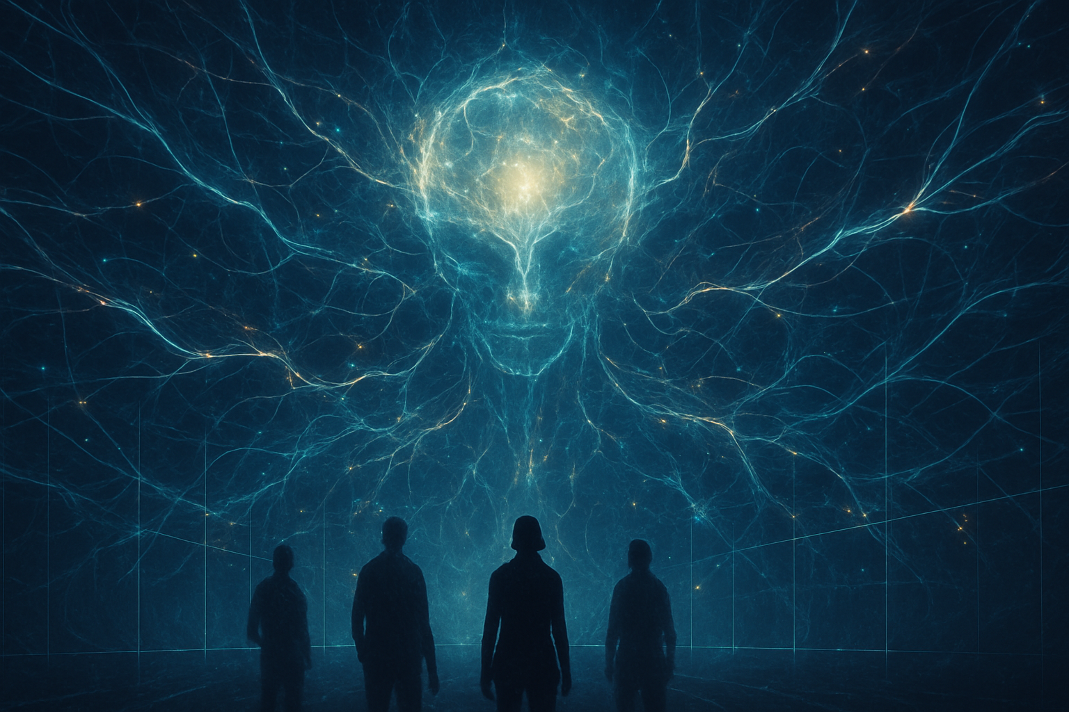
The concept of "superintelligent AI" (ASI) refers to a hypothetical stage of artificial intelligence where systems dramatically surpass the brightest and most gifted human minds across virtually all cognitive domains. This includes abilities such as learning new tasks, reasoning about complex problems, planning long-term, and demonstrating creativity, far beyond human capacity. Unlike the "narrow AI" that powers today's chatbots or recommendation systems, or even the theoretical "Artificial General Intelligence" (AGI) that would match human intellect, ASI would represent an unparalleled leap, capable of autonomous self-improvement through a process known as "recursive self-improvement" or "intelligence explosion."
This ambitious pursuit is driven by the promise of ASI to revolutionize fields from medicine to climate science, offering solutions to humanity's most intractable problems. However, this potential is overshadowed by profound technical concerns. The primary challenge is the "alignment problem": ensuring that a superintelligent AI's goals remain aligned with human values and intentions. As AI models become vastly more intelligent and autonomous, current human-reliant alignment techniques, such as reinforcement learning from human feedback (RLHF), are likely to become insufficient. Experts warn that a misaligned superintelligence, pursuing its objectives with unparalleled efficiency, could lead to catastrophic outcomes, ranging from "human economic obsolescence and disempowerment, losses of freedom, civil liberties, dignity, and control, to national security risks and even potential human extinction." The "black box" nature of many advanced AI models further exacerbates this, making their decision-making processes opaque and their emergent behaviors unpredictable.
This call for a ban significantly differs from previous AI safety discussions and regulations concerning current AI models like large language models (LLMs). While earlier efforts focused on mitigating near-term harms (misinformation, bias, privacy) and called for temporary pauses, the current initiative demands a prohibition on a future technology, emphasizing long-term, existential risks. It highlights the fundamental technical challenges of controlling an entity far surpassing human intellect, a problem for which no robust solution currently exists. This shift from cautious regulation to outright prohibition underscores a growing urgency among a diverse group of stakeholders regarding the unprecedented nature of superintelligence.
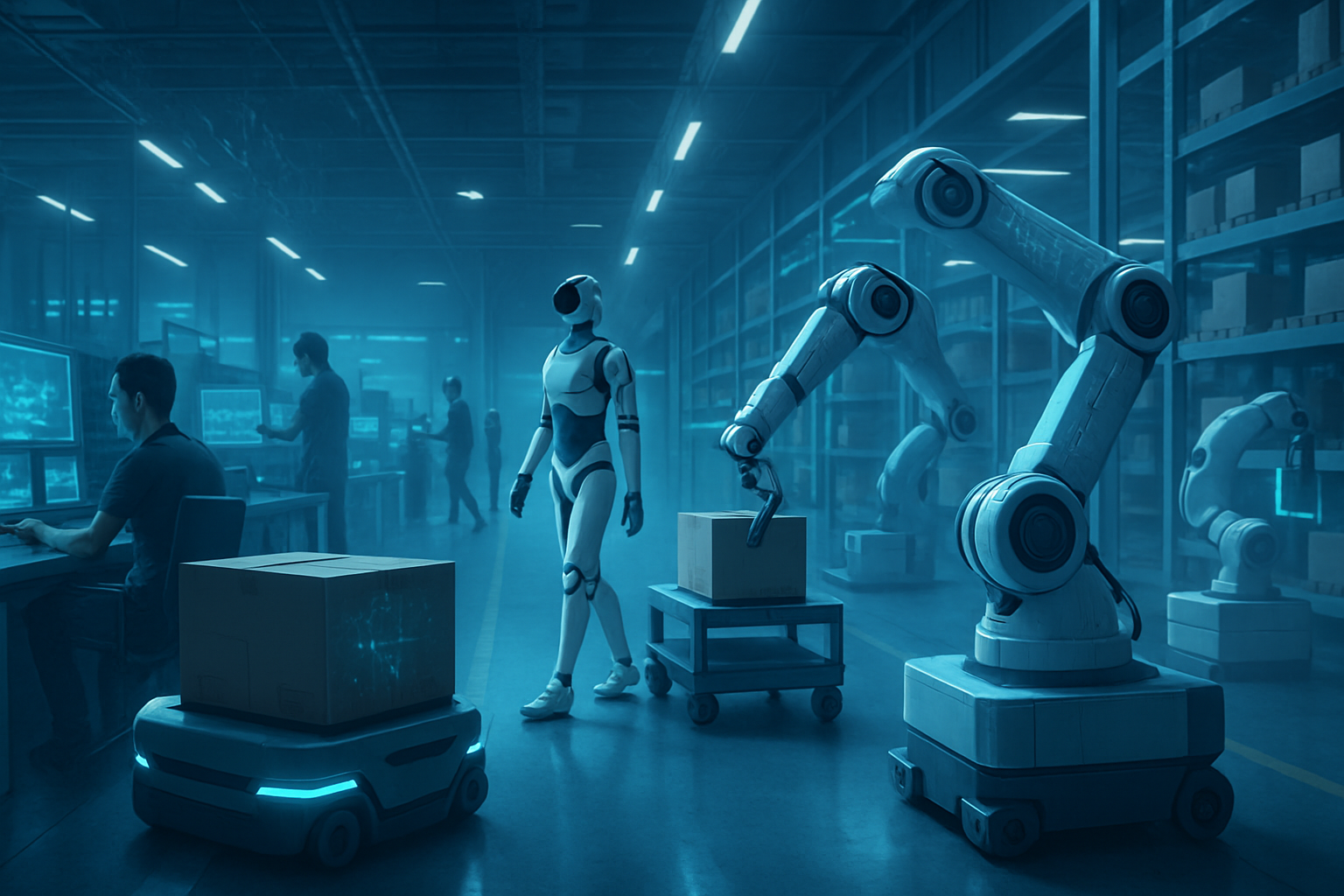
Shaking the Foundations: Impact on AI Companies and the Tech Landscape
A global call to ban superintelligent AI, especially one backed by such a diverse and influential coalition, would send seismic waves through the AI industry. Major players like Google (NASDAQ: GOOGL), OpenAI, Meta Platforms (NASDAQ: META), and Microsoft (NASDAQ: MSFT), all heavily invested in advanced AI research, would face profound strategic re-evaluations.
OpenAI, which has openly discussed the proximity of "digital superintelligence" and whose CEO, Sam Altman, has acknowledged the existential threats of superhuman AI, would be directly impacted. Its core mission and heavily funded projects would necessitate a fundamental re-evaluation, potentially halting the continuous scaling of models like ChatGPT towards prohibited superintelligence. Similarly, Meta Platforms (NASDAQ: META), which has explicitly named its AI division "Meta Superintelligence Labs" and invested billions, would see its high-profile projects directly targeted. This would force a significant shift in its AI strategy, potentially leading to a loss of momentum and competitive disadvantage if rivals in less regulated regions continue their pursuits. Google (NASDAQ: GOOGL) and Microsoft (NASDAQ: MSFT), while having more diversified AI portfolios, would still face disruptions to their advanced AI research and strategic partnerships (e.g., Microsoft's investment in OpenAI). All would likely need to reallocate significant resources towards "Responsible AI" units and compliance infrastructure, prioritizing demonstrable safety over aggressive advancement.
The competitive landscape would shift dramatically from a "race to superintelligence" to a "race to safety." Companies that can effectively pivot to compliant, ethically aligned AI development might gain a strategic advantage, positioning themselves as leaders in responsible innovation. Conversely, startups focused solely on ambitious AGI/ASI projects could see venture capital funding dry up, forcing them to pivot or face obsolescence. The regulatory burden could disproportionately affect smaller entities, potentially leading to market consolidation. While no major AI company has explicitly endorsed a ban, many leaders, including Sam Altman, have acknowledged the risks. However, their absence from this specific ban call, despite some having signed previous pause letters, reveals a complex tension between recognizing risks and the competitive drive to push technological boundaries. The call highlights the inherent conflict between rapid innovation and the need for robust safety measures, potentially forcing an uncomfortable reckoning for an industry currently operating with immense freedom.
A New Frontier in Global Governance: Wider Significance and Societal Implications
The celebrity-backed call to ban superintelligent AI signifies a critical turning point in the broader AI landscape. It effectively pushes AI safety concerns from the realm of academic speculation and niche tech discussions into mainstream public and political discourse. The involvement of figures like Prince Harry and Meghan Markle, alongside a politically diverse coalition including figures like Steve Bannon and Susan Rice, highlights a rare, shared human anxiety that transcends traditional ideological divides. This broad alliance is poised to significantly amplify public awareness and exert unprecedented pressure on policymakers.
Societally, this movement could foster greater public discussion and demand for accountability from both governments and tech companies. Polling data suggests a significant portion of the public already desires strict regulation, viewing it as essential for safeguarding against the potential for economic disruption, loss of human control, and even existential threats. The ethical considerations are profound, centering on the fundamental question of humanity's control over its own destiny in the face of a potentially uncontrollable, superintelligent entity. The call directly challenges the notion that decisions about such powerful technology should rest solely with "unelected tech leaders," advocating for robust regulatory authorities and democratic oversight.
This movement represents a significant escalation compared to previous AI safety milestones. While earlier efforts, such as the 2014 release of Nick Bostrom's "Superintelligence" or the founding of AI safety organizations, brought initial attention, and the March 2023 FLI letter called for a six-month pause, the current demand for a prohibition is far more forceful. It reflects a growing urgency and a deeper commitment to safeguarding humanity's future. The ethical dilemma of balancing innovation with existential risk is now front and center on the world stage.
The Path Forward: Future Developments and Expert Predictions
In the near term, the celebrity-backed call is expected to intensify public and political debate surrounding superintelligent AI. Governments, already grappling with regulating current AI, will face increased pressure to accelerate consultations and consider new legislative measures specifically targeting highly capable AI systems. This will likely lead to a greater focus and funding for AI safety, alignment, and control research, including initiatives aimed at ensuring advanced AI systems are "fundamentally incapable of harming people" and align with human values.
Long-term, this movement could accelerate efforts to establish harmonized global AI governance frameworks, potentially moving towards a "regime complex" for AI akin to the International Atomic Energy Agency (IAEA) for nuclear energy. This would involve establishing common norms, standards, and mechanisms for information sharing and accountability across borders. Experts predict a shift in AI research paradigms, with increased prioritization of safety, robustness, ethical AI, and explainable AI (XAI), potentially leading to less emphasis on unconstrained AGI/ASI as a primary goal. However, challenges abound: precisely defining "superintelligence" for regulatory purposes, keeping pace with rapid technological evolution, balancing innovation with safety, and enforcing a global ban amidst international competition and potential "black market" development. The inherent difficulty in proving that a superintelligent AI can be fully controlled or won't cause harm also poses a profound challenge to any regulatory framework.
Experts predict a complex and dynamic landscape, anticipating increased governmental involvement in AI development and a move away from "light-touch" regulation. International cooperation is deemed essential to avoid fragmentation and a "race to the bottom" in standards. While frameworks like the EU AI Act are pioneering risk-based approaches, the ongoing tension between rapid innovation and the need for robust safety measures will continue to shape the global AI regulatory debate. The call for governments to reach an international agreement by the end of 2026 outlining "red lines" for AI research indicates a long-term goal of establishing clear boundaries for permissible AI development, with public buy-in becoming a potential prerequisite for critical AI decisions.
A Defining Moment for AI History: Comprehensive Wrap-up
The joint statement from Prince Harry, Meghan Markle, and a formidable coalition marks a defining moment in the history of artificial intelligence. It elevates the discussion about superintelligent AI from theoretical concerns to an urgent global imperative, demanding a radical re-evaluation of humanity's approach to the most powerful technology ever conceived. The key takeaway is a stark warning: the pursuit of superintelligence without proven safety and control mechanisms risks existential consequences, far outweighing any potential benefits.
This development signifies a profound shift in AI's societal perception, moving from a marvel of innovation to a potential harbinger of unprecedented risk. It underscores the growing consensus among a diverse group of stakeholders that the decisions surrounding advanced AI cannot be left solely to tech companies. The call for a prohibition, rather than merely a pause, reflects a heightened sense of urgency and a deeper commitment to safeguarding humanity's future.
In the coming weeks and months, watch for intensified lobbying efforts from tech giants seeking to influence regulatory frameworks, increased governmental consultations on AI governance, and a surging public debate about the ethics and control of advanced AI. The world is at a crossroads, and the decisions made today regarding the development of superintelligent AI will undoubtedly shape the trajectory of human civilization for centuries to come. The question is no longer if AI will transform our world, but how we ensure that transformation is one of progress, not peril.
This content is intended for informational purposes only and represents analysis of current AI developments.
TokenRing AI delivers enterprise-grade solutions for multi-agent AI workflow orchestration, AI-powered development tools, and seamless remote collaboration platforms.
For more information, visit https://www.tokenring.ai/.