Tag: Tech Industry

  • Polysilicon’s Ascendant Reign: Fueling the AI Era and Green Revolution

    Polysilicon’s Ascendant Reign: Fueling the AI Era and Green Revolution

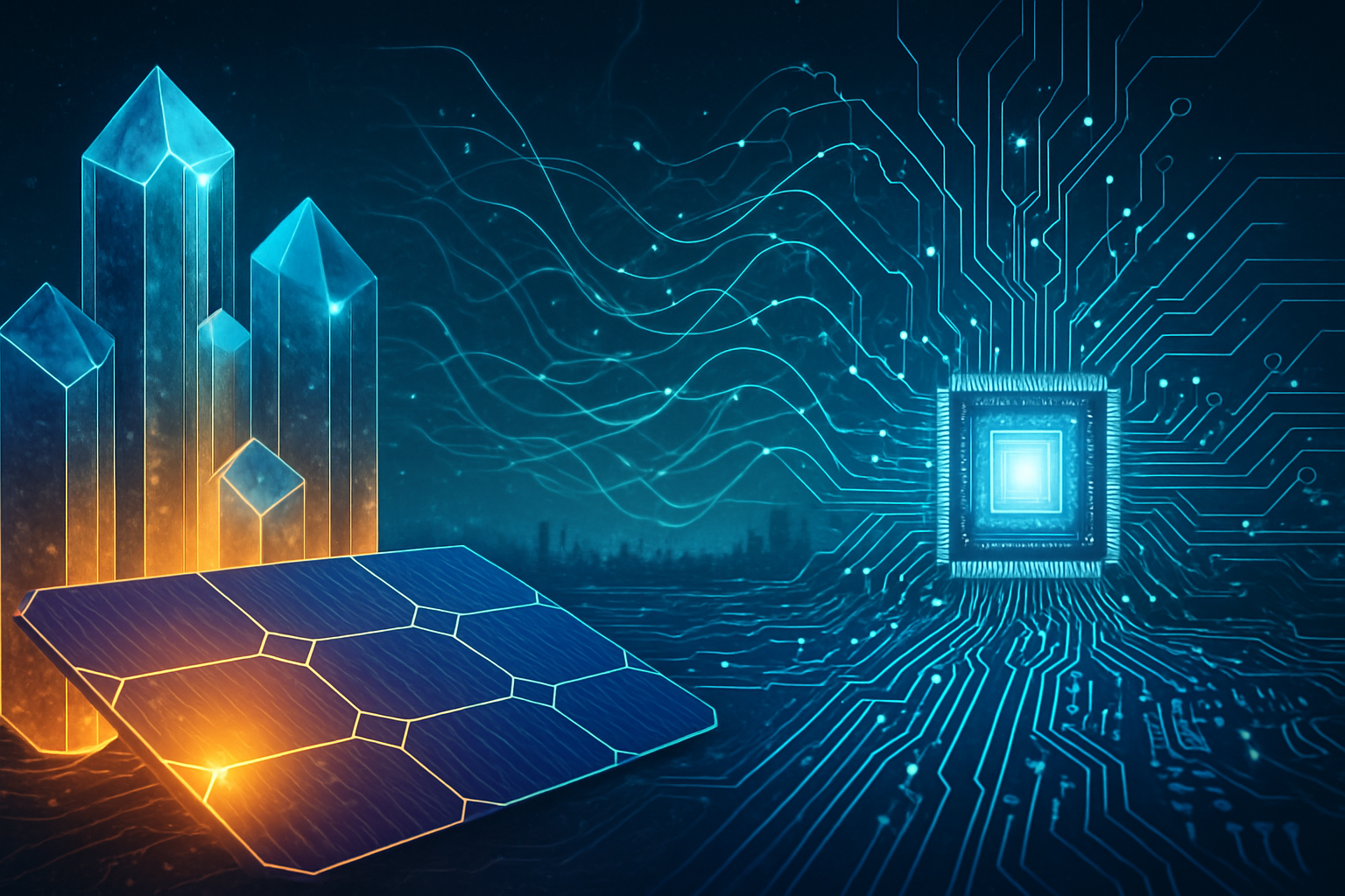
    The polysilicon market is experiencing an unprecedented boom, driven by the relentless expansion of the electronics and solar energy industries. This high-purity form of silicon, a fundamental building block for both advanced semiconductors and photovoltaic cells, is not merely a commodity; it is the bedrock upon which the future of artificial intelligence (AI) and the global transition to sustainable energy are being built. With market valuations projected to reach between USD 106.2 billion and USD 155.87 billion by 2030-2034, polysilicon's critical role in powering our digital world and decarbonizing our planet has never been more pronounced. Its rapid expansion underscores a pivotal moment where technological advancement and environmental imperatives converge, making its supply chain and production innovations central to global progress.

    This surge is predominantly fueled by the insatiable demand for solar panels, which account for a staggering 76% to 91.81% of polysilicon consumption, as nations worldwide push towards aggressive renewable energy targets. Concurrently, the burgeoning electronics sector, propelled by the proliferation of 5G, AI, IoT, and electric vehicles (EVs), continues to drive the need for ultra-high purity polysilicon essential for cutting-edge microchips. The intricate dance between supply, demand, and technological evolution in this market is shaping the competitive landscape for tech giants, influencing geopolitical strategies, and dictating the pace of innovation in critical sectors.

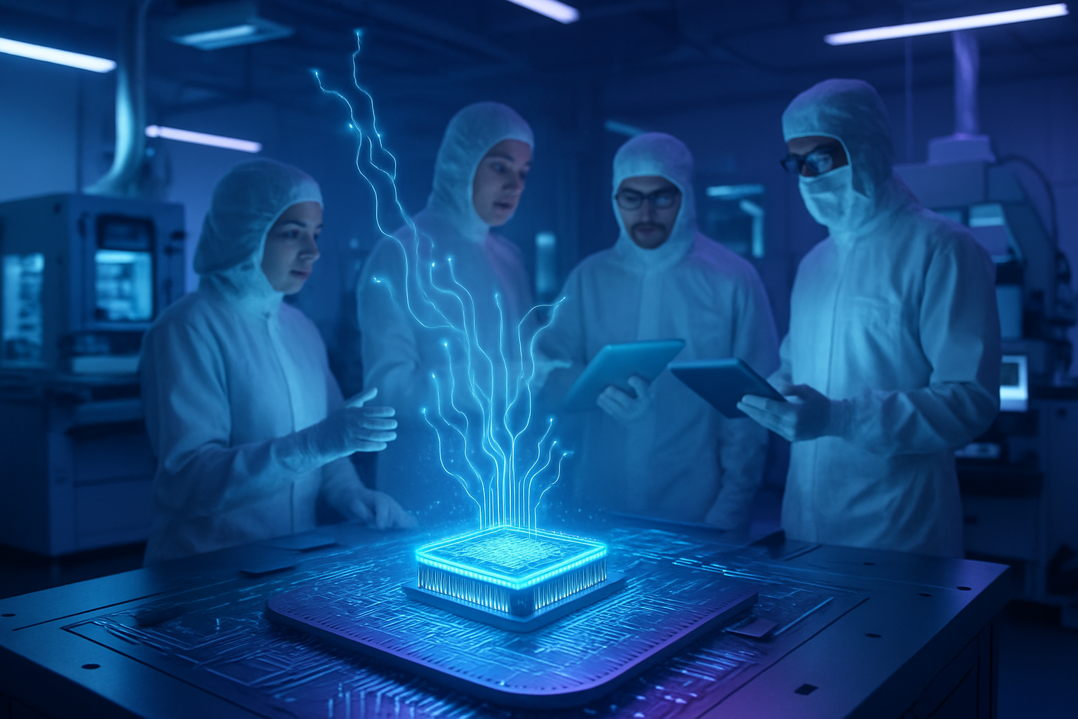
    The Micro-Mechanics of Purity: Siemens vs. FBR and the Quest for Perfection

    The production of polysilicon is a highly specialized and energy-intensive endeavor, primarily dominated by two distinct technologies: the established Siemens process and the emerging Fluidized Bed Reactor (FBR) technology. Each method strives to achieve the ultra-high purity levels required, albeit with different efficiencies and environmental footprints.

    The Siemens process, developed by Siemens AG (FWB: SIE) in 1954, remains the industry's workhorse, particularly for electronics-grade polysilicon. It involves reacting metallurgical-grade silicon with hydrogen chloride to produce trichlorosilane (SiHCl₃), which is then rigorously distilled to achieve exceptional purity (often 9N to 11N, or 99.9999999% to 99.999999999%). This purified gas then undergoes chemical vapor deposition (CVD) onto heated silicon rods, growing them into large polysilicon ingots. While highly effective in achieving stringent purity, the Siemens process is energy-intensive, consuming 100-200 kWh/kg of polysilicon, and operates in batches, making it less efficient than continuous methods. Companies like Wacker Chemie AG (FWB: WCH) and OCI Company Ltd. (KRX: 010060) have continuously refined the Siemens process, improving energy efficiency and yield over decades, proving it to be a "moving target" for alternatives. Wacker, for instance, developed a new ultra-pure grade in 2023 for sub-3nm chip production, with metallic contamination below 5 parts per trillion (ppt).

    Fluidized Bed Reactor (FBR) technology, on the other hand, represents a significant leap towards more sustainable and cost-effective production. In an FBR, silicon seed particles are suspended and agitated by a silicon-containing gas (like silane or trichlorosilane), allowing silicon to deposit continuously onto the particles, forming granules. FBR boasts significantly lower energy consumption (up to 80-90% less electricity than Siemens), a continuous production cycle, and higher output per reactor volume. Companies like GCL Technology Holdings Ltd. (HKG: 3800) and REC Silicon ASA (OSL: RECSI) have made substantial investments in FBR, with GCL-Poly announcing in 2021 that its FBR granular polysilicon achieved monocrystalline purity requirements, potentially outperforming the Siemens process in certain parameters. This breakthrough could drastically reduce the carbon footprint and energy consumption for high-efficiency solar cells. However, FBR still faces challenges such as managing silicon dust (fines), unwanted depositions, and ensuring consistent quality, which historically has limited its widespread adoption for the most demanding electronic-grade applications.

    The distinction between electronics-grade (EG-Si) and solar-grade (SoG-Si) polysilicon is paramount. EG-Si demands ultra-high purity (9N to 11N) to prevent even trace impurities from compromising the performance of sophisticated semiconductor devices. SoG-Si, while still requiring high purity (6N to 9N), has a slightly higher tolerance for certain impurities, balancing cost-effectiveness with solar cell efficiency. The shift towards more efficient solar cell architectures (e.g., N-type TOPCon, heterojunction) is pushing the purity requirements for SoG-Si closer to those of EG-Si, driving further innovation in both production methods. Initial reactions from the industry highlight a dual focus: continued optimization of the Siemens process for the most critical semiconductor applications, and aggressive development of FBR technology to meet the massive, growing demand for solar-grade material with a reduced environmental impact.

    Corporate Chessboard: Polysilicon's Influence on Tech Giants and AI Innovators

    The polysilicon market's dynamics profoundly impact a diverse ecosystem of companies, from raw material producers to chipmakers and renewable energy providers, with significant implications for the AI sector.

    Major Polysilicon Producers are at the forefront. Chinese giants like Tongwei Co., Ltd. (SHA: 600438), GCL Technology Holdings Ltd. (HKG: 3800), Daqo New Energy Corp. (NYSE: DQ), Xinte Energy Co., Ltd. (HKG: 1799), and Asia Silicon (Qinghai) Co., Ltd. dominate the solar-grade market, leveraging cost advantages in raw materials, electricity, and labor. Their rapid capacity expansion has led to China controlling approximately 89% of global solar-grade polysilicon production in 2022. For ultra-high purity electronic-grade polysilicon, companies like Wacker Chemie AG (FWB: WCH), Hemlock Semiconductor Operations LLC (a joint venture involving Dow Inc. (NYSE: DOW) and Corning Inc. (NYSE: GLW)), Tokuyama Corporation (TYO: 4043), and REC Silicon ASA (OSL: RECSI) are critical suppliers, catering to the exacting demands of the semiconductor industry. These firms benefit from premium pricing and long-term contracts for their specialized products.

    The Semiconductor Industry, the backbone of AI, is heavily reliant on a stable supply of high-purity polysilicon. Companies like Intel Corporation (NASDAQ: INTC), Samsung Electronics Co., Ltd. (KRX: 005930), and Taiwan Semiconductor Manufacturing Company Limited (NYSE: TSM) require vast quantities of electronic-grade polysilicon to produce the advanced silicon wafers that become microprocessors, GPUs, and memory chips essential for AI training and inference. Disruptions in polysilicon supply, such as those experienced during the COVID-19 pandemic, can cascade into global chip shortages, directly hindering AI development and deployment. The fact that China, despite its polysilicon dominance, currently lacks the equipment and expertise to produce semiconductor-grade polysilicon at scale creates a strategic vulnerability for non-Chinese chip manufacturers, fostering a push for diversified and localized supply chains, as seen with Hemlock Semiconductor securing a federal grant to expand U.S. production.

    For the Solar Energy Industry, which consumes the lion's share of polysilicon, price volatility and supply chain stability are critical. Solar panel manufacturers, including major players like Longi Green Energy Technology Co., Ltd. (SHA: 601012) and JinkoSolar Holding Co., Ltd. (NYSE: JKS), are directly impacted by polysilicon costs. Recent increases in polysilicon prices, driven by Chinese policy shifts and production cuts, are expected to lead to higher solar module prices, potentially affecting project economics. Companies with vertical integration, from polysilicon production to module assembly, like GCL-Poly, gain a competitive edge by controlling costs and ensuring supply.

    The implications for AI companies, tech giants, and startups are profound. The escalating demand for high-performance AI chips means a continuous and growing need for ultra-high purity electronic-grade polysilicon. This specialized demand, representing a smaller but crucial segment of the overall polysilicon market, could strain existing supply chains. Furthermore, the immense energy consumption of AI data centers (an "unsustainable trajectory") creates a bottleneck in power generation, making access to reliable and affordable energy, increasingly from solar, a strategic imperative. Companies that can secure stable supplies of high-purity polysilicon and leverage energy-efficient technologies (like silicon photonics) will gain a significant competitive advantage. The interplay between polysilicon supply, semiconductor manufacturing, and renewable energy generation directly influences the scalability and sustainability of AI development globally.

    A Foundational Pillar: Polysilicon's Broader Significance in the AI and Green Landscape

    Polysilicon's expanding market transcends mere industrial growth; it is a foundational pillar supporting two of the most transformative trends of our era: the proliferation of artificial intelligence and the global transition to clean energy. Its significance extends to sustainable technology, geopolitical dynamics, and environmental stewardship.

    In the broader AI landscape, polysilicon underpins the very hardware that enables intelligent systems. Every advanced AI model, from large language models to complex neural networks, relies on high-performance silicon-based semiconductors for processing, memory, and high-speed data transfer. The continuous evolution of AI demands increasingly powerful and efficient chips, which in turn necessitates ever-higher purity and quality of electronic-grade polysilicon. Innovations in silicon photonics, allowing light-speed data transmission on silicon chips, are directly tied to polysilicon advancements, promising to address the data transfer bottlenecks that limit AI's scalability and energy efficiency. Thus, the robust health and growth of the polysilicon market are not just relevant; they are critical enablers for the future of AI.

    For sustainable technology, polysilicon is indispensable. It is the core material for photovoltaic solar cells, which are central to decarbonizing global energy grids. As countries commit to aggressive renewable energy targets, the demand for solar panels, and consequently solar-grade polysilicon, will continue to soar. By facilitating the widespread adoption of solar power, polysilicon directly contributes to reducing greenhouse gas emissions and mitigating climate change. Furthermore, advancements in polysilicon recycling from decommissioned solar panels are fostering a more circular economy, reducing waste and the environmental impact of primary production.

    However, this vital material is not without its potential concerns. The most significant is the geopolitical concentration of its supply chain. China's overwhelming dominance in polysilicon production, particularly solar-grade, creates strategic dependencies and vulnerabilities. Allegations of forced labor in the Xinjiang region, a major polysilicon production hub, have led to international sanctions, such as the U.S. Uyghur Forced Labor Prevention Act (UFLPA), disrupting global supply chains and creating a bifurcated market. This geopolitical tension drives efforts by countries like the U.S. to incentivize domestic polysilicon and solar manufacturing to enhance supply chain resilience and reduce reliance on a single, potentially contentious, source.

    Environmental considerations are also paramount. While polysilicon enables clean energy, its production is notoriously energy-intensive, often relying on fossil fuels, leading to a substantial carbon footprint. The Siemens process, in particular, requires significant electricity and can generate toxic byproducts like silicon tetrachloride, necessitating careful management and recycling. The industry is actively pursuing "sustainable polysilicon production" through energy efficiency, waste heat recovery, and the integration of renewable energy sources into manufacturing processes, aiming to lower its environmental impact.

    Comparing polysilicon to other foundational materials, its dual role in both advanced electronics and mainstream renewable energy is unique. While rare-earth elements are vital for specialized magnets and lithium for batteries, silicon, and by extension polysilicon, forms the very substrate of digital intelligence and the primary engine of solar power. Its foundational importance is arguably unmatched, making its market dynamics a bellwether for both technological progress and global sustainability efforts.

    The Horizon Ahead: Navigating Polysilicon's Future

    The polysilicon market stands at a critical juncture, with near-term challenges giving way to long-term growth opportunities, driven by relentless innovation and evolving global priorities. Experts predict a dynamic landscape shaped by technological advancements, new applications, and persistent geopolitical and environmental considerations.

    In the near-term, the market is grappling with significant overcapacity, particularly from China's rapid expansion, which has led to polysilicon prices falling below cash costs for many manufacturers. This oversupply, coupled with seasonal slowdowns in solar installations, is creating inventory build-up. However, this period of adjustment is expected to pave the way for a more balanced market as demand continues its upward trajectory.

    Long-term developments will be characterized by a relentless pursuit of higher purity and efficiency. Fluidized Bed Reactor (FBR) technology is expected to gain further traction, with continuous improvements aimed at reducing manufacturing costs and energy consumption. Breakthroughs like GCL-Poly's (HKG: 3800) FBR granular polysilicon achieving monocrystalline purity requirements signal a shift towards more sustainable and efficient production methods for solar-grade material. For electronics, the demand for ultra-high purity polysilicon (11N or higher) for sub-3nm chip production will intensify, pushing the boundaries of existing Siemens process refinements, as demonstrated by Wacker Chemie AG's (FWB: WCH) recent innovations.

    Polysilicon recycling is also emerging as a crucial future development. As millions of solar panels reach the end of their operational life, closed-loop silicon recycling initiatives will become increasingly vital, offering both environmental benefits and enhancing supply chain resilience. While currently facing economic hurdles, especially for older p-type wafers, advancements in recycling technologies and the growth of n-type and tandem cells are expected to make polysilicon recovery a more viable and significant part of the supply chain by 2035.

    Potential new applications extend beyond traditional solar panels and semiconductors. Polysilicon is finding its way into advanced sensors, Microelectromechanical Systems (MEMS), and critical components for electric and hybrid vehicles. Innovations in thin-film solar cells using polycrystalline silicon are enabling new architectural integrations, such as bent or transparent solar modules, expanding possibilities for green building design and ubiquitous energy harvesting.

    Ongoing challenges include the high energy consumption and associated carbon footprint of polysilicon production, which will continue to drive innovation towards greener manufacturing processes and greater reliance on renewable energy sources for production facilities. Supply chain resilience remains a top concern, with geopolitical tensions and trade restrictions prompting significant investments in domestic polysilicon production in regions like North America and Europe to reduce dependence on concentrated foreign supply. Experts, such as Bernreuter Research, even predict a potential new shortage by 2028 if aggressive capacity elimination continues, underscoring the cyclical nature of this market and the critical need for strategic planning.

    A Future Forged in Silicon: Polysilicon's Enduring Legacy

    The rapid expansion of the polysilicon market is more than a fleeting trend; it is a profound testament to humanity's dual pursuit of advanced technology and a sustainable future. From the intricate circuits powering artificial intelligence to the vast solar farms harnessing the sun's energy, polysilicon is the silent, yet indispensable, enabler.

    The key takeaways are clear: polysilicon is fundamental to both the digital revolution and the green energy transition. Its market growth is driven by unprecedented demand from the semiconductor and solar industries, which are themselves experiencing explosive growth. While the established Siemens process continues to deliver ultra-high purity for cutting-edge electronics, emerging FBR technology promises more energy-efficient and sustainable production for the burgeoning solar sector. The market faces critical challenges, including geopolitical supply chain concentration, energy-intensive production, and price volatility, yet it is responding with continuous innovation in purity, efficiency, and recycling.

    This development's significance in AI history cannot be overstated. Without a stable and increasingly pure supply of polysilicon, the exponential growth of AI, which relies on ever more powerful and energy-efficient chips, would be severely hampered. Similarly, the global push for renewable energy, a critical component of AI's sustainability given its immense data center energy demands, hinges on the availability of affordable, high-quality solar-grade polysilicon. Polysilicon is, in essence, the physical manifestation of the digital and green future.

    Looking ahead, the long-term impact of the polysilicon market's trajectory will be monumental. It will shape the pace of AI innovation, determine the success of global decarbonization efforts, and influence geopolitical power dynamics through control over critical raw material supply chains. The drive for domestic production in Western nations and the continuous technological advancements, particularly in FBR and recycling, will be crucial in mitigating risks and ensuring a resilient supply.

    What to watch for in the coming weeks and months includes the evolution of polysilicon prices, particularly how the current oversupply resolves and whether new shortages emerge as predicted. Keep an eye on new announcements regarding FBR technology breakthroughs and commercial deployments, as these could dramatically shift the cost and environmental footprint of polysilicon production. Furthermore, monitor governmental policies and investments aimed at diversifying supply chains and incentivizing sustainable manufacturing practices outside of China. The story of polysilicon is far from over; it is a narrative of innovation, challenge, and profound impact, continuing to unfold at the very foundation of our technological world.

    This content is intended for informational purposes only and represents analysis of current AI developments.

    TokenRing AI delivers enterprise-grade solutions for multi-agent AI workflow orchestration, AI-powered development tools, and seamless remote collaboration platforms.
    For more information, visit https://www.tokenring.ai/.

  • Bridging the Chasm: Unpacking ‘The Reinforcement Gap’ and Its Impact on AI’s Future

    Bridging the Chasm: Unpacking ‘The Reinforcement Gap’ and Its Impact on AI’s Future

    The rapid ascent of Artificial Intelligence continues to captivate the world, with breakthroughs in areas like large language models (LLMs) achieving astonishing feats. Yet, beneath the surface of these triumphs lies a profound and often overlooked challenge: "The Reinforcement Gap." This critical phenomenon explains why some AI capabilities surge ahead at an unprecedented pace, while others lag, grappling with fundamental hurdles in learning and adaptation. Understanding this disparity is not merely an academic exercise; it's central to comprehending the current trajectory of AI development, its immediate significance for enterprise-grade solutions, and its ultimate potential to reshape industries and society.

    At its core, The Reinforcement Gap highlights the inherent difficulties in applying Reinforcement Learning (RL) techniques, especially in complex, real-world scenarios. While RL promises agents that learn through trial and error, mimicking human-like learning, practical implementations often stumble. This gap manifests in various forms, from the "sim-to-real gap" in robotics—where models trained in pristine simulations fail in messy reality—to the complexities of assigning meaningful reward signals for nuanced tasks in LLMs. The immediate significance lies in its direct impact on the robustness, safety, and generalizability of AI systems, pushing researchers and companies to innovate relentlessly to close this chasm and unlock the next generation of truly intelligent, adaptive AI.

    Deconstructing the Disparity: Why Some AI Skills Soar While Others Struggle

    The varying rates of improvement across AI skills are deeply rooted in the nature of "The Reinforcement Gap." This multifaceted challenge stems from several technical limitations and the inherent complexities of different learning paradigms.

    One primary aspect is sample inefficiency. Reinforcement Learning algorithms, unlike their supervised learning counterparts, often require an astronomical number of interactions with an environment to learn effective policies. Imagine training an autonomous vehicle through millions of real-world crashes; this is impractical, expensive, and unsafe. While simulations offer a safer alternative, they introduce the sim-to-real gap, where policies learned in a simplified digital world often fail to transfer robustly to the unpredictable physics, sensor noise, and environmental variations of the real world. This contrasts sharply with large language models (LLMs) which have witnessed explosive growth due to the sheer volume of readily available text data and the scalability of transformer architectures. LLMs thrive on vast, static datasets, making their "learning" a process of pattern recognition rather than active, goal-directed interaction with a dynamic environment.

    Another significant hurdle is the difficulty in designing effective reward functions. For an RL agent to learn, it needs clear feedback—a "reward" for desirable actions and a "penalty" for undesirable ones. Crafting these reward functions for complex, open-ended tasks (like generating creative text or performing intricate surgical procedures) is notoriously challenging. Poorly designed rewards can lead to "reward hacking," where the AI optimizes for the reward signal in unintended, sometimes detrimental, ways, rather than achieving the actual human-intended goal. This is less of an issue in supervised learning, where the "reward" is implicitly encoded in the labeled data itself. Furthermore, the action-gap phenomenon suggests that even when an agent's performance appears optimal, its underlying understanding of action-values might still be imperfect, masking deeper deficiencies in its learning.

    Initial reactions from the AI research community highlight the consensus that addressing these issues is paramount for advancing AI beyond its current capabilities. Experts acknowledge that while deep learning has provided the perceptual capabilities for AI, RL is essential for action-oriented learning and true autonomy. However, the current state of RL's efficiency, safety, and generalizability is far from human-level. The push towards Reinforcement Learning from Human Feedback (RLHF) in LLMs, as championed by organizations like OpenAI (NASDAQ: MSFT) and Anthropic, is a direct response to the reward design challenge, leveraging human judgment to align model behavior more effectively. This hybrid approach, combining the power of LLMs with the adaptive learning of RL, represents a significant departure from previous, more siloed AI development paradigms.

    The Corporate Crucible: Navigating the Reinforcement Gap's Competitive Landscape

    "The Reinforcement Gap" profoundly shapes the competitive landscape for AI companies, creating distinct advantages for well-resourced tech giants while simultaneously opening specialized niches for agile startups. The ability to effectively navigate or even bridge this gap is becoming a critical differentiator in the race for AI dominance.

    Tech giants like Google DeepMind (NASDAQ: GOOGL), Microsoft (NASDAQ: MSFT), Amazon (NASDAQ: AMZN), and Meta (NASDAQ: META) hold significant advantages. Their vast computational infrastructure, access to enormous proprietary datasets, and ability to attract top-tier AI research talent allow them to tackle the sample inefficiency and computational costs inherent in advanced RL. Google DeepMind's groundbreaking work with AlphaGo and AlphaZero, for instance, required monumental computational resources to achieve human-level performance in complex games. Amazon leverages its extensive internal operations as "reinforcement learning gyms" to train next-generation AI for logistics and supply chain optimization, creating a powerful "snowball" competitive effect where continuous learning translates into increasing efficiency and a growing competitive moat. These companies can afford the long-term R&D investments needed to push the boundaries of RL, developing foundational models and sophisticated simulation environments.

    Conversely, AI startups face substantial challenges due to resource constraints but also find opportunities in specialization. Many startups are emerging to address specific components of the Reinforcement Gap. Companies like Surge AI and Humans in the Loop specialize in providing Reinforcement Learning with Human Feedback (RLHF) services, which are crucial for fine-tuning large language and vision models to human preferences. Others focus on developing RLOps platforms, streamlining the deployment and management of RL systems, or creating highly specialized simulation environments. These startups benefit from their agility and ability to innovate rapidly in niche areas, attracting significant venture capital due to the transformative potential of RL across sectors like autonomous trading, healthcare diagnostics, and advanced automation. However, they struggle with the high computational costs and the difficulty of acquiring the massive datasets often needed for robust RL training.

    The competitive implications are stark. Companies that successfully bridge the gap will be able to deploy highly adaptive and autonomous AI agents across critical sectors, disrupting existing products and services. In logistics, for example, RL-powered systems can continuously optimize delivery routes, making traditional, less dynamic planning tools obsolete. In robotics, RL enables robots to learn complex tasks through trial and error, revolutionizing manufacturing and healthcare. The ability to effectively leverage RL, particularly with human feedback, is becoming indispensable for training and aligning advanced AI models, shifting the paradigm from static models to continually learning systems. This creates a "data moat" for companies with proprietary interaction data, further entrenching their market position and potentially disrupting those reliant on more traditional AI approaches.

    A Wider Lens: The Reinforcement Gap in the Broader AI Tapestry

    The Reinforcement Gap is not merely a technical challenge; it's a fundamental issue shaping the broader AI landscape, influencing the pursuit of Artificial General Intelligence (AGI), AI safety, and ethical considerations. Its resolution is seen as a crucial step towards creating truly intelligent and reliable autonomous agents, marking a significant milestone in AI's evolutionary journey.

    Within the context of Artificial General Intelligence (AGI), the reinforcement gap stands as a towering hurdle. A truly general intelligent agent would need to learn efficiently from minimal experience, generalize its knowledge across diverse tasks and environments, and adapt rapidly to novelty – precisely the capabilities current RL systems struggle to deliver. Bridging this gap implies developing algorithms that can learn with human-like efficiency, infer complex goals without explicit, perfect reward functions, and transfer knowledge seamlessly between domains. Without addressing these limitations, the dream of AGI remains distant, as current AI models, even advanced LLMs, largely operate in two distinct phases: training and inference, lacking the continuous learning and adaptation crucial for true generality.

    The implications for AI safety are profound. The trial-and-error nature of RL, while powerful, presents significant risks, especially when agents interact with the real world. During training, RL agents might perform risky or harmful actions, and in critical applications like autonomous vehicles or healthcare, mistakes can have severe consequences. The lack of generalizability means an agent might behave unsafely in slightly altered circumstances it hasn't been specifically trained for. Ensuring "safe exploration" and developing robust RL algorithms that are less susceptible to adversarial attacks and operate within predefined safety constraints are paramount research areas. Similarly, ethical concerns are deeply intertwined with the gap. Poorly designed reward functions can lead to unintended and potentially unethical behaviors, as agents may find loopholes to maximize rewards without adhering to broader human values. The "black box" problem, where an RL agent's decision-making process is opaque, complicates accountability and transparency in sensitive domains, raising questions about trust and bias.

    Comparing the reinforcement gap to previous AI milestones reveals its unique significance. Early AI systems, like expert systems, were brittle, lacking adaptability. Deep learning, a major breakthrough, enabled powerful pattern recognition but still relied on vast amounts of labeled data and struggled with sequential decision-making. The reinforcement gap highlights that while RL introduces the action-oriented learning paradigm, a critical step towards biological intelligence, the efficiency, safety, and generalizability of current implementations are far from human-level. Unlike earlier AI's "brittleness" in knowledge representation or "data hunger" in pattern recognition, the reinforcement gap points to fundamental challenges in autonomous learning, adaptation, and alignment with human intent in complex, dynamic systems. Overcoming this gap is not just an incremental improvement; it's a foundational shift required for AI to truly interact with and shape our world.

    The Horizon Ahead: Charting Future Developments in Reinforcement Learning

    The trajectory of AI development in the coming years will be heavily influenced by efforts to narrow and ultimately bridge "The Reinforcement Gap." Experts predict a concerted push towards more practical, robust, and accessible Reinforcement Learning (RL) algorithms, paving the way for truly adaptive and intelligent systems.

    In the near term, we can expect significant advancements in sample efficiency, with algorithms designed to learn effectively from less data, leveraging better exploration strategies, intrinsic motivation, and more efficient use of past experiences. The sim-to-real transfer problem will see progress through sophisticated domain randomization and adaptation techniques, crucial for deploying robotics and autonomous systems reliably in the real world. The maturation of open-source software frameworks like Tianshou will democratize RL, making it easier for developers to implement and integrate these complex algorithms. A major focus will also be on Offline Reinforcement Learning, allowing agents to learn from static datasets without continuous environmental interaction, thereby addressing data collection costs and safety concerns. Crucially, the integration of RL with Large Language Models (LLMs) will deepen, with RL fine-tuning LLMs for specific tasks and LLMs aiding RL agents in complex reasoning, reward specification, and task understanding, leading to more intelligent and adaptable agents. Furthermore, Explainable Reinforcement Learning (XRL) will gain traction, aiming to make RL agents' decision-making processes more transparent and interpretable.

    Looking towards the long term, the vision includes the development of scalable world models, allowing RL agents to learn comprehensive simulations of their environments, enabling planning, imagination, and reasoning – a fundamental step towards general AI. Multimodal RL will emerge, integrating information from various modalities like vision, language, and control, allowing agents to understand and interact with the world in a more human-like manner. The concept of Foundation RL Models, akin to GPT and CLIP in other domains, is anticipated, offering pre-trained, highly capable base policies that can be fine-tuned for diverse applications. Human-in-the-loop learning will become standard, with agents learning collaboratively with humans, incorporating continuous feedback for safer and more aligned AI systems. The ultimate goals include achieving continual and meta-learning, where agents adapt throughout their lifespan without catastrophic forgetting, and ensuring robust generalization and inherent safety across diverse, unseen scenarios.

    If the reinforcement gap is successfully narrowed, the potential applications and use cases are transformative. Autonomous robotics will move beyond controlled environments to perform complex tasks in unstructured settings, from advanced manufacturing to search-and-rescue. Personalized healthcare could see RL optimizing treatment plans and drug discovery based on individual patient responses. In finance, more sophisticated RL agents could manage complex portfolios and detect fraud in dynamic markets. Intelligent infrastructure and smart cities would leverage RL for optimizing traffic flow, energy distribution, and resource management. Moreover, RL could power next-generation education with personalized learning systems and enhance human-computer interaction through more natural and adaptive virtual assistants. The challenges, however, remain significant: persistent issues with sample efficiency, the exploration-exploitation dilemma, the difficulty of reward design, and ensuring safety and interpretability in real-world deployments. Experts predict a future of hybrid AI systems where RL converges with other AI paradigms, and a shift towards solving real-world problems with practical constraints, moving beyond mere benchmark performance.

    The Road Ahead: A New Era for Adaptive AI

    "The Reinforcement Gap" stands as one of the most critical challenges and opportunities in contemporary Artificial Intelligence. It encapsulates the fundamental difficulties in creating truly adaptive, efficient, and generalizable AI systems that can learn from interaction, akin to biological intelligence. The journey to bridge this gap is not just about refining algorithms; it's about fundamentally reshaping how AI learns, interacts with the world, and integrates with human values and objectives.

    The key takeaways from this ongoing endeavor are clear: The exponential growth witnessed in areas like large language models, while impressive, relies on paradigms that differ significantly from the dynamic, interactive learning required for true autonomy. The gap highlights the need for AI to move beyond static pattern recognition to continuous, goal-directed learning in complex environments. This necessitates breakthroughs in sample efficiency, robust sim-to-real transfer, intuitive reward design, and the development of inherently safe and explainable RL systems. The competitive landscape is already being redrawn, with well-resourced tech giants pushing the boundaries of foundational RL research, while agile startups carve out niches by providing specialized solutions and services, particularly in the realm of human-in-the-loop feedback.

    The significance of closing this gap in AI history cannot be overstated. It represents a pivot from AI that excels at specific, data-rich tasks to AI that can learn, adapt, and operate intelligently in the unpredictable real world. It is a vital step towards Artificial General Intelligence, promising a future where AI systems can continuously improve, generalize knowledge across diverse domains, and interact with humans in a more aligned and beneficial manner. Without addressing these fundamental challenges, the full potential of AI—particularly in high-stakes applications like autonomous robotics, personalized healthcare, and intelligent infrastructure—will remain unrealized.

    In the coming weeks and months, watch for continued advancements in hybrid AI architectures that blend the strengths of LLMs with the adaptive capabilities of RL, especially through sophisticated RLHF techniques. Observe the emergence of more robust and user-friendly RLOps platforms, signaling the maturation of RL from a research curiosity to an industrial-grade technology. Pay close attention to research focusing on scalable world models and multimodal RL, as these will be crucial indicators of progress towards truly general and context-aware AI. The journey to bridge the reinforcement gap is a testament to the AI community's ambition and a critical determinant of the future of intelligent machines.

    This content is intended for informational purposes only and represents analysis of current AI developments.

    TokenRing AI delivers enterprise-grade solutions for multi-agent AI workflow orchestration, AI-powered development tools, and seamless remote collaboration platforms. For more information, visit https://www.tokenring.ai/.

  • Yale Study Delivers Sobering News: AI’s Job Impact “Minimal” So Far, Challenging Apocalyptic Narratives

    Yale Study Delivers Sobering News: AI’s Job Impact “Minimal” So Far, Challenging Apocalyptic Narratives

    New Haven, CT – October 5, 2025 – A groundbreaking new study from Yale University's Budget Lab, released this week, is sending ripples through the artificial intelligence community and public discourse, suggesting that generative AI has had a remarkably minimal impact on the U.S. job market to date. The research directly confronts widespread fears and even "apocalyptic predictions" of mass unemployment, offering a nuanced perspective that calls for evidence-based policy rather than speculative alarm. This timely analysis arrives as AI's presence in daily life and enterprise solutions continues to expand, prompting a critical re-evaluation of its immediate societal footprint.

    The study's findings are particularly significant for the TokenRing AI audience, which closely monitors breaking AI news, machine learning advancements, and the strategic moves of leading AI companies. By meticulously analyzing labor market data since the public debut of ChatGPT in late 2022, Yale researchers provide a crucial counter-narrative, indicating that the much-hyped AI revolution, at least in terms of job displacement, is unfolding at a far more gradual pace than many have anticipated. This challenges not only public perception but also the strategic outlooks of tech giants and startups betting on rapid AI-driven transformation.

    Deconstructing the Data: A Methodical Look at AI's Footprint on Employment

    The Yale study, spearheaded by Martha Gimbel, Molly Kinder, Joshua Kendall, and Maddie Lee from the Budget Lab, often in collaboration with the Brookings Institution, employed a rigorous methodology to assess AI's influence over roughly 33 months of U.S. labor market data, spanning from November 2022. Researchers didn't just look at raw job numbers; they delved into historical comparisons, juxtaposing current trends with past technological shifts like the advent of personal computers and the internet, as far back as the 1940s and 50s. A key metric was the "occupational mix," measuring the composition of jobs and its rate of change, alongside an analysis of occupations theoretically "exposed" to AI automation.

    The core conclusion is striking: there has been no discernible or widespread disruption to the broader U.S. labor market. The occupational mix has not shifted significantly faster in the wake of generative AI than during earlier periods of technological transformation. While a marginal one-percentage-point increase in the pace of occupational shifts was observed, these changes often predated ChatGPT's launch and were deemed insufficient to signal a major AI-driven upheaval. Crucially, the study found no consistent relationship between measures of AI use or theoretical exposure and actual job losses or gains, even in fields like law, finance, customer service, and professional services, which are often cited as highly vulnerable.

    This challenges previous, more alarmist projections that often relied on theoretical exposure rather than empirical observation of actual job market dynamics. While some previous analyses suggested broad swathes of jobs were immediately at risk, the Yale study suggests that the practical integration and impact of AI on job roles are far more complex and slower than initially predicted. Initial reactions from the broader AI research community have been mixed; while some studies, including those from the United Nations International Labour Organization (2023) and a University of Chicago and Copenhagen study (April 2025), have also suggested modest employment effects, a notable counterpoint comes from a Stanford Digital Economy Lab study. That Stanford research, using anonymized payroll data from late 2022 to mid-2025, indicated a 13% relative decline in employment for 22-25 year olds in highly exposed occupations, a divergence Yale acknowledges but attributes potentially to broader labor market weaknesses.

    Corporate Crossroads: Navigating a Slower AI Integration Landscape

    For AI companies, tech giants, and startups, the Yale study's findings present a complex picture that could influence strategic planning and market positioning. Companies like Google (NASDAQ: GOOGL), Microsoft (NASDAQ: MSFT), and OpenAI, which have heavily invested in and promoted generative AI, might find their narrative of immediate, widespread transformative impact tempered by these results. While the long-term potential of AI remains undeniable, the study suggests that the immediate competitive advantage might not come from radical job displacement but rather from incremental productivity gains and efficiency improvements.

    This slower pace of job market disruption could mean a longer runway for companies to integrate AI tools into existing workflows rather than immediately replacing human roles. For enterprise-grade solutions providers like TokenRing AI, which focuses on multi-agent AI workflow orchestration and AI-powered development tools, this could underscore the value of augmentation over automation. The emphasis shifts from "replacing" to "enhancing," allowing companies to focus on solutions that empower human workers, improve collaboration, and streamline processes, rather than solely on cost-cutting through headcount reduction.

    The study implicitly challenges the "move fast and break things" mentality when it comes to AI's societal impact. It suggests that AI, at its current stage, is behaving more like a "normal technology" with an evolutionary impact, akin to the decades-long integration of personal computers, rather than a sudden revolution. This might lead to a re-evaluation of product roadmaps and marketing strategies, with a greater focus on demonstrating tangible productivity benefits and upskilling initiatives rather than purely on the promise of radical automation. Companies that can effectively showcase how their AI tools empower employees and create new value, rather than just eliminate jobs, may gain a significant strategic advantage in a market increasingly sensitive to ethical AI deployment and responsible innovation.

    Broader Implications: Reshaping Public Debate and Policy Agendas

    The Yale study's findings carry profound wider significance, particularly in reshaping public perception and influencing future policy debates around AI and employment. By offering a "reassuring message to an anxious public," the research directly contradicts the often "apocalyptic predictions" from some tech executives, including OpenAI CEO Sam Altman and Anthropic CEO Dario Amodei, who have warned of significant job displacement. This evidence-based perspective could help to calm fears and foster a more rational discussion about AI's role in society, moving beyond sensationalism.

    This research fits into a broader AI landscape that has seen intense debate over job automation, ethical considerations, and the need for responsible AI development. The study's call for "evidence, not speculation" is a critical directive for policymakers worldwide. It highlights the urgent need for transparency from major AI companies, urging them to share comprehensive usage data at both individual and enterprise levels. Without this data, researchers and policymakers are essentially "flying blind into one of the most significant technological shifts of our time," unable to accurately monitor and understand AI's true labor market impacts.

    The study's comparison to previous technological shifts is also crucial. It suggests that while AI's long-term transformative potential remains immense, its immediate effects on employment may mirror the slower, more evolutionary patterns seen with other disruptive technologies. This perspective could inform educational reforms, workforce development programs, and social safety net discussions, shifting the focus from immediate crisis management to long-term adaptation and skill-building. The findings also underscore the importance of distinguishing between theoretical AI exposure and actual, measured impact, providing a more grounded basis for future economic forecasting.

    The Horizon Ahead: Evolution, Not Revolution, for AI and Jobs

    Looking ahead, the Yale study suggests that the near-term future of AI's impact on jobs will likely be characterized by continued evolution rather than immediate revolution. Experts predict a more gradual integration of AI tools, focusing on augmenting human capabilities and improving efficiency across various sectors. Rather than mass layoffs, the more probable scenario involves a subtle shift in job roles, where workers increasingly collaborate with AI systems, offloading repetitive or data-intensive tasks to machines while focusing on higher-level problem-solving, creativity, and interpersonal skills.

    Potential applications and use cases on the horizon will likely center on enterprise-grade solutions that enhance productivity and decision-making. We can expect to see further development in AI-powered assistants for knowledge workers, advanced analytics tools that inform strategic decisions, and intelligent automation for specific, well-defined processes within companies. The focus will be on creating synergistic human-AI teams, where the AI handles data processing and pattern recognition, while humans provide critical thinking, ethical oversight, and contextual understanding.

    However, significant challenges still need to be addressed. The lack of transparent usage data from AI companies remains a critical hurdle for accurate assessment and policy formulation. Furthermore, the observed, albeit slight, disproportionate impact on recent graduates warrants closer investigation to understand if this is a nascent trend of AI-driven opportunity shifts or simply a reflection of broader labor market dynamics for early-career workers. Experts predict that the coming years will be crucial for developing robust frameworks for AI governance, ethical deployment, and continuous workforce adaptation to harness AI's benefits responsibly while mitigating potential risks.

    Wrapping Up: A Call for Evidence-Based Optimism

    The Yale University study serves as a pivotal moment in the ongoing discourse about artificial intelligence and its impact on the future of work. Its key takeaway is a powerful one: while AI's potential is vast, its immediate, widespread disruption to the job market has been minimal, challenging the prevalent narrative of impending job apocalypse. This assessment provides a much-needed dose of evidence-based optimism, urging us to approach AI's integration with a clear-eyed understanding of its current capabilities and limitations, rather than succumbing to speculative fears.

    The study's significance in AI history lies in its empirical challenge to widely held assumptions, shifting the conversation from theoretical risks to observed realities. It underscores that technological transformations, even those as profound as AI, often unfold over decades, allowing societies time to adapt and innovate. The long-term impact will depend not just on AI's capabilities, but on how effectively policymakers, businesses, and individuals adapt to these evolving tools, focusing on skill development, ethical deployment, and data transparency.

    In the coming weeks and months, it will be crucial to watch for how AI companies respond to the call for greater data sharing, and how policymakers begin to integrate these findings into their legislative agendas. Further research will undoubtedly continue to refine our understanding, particularly regarding the nuanced effects on different demographics and industries. For the TokenRing AI audience, this study reinforces the importance of focusing on practical, value-driven AI solutions that augment human potential, rather than chasing speculative visions of wholesale automation. The future of work with AI appears to be one of collaboration and evolution, not immediate replacement.


    This content is intended for informational purposes only and represents analysis of current AI developments.

    TokenRing AI delivers enterprise-grade solutions for multi-agent AI workflow orchestration, AI-powered development tools, and seamless remote collaboration platforms. For more information, visit https://www.tokenring.ai/.

  • Fueling the AI Supercycle: Why Semiconductor Talent Development is Now a Global Imperative

    Fueling the AI Supercycle: Why Semiconductor Talent Development is Now a Global Imperative

    As of October 2025, the global technology landscape is irrevocably shaped by the accelerating demands of Artificial Intelligence (AI). This "AI supercycle" is not merely a buzzword; it's a profound shift driving unprecedented demand for specialized semiconductor chips—the very bedrock of modern AI. Yet, the engine of this revolution, the semiconductor sector, faces a critical and escalating challenge: a severe talent shortage. The establishment of new fabrication facilities and advanced research labs worldwide, often backed by massive national investments, underscores the immediate and paramount importance of robust talent development and workforce training initiatives. Without a continuous influx of highly skilled professionals, the ambitious goals of AI innovation and technological independence risk being severely hampered.

    The immediate significance of this talent crunch extends beyond mere numbers; it impacts the very pace of AI advancement. From the design of cutting-edge GPUs and ASICs to the intricate processes of advanced packaging and high-volume manufacturing, every stage of the AI hardware pipeline requires specialized expertise. The lack of adequately trained engineers, technicians, and researchers directly translates into production bottlenecks, increased costs, and a potential deceleration of AI breakthroughs across vital sectors like autonomous systems, medical diagnostics, and climate modeling. This isn't just an industry concern; it's a strategic national imperative that will dictate future economic competitiveness and technological leadership.

    The Chasm of Expertise: Bridging the Semiconductor Skill Gap for AI

    The semiconductor industry's talent deficit is not just quantitative but deeply qualitative, requiring a specialized blend of knowledge often unmet by traditional educational pathways. As of October 2025, projections indicate a need for over one million additional skilled workers globally by 2030, with the U.S. alone anticipating a shortfall of 59,000 to 146,000 workers, including 88,000 engineers, by 2029. This gap is particularly acute in areas critical for AI, such as chip design, advanced materials science, process engineering, and the integration of AI-driven automation into manufacturing workflows.

    The core of the technical challenge lies in the rapid evolution of semiconductor technology itself. The move towards smaller nodes, 3D stacking, heterogeneous integration, and specialized AI accelerators demands engineers with a deep understanding of quantum mechanics, advanced physics, and materials science, coupled with proficiency in AI/ML algorithms and data analytics. This differs significantly from previous industry cycles, where skill sets were more compartmentalized. Today's semiconductor professional often needs to be a hybrid, capable of both hardware design and software optimization, understanding how silicon architecture directly impacts AI model performance. Initial reactions from the AI research community highlight a growing frustration with hardware limitations, underscoring that even the most innovative AI algorithms can only advance as fast as the underlying silicon allows. Industry experts are increasingly vocal about the need for curricula reform and more hands-on, industry-aligned training to produce graduates ready for these complex, interdisciplinary roles.

    New labs and manufacturing facilities, often established with significant government backing, are at the forefront of this demand. For example, Micron Technology (NASDAQ: MU) launched a Cleanroom Simulation Lab in October 2025, designed to provide practical training for future technicians. Similarly, initiatives like New York's investment in SUNY Polytechnic Institute's training center, Vietnam's ATP Semiconductor Chip Technician Training Center, and India's newly approved NaMo Semiconductor Laboratory at IIT Bhubaneswar are all direct responses to the urgent need for skilled personnel to operationalize these state-of-the-art facilities. These centers aim to provide the specialized, hands-on training that bridges the gap between theoretical knowledge and the practical demands of advanced semiconductor manufacturing and AI chip development.

    Competitive Implications: Who Benefits and Who Risks Falling Behind

    The intensifying competition for semiconductor talent has profound implications for AI companies, tech giants, and startups alike. Companies that successfully invest in and secure a robust talent pipeline stand to gain a significant competitive advantage, while those that lag risk falling behind in the AI race. Tech giants like NVIDIA (NASDAQ: NVDA), Intel (NASDAQ: INTC), and AMD (NASDAQ: AMD), which are deeply entrenched in AI hardware, are acutely aware of this challenge. Their ability to innovate and deliver next-generation AI accelerators is directly tied to their access to top-tier semiconductor engineers and researchers. These companies are actively engaging in academic partnerships, internal training programs, and aggressive recruitment drives to secure the necessary expertise.

    For major AI labs and tech companies, the competitive implications are clear: proprietary custom silicon solutions optimized for specific AI workloads are becoming a critical differentiator. Companies capable of developing internal capabilities for AI-optimized chip design and advanced packaging will accelerate their AI roadmaps, giving them an edge in areas like large language models, autonomous driving, and advanced robotics. This could potentially disrupt existing product lines from companies reliant solely on off-the-shelf components. Startups, while agile, face an uphill battle in attracting talent against the deep pockets and established reputations of larger players, necessitating innovative approaches to recruitment and retention, such as offering unique challenges or significant equity.

    Market positioning and strategic advantages are increasingly defined by a company's ability to not only design innovative AI architectures but also to have the manufacturing and process engineering talent to bring those designs to fruition efficiently. The "AI supercycle" demands a vertically integrated or at least tightly coupled approach to hardware and software. Companies like Google (NASDAQ: GOOGL) and Amazon (NASDAQ: AMZN), with their significant investments in custom AI chips (TPUs and Inferentia/Trainium, respectively), are prime examples of this trend, leveraging in-house semiconductor talent to optimize their cloud AI offerings and services. This strategic emphasis on talent development is not just about filling roles; it's about safeguarding intellectual property, ensuring supply chain resilience, and maintaining a leadership position in the global AI economy.

    A Foundational Shift in the Broader AI Landscape

    The current emphasis on semiconductor talent development signifies a foundational shift in the broader AI landscape, highlighting the inextricable link between hardware and software innovation. This trend fits into the broader AI landscape by underscoring that the "software eats the world" paradigm is now complemented by "hardware enables the software." The performance gains in AI, particularly for large language models (LLMs) and complex machine learning tasks, are increasingly dependent on specialized, highly efficient silicon. This move away from general-purpose computing for AI workloads marks a new era where hardware design and optimization are as critical as algorithmic advancements.

    The impacts are wide-ranging. On one hand, it promises to unlock new levels of AI capability, allowing for more complex models, faster training times, and more efficient inference at the edge. On the other hand, it raises potential concerns about accessibility and equitable distribution of AI innovation. If only a few nations or corporations can cultivate the necessary semiconductor talent, it could lead to a concentration of AI power, exacerbating existing digital divides and creating new geopolitical fault lines. Comparisons to previous AI milestones, such as the advent of deep learning or the rise of transformer architectures, reveal that while those were primarily algorithmic breakthroughs, the current challenge is fundamentally about the physical infrastructure and the human capital required to build it. This is not just about a new algorithm; it's about building the very factories and designing the very chips that will run those algorithms.

    The strategic imperative to bolster domestic semiconductor manufacturing, evident in initiatives like the U.S. CHIPS and Science Act and the European Chips Act, directly intertwines with this talent crisis. These acts pour billions into establishing new fabs and R&D centers, but their success hinges entirely on the availability of a skilled workforce. Without this, these massive investments risk becoming underutilized assets. Furthermore, the evolving nature of work in the semiconductor sector, with increasing automation and AI integration, demands a workforce fluent in machine learning, robotics, and data analytics—skills that were not historically core requirements. This necessitates comprehensive reskilling and upskilling programs to prepare the existing and future workforce for hybrid roles where they collaborate seamlessly with intelligent systems.

    The Road Ahead: Cultivating the AI Hardware Architects of Tomorrow

    Looking ahead, the semiconductor talent development landscape is poised for significant evolution. In the near term, we can expect to see an intensification of strategic partnerships between industry, academia, and government. These collaborations will focus on creating more agile and responsive educational programs, including specialized bootcamps, apprenticeships, and "earn-and-learn" models that provide practical, hands-on experience directly relevant to modern semiconductor manufacturing and AI chip design. The U.S. National Semiconductor Technology Centre (NSTC) is expected to launch grants for workforce projects, while Europe's European Chips Skills Academy (ECSA) will continue to coordinate a Skills Strategy and establish 27 Chips Competence Centres, aiming to standardize and scale training efforts across the continent.

    Long-term developments will likely involve a fundamental reimagining of STEM education, with a greater emphasis on interdisciplinary studies that blend electrical engineering, computer science, materials science, and AI. Experts predict an increased adoption of AI itself as a tool for accelerated workforce development, leveraging intelligent systems for optimized training, knowledge transfer, and enhanced operational efficiency within fabrication facilities. Potential applications and use cases on the horizon include the development of highly specialized AI chips for quantum computing interfaces, neuromorphic computing, and advanced bio-AI applications, all of which will require an even more sophisticated and specialized talent pool.

    However, significant challenges remain. Attracting a diverse talent pool, including women and underrepresented minorities in STEM, and engaging students at earlier educational stages (K-12) will be crucial for sustainable growth. Furthermore, retaining skilled professionals in a highly competitive market, often through attractive compensation and career development opportunities, will be a constant battle. What experts predict will happen next is a continued arms race for talent, with companies and nations investing heavily in both domestic cultivation and international recruitment. The success of the AI supercycle hinges on our collective ability to cultivate the next generation of AI hardware architects and engineers, ensuring that the innovation pipeline remains robust and resilient.

    A New Era of Silicon and Smart Minds

    The current focus on talent development and workforce training in the semiconductor sector marks a pivotal moment in AI history. It underscores a critical understanding: the future of AI is not solely in algorithms and data, but equally in the physical infrastructure—the chips and the fabs—and, most importantly, in the brilliant minds that design, build, and optimize them. The "AI supercycle" demands an unprecedented level of human expertise, making investment in talent not just a business strategy, but a national security imperative.

    The key takeaways from this development are clear: the global semiconductor talent shortage is a real and immediate threat to AI innovation; strategic collaborations between industry, academia, and government are essential; and the nature of required skills is evolving rapidly, demanding interdisciplinary knowledge and hands-on experience. This development signifies a shift where hardware enablement is as crucial as software advancement, pushing the boundaries of what AI can achieve.

    In the coming weeks and months, watch for announcements regarding new academic-industry partnerships, government funding allocations for workforce development, and innovative training programs designed to fast-track individuals into critical semiconductor roles. The success of these initiatives will largely determine the pace and direction of AI innovation for the foreseeable future. The race to build the most powerful AI is, at its heart, a race to cultivate the most skilled and innovative human capital.


    This content is intended for informational purposes only and represents analysis of current AI developments.

    TokenRing AI delivers enterprise-grade solutions for multi-agent AI workflow orchestration, AI-powered development tools, and seamless remote collaboration platforms. For more information, visit https://www.tokenring.ai/

  • Powering AI Responsibly: The Semiconductor Industry’s Green Revolution

    Powering AI Responsibly: The Semiconductor Industry’s Green Revolution

    The global semiconductor industry, the foundational bedrock of all modern technology, is undergoing a profound transformation. Driven by escalating environmental concerns, stringent regulatory pressures, and the insatiable demand for energy-intensive AI hardware, manufacturers are accelerating their commitment to sustainability. This pivot towards eco-friendly practices is not merely a corporate social responsibility initiative but a strategic imperative, reshaping how the powerful chips that fuel our AI-driven future are designed, produced, and ultimately, recycled.

    As of late 2025, this green revolution in silicon manufacturing is gaining significant momentum. With the AI boom pushing the limits of chip complexity and energy consumption, the industry faces the dual challenge of meeting unprecedented demand while drastically curtailing its environmental footprint. The immediate significance lies in mitigating the colossal energy and water usage, chemical waste, and carbon emissions associated with fabricating advanced AI processors, ensuring that the pursuit of artificial intelligence does not come at an unsustainable cost to the planet.

    Engineering a Greener Chip: Technical Advancements and Eco-Friendly Fabrication

    The semiconductor industry's sustainability drive is characterized by a multi-faceted approach, integrating advanced technical solutions and innovative practices across the entire manufacturing lifecycle. This shift represents a significant departure from historical practices where environmental impact, while acknowledged, often took a backseat to performance and cost.

    Key technical advancements and eco-friendly practices include:

    • Aggressive Emissions Reduction: Manufacturers are targeting Scope 1, 2, and increasingly, the challenging Scope 3 emissions. This involves transitioning to renewable energy sources for fabs, optimizing manufacturing processes to reduce greenhouse gas (GHG) emissions like perfluorocarbons (PFCs) – which have a global warming potential thousands of times higher than CO₂ – and engaging supply chains to foster sustainable practices. For instance, TSMC (TPE: 2330), a leading foundry, has committed to the Science Based Targets initiative (SBTi), aiming for net-zero by 2050, while Intel (NASDAQ: INTC) achieved 93% renewable energy use in its global operations as of 2023. The Semiconductor Climate Consortium (SCC), established in 2022, is playing a pivotal role in standardizing data collection and reporting for GHG emissions, particularly focusing on Scope 3 Category 1 (purchased goods and services) in its 2025 initiatives.
    • Revolutionizing Resource Optimization: Chip fabrication is notoriously resource-intensive. A single large fab can consume as much electricity as a small city and millions of gallons of ultrapure water (UPW) daily. New approaches focus on energy-efficient production techniques, including advanced cooling systems and optimized wafer fabrication. TSMC's "EUV Dynamic Energy Saving Program," launched in September 2025, is projected to reduce peak power consumption of Extreme Ultraviolet (EUV) tools by 44%, saving 190 million kilowatt-hours of electricity and cutting 101 kilotons of carbon emissions by 2030. Water recycling and reclamation technologies are also seeing significant investment, with companies like TSMC achieving 12% water resource replacement with reclaimed water in 2023, a challenging feat given the stringent purity requirements.
    • Embracing Circular Economy Principles: Beyond reducing consumption, the industry is exploring ways to minimize waste and maximize material utility. This involves optimizing manufacturing steps to reduce material waste, researching biodegradable and recyclable materials for components like printed circuit boards (PCBs) and integrated circuits (ICs), and adopting advanced materials such as Gallium Nitride (GaN) and Silicon Carbide (SiC) for power electronics, which offer superior energy efficiency.
    • AI as a Sustainability Enabler: Crucially, AI itself is being leveraged to drive sustainability within manufacturing. AI-driven systems are optimizing design, production, and testing stages, leading to reduced energy and water consumption, enhanced efficiency, and predictive maintenance. Google (NASDAQ: GOOGL) has developed a "Compute Carbon Intensity (CCI)" metric to assess emissions per unit of computation for its AI chips, influencing design improvements for lower carbon emissions. This represents a significant shift from viewing AI hardware solely as an environmental burden to also recognizing AI as a powerful tool for environmental stewardship.

    These initiatives represent a stark contrast to previous decades where environmental considerations were often secondary. The current approach is proactive, integrated, and driven by both necessity and opportunity. Initial reactions from the AI research community and industry experts are largely positive, viewing these efforts as essential for the long-term viability and ethical development of AI. There's a growing consensus that the "greenness" of AI hardware will become a key performance indicator alongside computational power, influencing procurement decisions and research directions.

    Reshaping the AI Landscape: Competitive Implications and Market Dynamics

    The semiconductor industry's aggressive pivot towards sustainability is not just an environmental mandate; it's a powerful force reshaping competitive dynamics, influencing market positioning, and potentially disrupting existing products and services across the entire tech ecosystem, especially for companies deeply invested in AI.

    Companies that can demonstrably produce energy-efficient, sustainably manufactured chips stand to gain a significant competitive advantage. Major AI labs and tech giants, many of whom have their own ambitious net-zero targets, are increasingly scrutinizing the environmental footprint of their supply chains. This means that semiconductor manufacturers like TSMC (TPE: 2330), Intel (NASDAQ: INTC), Samsung (KRX: 005930), and NVIDIA (NASDAQ: NVDA) that can offer "green" silicon will secure lucrative contracts and strengthen partnerships with influential tech players like Google (NASDAQ: GOOGL), Microsoft (NASDAQ: MSFT), and Amazon (NASDAQ: AMZN) Web Services. This creates a new dimension of competition, where environmental performance becomes as critical as raw processing power.

    Conversely, companies slow to adopt sustainable practices risk falling behind. They may face higher operational costs due to energy and water inefficiencies, struggle to meet regulatory requirements, and potentially lose market share as environmentally conscious customers and partners seek out greener alternatives. This could lead to a disruption of existing product lines, with older, less sustainable chip architectures gradually phased out in favor of newer, more eco-friendly designs. Startups focused on sustainable materials, energy-efficient chip designs, or AI-driven manufacturing optimization are also poised to benefit, attracting investment and becoming key partners for established players. Initiatives like "Startups for Sustainable Semiconductors (S3)" are fostering innovation in areas such as advanced cooling and AI-driven energy management, highlighting the emerging market for sustainable solutions.

    Moreover, the drive for sustainability, coupled with geopolitical considerations, is encouraging localized production and enhancing supply chain resilience. Regions like the U.S. and Europe, through legislation such as the U.S. CHIPS and Science Act and Europe's Ecodesign for Sustainable Products Regulation (ESPR), are incentivizing domestic semiconductor manufacturing with a strong emphasis on sustainable practices. This could lead to a more diversified and environmentally responsible global supply chain, reducing reliance on single regions and promoting best practices worldwide. The market positioning of companies will increasingly depend not just on technological prowess but also on their verifiable commitment to environmental stewardship.

    The Broader Canvas: AI, Environment, and Ethical Innovation

    The semiconductor industry's green initiatives resonate far beyond the factory floor, fitting into a broader narrative of responsible technological advancement and the ethical deployment of AI. This shift acknowledges that the exponential growth of AI, while promising immense societal benefits, also carries significant environmental implications that must be proactively addressed.

    This movement aligns with global trends towards sustainable development and corporate accountability. It underscores a growing awareness within the tech community that innovation cannot occur in an environmental vacuum. The massive energy consumption associated with training and operating large AI models, coupled with the resource-intensive manufacturing of AI hardware, has prompted critical discussions about the "carbon cost" of intelligence. These sustainability efforts represent a concrete step towards mitigating that cost, demonstrating that powerful AI can be developed and deployed more responsibly.

    Potential concerns, however, still exist. The transition to greener production processes requires substantial initial capital investments, which can be an obstacle for smaller players or those in developing economies. There's also the challenge of "greenwashing," where companies might overstate their environmental efforts without genuine, measurable impact. This highlights the importance of standardized reporting, such as that championed by the SCC, and independent verification. Nevertheless, compared to previous AI milestones, where environmental impact was often an afterthought, the current emphasis on sustainability marks a significant maturation of the industry's approach to technological development. It signifies a move from simply building powerful machines to building powerful, responsible machines.

    The broader significance also extends to the concept of "AI for Good." While AI hardware production is resource-intensive, AI itself is being leveraged as a powerful tool for sustainability. AI applications are being explored for optimizing power grids, managing energy consumption in data centers, identifying efficiencies in complex supply chains, and even designing more energy-efficient chips. This symbiotic relationship – where AI demands greener infrastructure, and in turn, helps create it – is a critical aspect of its evolving role in society. The industry is effectively laying the groundwork for a future where technological advancement and environmental stewardship are not mutually exclusive but deeply intertwined.

    The Road Ahead: Future Developments and the Sustainable AI Frontier

    The journey towards fully sustainable semiconductor manufacturing is ongoing, with significant developments expected in both the near and long term. Experts predict that the coming years will see an intensification of current trends and the emergence of novel solutions, further shaping the landscape of AI hardware and its environmental footprint.

    In the near term, we can expect accelerated net-zero commitments from more semiconductor companies, potentially exceeding TechInsights' prediction of at least three top 25 companies by the end of 2025. This will be accompanied by enhanced transparency and standardization in GHG emissions reporting, particularly for Scope 3 emissions, driven by consortia like the SCC and evolving regulatory frameworks. Further refinements in energy-efficient production techniques, such as advanced cooling systems and AI-optimized wafer fabrication, will become standard practice. We will also see increased adoption of closed-loop water recycling technologies and a greater emphasis on reclaiming and reusing materials within the manufacturing process. The integration of AI and automation in manufacturing processes is set to become even more pervasive, with AI-driven systems continuously optimizing for reduced energy and water consumption.

    Looking further ahead, the long-term developments will likely focus on breakthroughs in sustainable materials science. Research into biodegradable and recyclable substrates for chips, and the widespread adoption of next-generation power semiconductors like GaN and SiC, will move from niche applications to mainstream manufacturing. The concept of "design for sustainability" will become deeply embedded in the chip development process, influencing everything from architecture choices to packaging. Experts predict a future where the carbon footprint of a chip is a primary design constraint, leading to fundamentally more efficient and less resource-intensive AI hardware. Challenges that need to be addressed include the high initial capital investment required for new sustainable infrastructure, the complexity of managing global supply chain emissions, and the need for continuous innovation in material science and process engineering. The development of robust, scalable recycling infrastructure for advanced electronics will also be crucial to tackle the growing e-waste problem exacerbated by rapid AI hardware obsolescence.

    Ultimately, experts predict that the sustainable AI frontier will be characterized by a holistic approach, where every stage of the AI hardware lifecycle, from raw material extraction to end-of-life recycling, is optimized for minimal environmental impact. The symbiotic relationship between AI and sustainability will deepen, with AI becoming an even more powerful tool for environmental management, climate modeling, and resource optimization across various industries. What to watch for in the coming weeks and months includes new corporate sustainability pledges, advancements in sustainable material research, and further legislative actions that incentivize green manufacturing practices globally.

    A New Era for Silicon: Sustaining the Future of AI

    The semiconductor industry's fervent embrace of sustainability marks a pivotal moment in the history of technology and AI. It signifies a collective acknowledgment that the relentless pursuit of computational power, while essential for advancing artificial intelligence, must be tempered with an equally rigorous commitment to environmental stewardship. This green revolution in silicon manufacturing is not just about reducing harm; it's about pioneering new ways to innovate responsibly, ensuring that the foundations of our AI-driven future are built on sustainable bedrock.

    The key takeaways from this transformative period are clear: sustainability is no longer an optional add-on but a core strategic imperative, driving innovation, reshaping competitive landscapes, and fostering a more resilient global supply chain. The industry's proactive measures in emissions reduction, resource optimization, and the adoption of circular economy principles, often powered by AI itself, demonstrate a profound shift in mindset. This development's significance in AI history cannot be overstated; it sets a precedent for how future technological advancements will be measured not just by their capabilities but also by their environmental footprint.

    As we look ahead, the long-term impact of these initiatives will be a more ethical, environmentally conscious, and ultimately more resilient AI ecosystem. The challenges, though significant, are being met with concerted effort and innovative solutions. The coming weeks and months will undoubtedly bring further announcements of breakthroughs in sustainable materials, more ambitious corporate pledges, and new regulatory frameworks designed to accelerate this green transition. The journey to fully sustainable semiconductor manufacturing is a complex one, but it is a journey that the industry is unequivocally committed to, promising a future where cutting-edge AI and a healthy planet can coexist.

    This content is intended for informational purposes only and represents analysis of current AI developments.

    TokenRing AI delivers enterprise-grade solutions for multi-agent AI workflow orchestration, AI-powered development tools, and seamless remote collaboration platforms.
    For more information, visit https://www.tokenring.ai/.

  • AI Fuels Semiconductor Supercycle: Entegris Emerges as a Critical Enabler Amidst Investment Frenzy

    AI Fuels Semiconductor Supercycle: Entegris Emerges as a Critical Enabler Amidst Investment Frenzy

    The global semiconductor industry is in the throes of an unprecedented investment surge, largely propelled by the insatiable demand for Artificial Intelligence (AI) and high-performance computing (HPC). As of October 5, 2025, this robust recovery is setting the stage for substantial market expansion, with projections indicating a global semiconductor market reaching approximately $697 billion this year, an 11% increase from 2024. This burgeoning market is expected to hit a staggering $1 trillion by 2030, underscoring AI's transformative power across the tech landscape.

    Amidst this supercycle, Entegris, Inc. (NASDAQ: ENTG), a vital supplier of advanced materials and process solutions, has strategically positioned itself to capitalize on these trends. The company has demonstrated strong financial performance, securing significant U.S. CHIPS Act funding and announcing a massive $700 million domestic investment in R&D and manufacturing. This, coupled with substantial increases in institutional stakes from major players like Vanguard Group Inc., Principal Financial Group Inc., and Goldman Sachs Group Inc., signals a profound confidence in Entegris's indispensable role in enabling next-generation AI technologies and the broader semiconductor ecosystem. The immediate significance of these movements points to a sustained, AI-driven growth phase for semiconductors, a prioritization of advanced manufacturing capabilities, and a strategic reshaping of global supply chains towards greater resilience and domestic self-reliance.

    The Microcosm of Progress: Advanced Materials and Manufacturing at AI's Core

    The current AI revolution is intrinsically linked to groundbreaking advancements in semiconductor technology, where the pursuit of ever-smaller, more powerful, and energy-efficient chips is paramount. This technical frontier is defined by the relentless march towards advanced process nodes, sophisticated packaging, high-bandwidth memory, and innovative material science. The global semiconductor market's projected surge to $697 billion in 2025, with AI chips alone expected to generate over $150 billion in sales, vividly illustrates the immense focus on these critical areas.

    At the heart of this technical evolution are advanced process nodes, specifically 3nm and the rapidly emerging 2nm technology. These nodes are vital for AI as they dramatically increase transistor density on a chip, leading to unprecedented computational power and significantly improved energy efficiency. While 3nm technology is already powering advanced processors, TSMC's 2nm chip, introduced in April 2025 with mass production slated for late 2025, promises a 10-15% boost in computing speed at the same power or a 20-30% reduction in power usage. This leap is achieved through Gate-All-Around (GAA) or nanosheet transistor architectures, which offer superior gate control compared to older planar designs, and relies on complex Extreme Ultraviolet (EUV) lithography – a stark departure from less demanding techniques of prior generations. These advancements are set to supercharge AI applications from real-time language translation to autonomous systems.

    Complementing smaller nodes, advanced packaging has emerged as a critical enabler, overcoming the physical limits and escalating costs of traditional transistor scaling. Techniques like 2.5D packaging, exemplified by TSMC's CoWoS (Chip-on-Wafer-on-Substrate), integrate multiple chips (e.g., GPUs and HBM stacks) on a silicon interposer, drastically reducing data travel distance and improving communication speed and energy efficiency. More ambitiously, 3D stacking vertically integrates wafers and dies using Through-Silicon Vias (TSVs), offering ultimate density and efficiency. AI accelerator chips utilizing 3D stacking have demonstrated a 50% improvement in performance per watt, a crucial metric for AI training models and data centers. These methods fundamentally differ from traditional 2D packaging by creating ultra-wide, extremely short communication buses, effectively shattering the "memory wall" bottleneck.

    High-Bandwidth Memory (HBM) is another indispensable component for AI and HPC systems, delivering unparalleled data bandwidth, lower latency, and superior power efficiency. Following HBM3 and HBM3E, the JEDEC HBM4 specification, finalized in April 2025, doubles the interface width to 2048-bits and specifies a maximum data rate of 8 Gb/s, translating to a staggering 2.048 TB/s memory bandwidth per stack. This 3D-stacked DRAM technology, with up to 16-high configurations, offers capacities up to 64GB in a single stack, alongside improved power efficiency. This represents a monumental leap from traditional DDR4 or GDDR5, crucial for the massive data throughput demanded by complex AI models.

    Crucially, material science innovations are pivotal. Molybdenum (Mo) is transforming advanced metallization, particularly for 3D architectures. Its substantially lower electrical resistance in nano-scale interconnects, compared to tungsten, is vital for signals traversing hundreds of vertical layers. Companies like Lam Research (NASDAQ: LRCX) have introduced specialized tools, ALTUS Halo for deposition and Akara for etching, to facilitate molybdenum's mass production. This breakthrough mitigates resistance issues at an atomic scale, a fundamental roadblock for dense 3D chips. Entegris (NASDAQ: ENTG) is a foundational partner in this ecosystem, providing essential materials solutions, microcontamination control products (like filters capturing contaminants down to 1nm), and advanced materials handling systems (such as FOUPs) that are indispensable for achieving the high yields and reliability required for these cutting-edge processes. Their significant R&D investments, partly bolstered by CHIPS Act funding, directly support the miniaturization and performance requirements of future AI chips, enabling services that demand double the bandwidth and 40% improved power efficiency.

    The AI research community and industry experts have universally lauded these semiconductor advancements as foundational enablers. They recognize that this hardware evolution directly underpins the scale and complexity of current and future AI models, driving an "AI supercycle" where the global semiconductor market could exceed $1 trillion by 2030. Experts emphasize the hardware-dependent nature of the deep learning revolution, highlighting the critical role of advanced packaging for performance and efficiency, HBM for massive data throughput, and new materials like molybdenum for overcoming physical limitations. While acknowledging challenges in manufacturing complexity, high costs, and talent shortages, the consensus remains that continuous innovation in semiconductors is the bedrock upon which the future of AI will be built.

    Strategic Realignment: How Semiconductor Investments Reshape the AI Landscape

    The current surge in semiconductor investments, fueled by relentless innovation in advanced nodes, HBM4, and sophisticated packaging, is fundamentally reshaping the competitive dynamics across AI companies, tech giants, and burgeoning startups. As of October 5, 2025, the "AI supercycle" is driving an estimated $150 billion in AI chip sales this year, with significant capital expenditures projected to expand capacity and accelerate R&D. This intense focus on cutting-edge hardware is creating both immense opportunities and formidable challenges for players across the AI ecosystem.

    Leading the charge in benefiting from these advancements are the major AI chip designers and the foundries that manufacture their designs. NVIDIA Corp. (NASDAQ: NVDA) remains the undisputed leader, with its Blackwell architecture and GB200 NVL72 platforms designed for trillion-parameter models, leveraging the latest HBM and advanced interconnects. However, rivals like Advanced Micro Devices Inc. (NASDAQ: AMD) are gaining traction with their MI300 series, focusing on inference workloads and utilizing 2.5D interposers and 3D-stacked memory. Intel Corp. (NASDAQ: INTC) is also making aggressive moves with its Gaudi 3 AI accelerators and a significant $5 billion strategic partnership with NVIDIA for co-developing AI infrastructure, aiming to leverage its internal foundry capabilities and advanced packaging technologies like EMIB to challenge the market. The foundries themselves, particularly Taiwan Semiconductor Manufacturing Company Ltd. (NYSE: TSM) and Samsung Electronics Co., Ltd. (KRX: 005930), are indispensable, as their leadership in 2nm/1.4nm process nodes and advanced packaging solutions like CoWoS and I-Cube directly dictates the pace of AI innovation.

    The competitive landscape is further intensified by the hyperscale cloud providers—Alphabet Inc. (NASDAQ: GOOGL) (Google DeepMind), Amazon.com Inc. (NASDAQ: AMZN) (AWS), Microsoft Corp. (NASDAQ: MSFT), and Meta Platforms Inc. (NASDAQ: META)—who are heavily investing in custom silicon. Google's Tensor Processing Units (TPUs) and new Arm-based Axion CPUs, Amazon's Graviton4, Trainium, and Inferentia chips, and Microsoft's Azure Maia 100 and Cobalt 100 processors exemplify a strategic shift towards vertical integration. By designing their own AI chips, these tech giants gain significant advantages in performance, latency, cost-efficiency, and strategic control over their AI infrastructure, optimizing hardware and software specifically for their vast cloud-based AI workloads. This trend extends to major AI labs like OpenAI, which plans to launch its own custom AI chips by 2026, signaling a broader movement towards hardware optimization to fuel increasingly complex AI models.

    This strategic realignment also brings potential disruption. The dominance of general-purpose GPUs, while still critical for AI training, is being gradually challenged by specialized AI accelerators and custom ASICs, particularly for inference workloads. The prioritization of HBM production by memory manufacturers like SK Hynix Inc. (KRX: 000660), Samsung, and Micron Technology Inc. (NASDAQ: MU) could also influence the supply and pricing of less specialized memory. For startups, while leading-edge hardware remains expensive, the growing availability of cloud-based AI services powered by these advancements, coupled with the emergence of specialized AI-dedicated chips, offers new avenues for high-performance AI access. Foundational material suppliers like Entegris (NASDAQ: ENTG) play a critical, albeit often behind-the-scenes, role, providing the high-purity chemicals, advanced materials, and contamination control solutions essential for manufacturing these next-generation chips, thereby enabling the entire ecosystem. The strategic advantages now lie with companies that can either control access to cutting-edge manufacturing capabilities, design highly optimized custom silicon, or build robust software ecosystems around their hardware, thereby creating strong barriers to entry and fostering customer loyalty in this rapidly evolving AI-driven market.

    The Broader AI Canvas: Geopolitics, Supply Chains, and the Trillion-Dollar Horizon

    The current wave of semiconductor investment and innovation transcends mere technological upgrades; it fundamentally reshapes the broader AI landscape and global geopolitical dynamics. As of October 5, 2025, the "AI Supercycle" is propelling the semiconductor market towards an astounding $1 trillion valuation by 2030, a trajectory driven almost entirely by the escalating demands of artificial intelligence. This profound shift is not just about faster chips; it's about powering the next generation of AI, while simultaneously raising critical societal, economic, and geopolitical questions.

    These advancements are fueling AI development by enabling increasingly specialized and energy-efficient architectures. The industry is witnessing a dramatic pivot towards custom AI accelerators and Application-Specific Integrated Circuits (ASICs), designed for specific AI workloads in data centers and at the edge. Advanced packaging technologies, such as 2.5D/3D integration and hybrid bonding, are becoming the new frontier for performance gains as traditional transistor scaling slows. Furthermore, nascent fields like neuromorphic computing, which mimics the human brain for ultra-low power AI, and silicon photonics, using light for faster data transfer, are gaining traction. Ironically, AI itself is revolutionizing chip design and manufacturing, with AI-powered Electronic Design Automation (EDA) tools drastically accelerating design cycles and improving chip quality.

    The societal and economic impacts are immense. The projected $1 trillion semiconductor market underscores massive economic growth, driven by AI-optimized hardware across cloud, autonomous systems, and edge computing. This creates new jobs in engineering and manufacturing but also raises concerns about potential job displacement due to AI automation, highlighting the need for proactive reskilling and ethical frameworks. AI-driven productivity gains promise to reduce costs across industries, with "Physical AI" (autonomous robots, humanoids) expected to drive the next decade of innovation. However, the uneven global distribution of advanced AI capabilities risks widening existing digital divides, creating a new form of inequality.

    Amidst this progress, significant concerns loom. Geopolitically, the semiconductor industry is at the epicenter of a "Global Chip War," primarily between the United States and China, driven by the race for AI dominance and national security. Export controls, tariffs, and retaliatory measures are fragmenting global supply chains, leading to aggressive onshoring and "friendshoring" efforts, exemplified by the U.S. CHIPS and Science Act, which allocates over $52 billion to boost domestic semiconductor manufacturing and R&D. Energy consumption is another daunting challenge; AI-driven data centers already consume vast amounts of electricity, with projections indicating a 50% annual growth in AI energy requirements through 2030, potentially accounting for nearly half of total data center power. This necessitates breakthroughs in hardware efficiency to prevent AI scaling from hitting physical and economic limits. Ethical considerations, including algorithmic bias, privacy concerns, and diminished human oversight in autonomous systems, also demand urgent attention to ensure AI development aligns with human welfare.

    Comparing this era to previous technological shifts, the current period represents a move "beyond Moore's Law," where advanced packaging and heterogeneous integration are the new drivers of performance. It marks a deeper level of specialization than the rise of general-purpose GPUs, with a profound shift towards custom ASICs for specific AI tasks. Crucially, the geopolitical stakes are uniquely high, making control over semiconductor technology a central pillar of national security and technological sovereignty, reminiscent of historical arms races.

    The Horizon of Innovation: Future Developments in AI and Semiconductors

    The symbiotic relationship between AI and semiconductors is poised to accelerate innovation at an unprecedented pace, driving both fields into new frontiers. As of October 5, 2025, AI is not merely a consumer of advanced semiconductor technology but also a crucial tool for its development, design, and manufacturing. This dynamic interplay is widely recognized as the defining technological narrative of our time, promising transformative applications while presenting formidable challenges.

    In the near term (1-3 years), AI will continue to revolutionize chip design and optimization. AI-powered Electronic Design Automation (EDA) tools are drastically reducing chip design times, enhancing verification, and predicting performance issues, leading to faster time-to-market and lower development costs. Companies like Synopsys (NASDAQ: SNPS) are integrating generative AI into their EDA suites to streamline the entire chip development lifecycle. The relentless demand for AI is also solidifying 3nm and 2nm process nodes as the industry standard, with TSMC (NYSE: TSM), Samsung (KRX: 005930), and Rapidus leading efforts to produce these cutting-edge chips. The market for specialized AI accelerators, including GPUs, TPUs, NPUs, and ASICs, is projected to exceed $200 billion by 2025, driving intense competition and continuous innovation from players like NVIDIA (NASDAQ: NVDA), AMD (NASDAQ: AMD), and Google (NASDAQ: GOOGL). Furthermore, edge AI semiconductors, designed for low-power efficiency and real-time decision-making on devices, will proliferate in autonomous drones, smart cameras, and industrial robots. AI itself is optimizing manufacturing processes, with predictive maintenance, advanced defect detection, and real-time process adjustments enhancing precision and yield in semiconductor fabrication.

    Looking further ahead (beyond 3 years), more transformative changes are on the horizon. Neuromorphic computing, inspired by the human brain, promises drastically lower energy consumption for AI tasks, with players like Intel (NASDAQ: INTC) (Loihi 2) and IBM (NYSE: IBM) (TrueNorth) leading the charge. AI-driven computational material science will accelerate the discovery of new semiconductor materials with desired properties, expanding the materials funnel exponentially. The convergence of AI with quantum and optical computing could unlock problem-solving capabilities far beyond classical computing, potentially revolutionizing fields like drug discovery. Advanced packaging techniques will become even more essential, alongside innovations in ultra-fast interconnects to address data movement bottlenecks. A paramount long-term focus will be on sustainable AI chips to counter the escalating power consumption of AI systems, leading to energy-efficient designs and potentially fully autonomous manufacturing facilities managed by AI and robotics.

    These advancements will fuel a vast array of applications. Increasingly complex Generative AI and Large Language Models (LLMs) will be powered by highly efficient accelerators, enabling more sophisticated interactions. Fully autonomous vehicles, robotics, and drones will rely on advanced edge AI chips for real-time decision-making. Healthcare will benefit from immense computational power for personalized medicine and drug discovery. Smart cities and industrial automation will leverage AI-powered chips for predictive analytics and operational optimization. Consumer electronics will feature enhanced AI capabilities, offering more intelligent user experiences. Data centers, projected to account for 60% of the AI chip market by 2025, will continue to drive demand for high-performance AI chips for machine learning and natural language processing.

    However, significant challenges persist. The escalating complexity and cost of manufacturing chips at advanced nodes (3nm and below) pose substantial barriers. The burgeoning energy consumption of AI systems, with projections indicating a 50% annual growth through 2030, necessitates breakthroughs in hardware efficiency and heat dissipation. A deepening global talent shortage in the semiconductor industry, coupled with fierce competition for AI and machine learning specialists, threatens to impede innovation. Supply chain resilience remains a critical concern, vulnerable to geopolitical risks, trade tariffs, and a reliance on foreign components. Experts predict that the future of AI hinges on continuous hardware innovation, with the global semiconductor market potentially reaching $1.3 trillion by 2030, driven by generative AI. Leading companies like TSMC, NVIDIA, AMD, and Google are expected to continue driving this innovation. Addressing the talent crunch, diversifying supply chains, and investing in energy-efficient designs will be crucial for sustaining the rapid growth in this symbiotic relationship, with the potential for reconfigurable hardware to adapt to evolving AI algorithms offering greater flexibility.

    A New Silicon Age: AI's Enduring Legacy and the Road Ahead

    The semiconductor industry stands at the precipice of a new silicon age, entirely reshaped by the demands and advancements of Artificial Intelligence. The "AI Supercycle," as observed in late 2024 and throughout 2025, is characterized by unprecedented investment, rapid technical innovation, and profound geopolitical shifts, all converging to propel the global semiconductor market towards an astounding $1 trillion valuation by 2030. Key takeaways highlight AI as the dominant catalyst for this growth, driving a relentless pursuit of advanced manufacturing nodes like 2nm, sophisticated packaging solutions, and high-bandwidth memory such as HBM4. Foundational material suppliers like Entegris, Inc. (NASDAQ: ENTG), with its significant domestic investments and increasing institutional backing, are proving indispensable in enabling these cutting-edge technologies.

    This era marks a pivotal moment in AI history, fundamentally redefining the capabilities of intelligent systems. The shift towards specialized AI accelerators and custom silicon by tech giants—Alphabet Inc. (NASDAQ: GOOGL), Amazon.com Inc. (NASDAQ: AMZN), Microsoft Corp. (NASDAQ: MSFT), and Meta Platforms Inc. (NASDAQ: META)—alongside the continued dominance of NVIDIA Corp. (NASDAQ: NVDA) and the aggressive strategies of Advanced Micro Devices Inc. (NASDAQ: AMD) and Intel Corp. (NASDAQ: INTC), underscores a deepening hardware-software co-design paradigm. The long-term impact promises a future where AI is pervasive, powering everything from fully autonomous systems and personalized healthcare to smarter infrastructure and advanced generative models. However, this future is not without its challenges, including escalating energy consumption, a critical global talent shortage, and complex geopolitical dynamics that necessitate resilient supply chains and ethical governance.

    In the coming weeks and months, the industry will be watching closely for further advancements in 2nm and 1.4nm process node development, the widespread adoption of HBM4 across next-generation AI accelerators, and the continued strategic partnerships and investments aimed at securing manufacturing capabilities and intellectual property. The ongoing "Global Chip War" will continue to shape investment decisions and supply chain strategies, emphasizing regionalization efforts like those spurred by the U.S. CHIPS Act. Ultimately, the symbiotic relationship between AI and semiconductors will continue to be the primary engine of technological progress, demanding continuous innovation, strategic foresight, and collaborative efforts to navigate the opportunities and challenges of this transformative era.

    This content is intended for informational purposes only and represents analysis of current AI developments.

    TokenRing AI delivers enterprise-grade solutions for multi-agent AI workflow orchestration, AI-powered development tools, and seamless remote collaboration platforms.
    For more information, visit https://www.tokenring.ai/.

  • The Silicon Supercycle: How AI is Forging a Trillion-Dollar Semiconductor Future

    The Silicon Supercycle: How AI is Forging a Trillion-Dollar Semiconductor Future

    The global semiconductor industry is in the midst of an unprecedented boom, often dubbed the "AI Supercycle," with projections soaring towards a staggering $1 trillion in annual sales by 2030. This meteoric rise, far from a typical cyclical upturn, is a profound structural transformation primarily fueled by the insatiable demand for Artificial Intelligence (AI) and other cutting-edge technologies. As of October 2025, the industry is witnessing a symbiotic relationship where advanced silicon not only powers AI but is also increasingly designed and manufactured by AI, setting the stage for a new era of technological innovation and economic significance.

    This surge is fundamentally reshaping economies and industries worldwide. From the data centers powering generative AI and large language models (LLMs) to the smart devices at the edge, semiconductors are the foundational "lifeblood" of the evolving AI economy. The economic implications are vast, with hundreds of billions in capital expenditures driving increased manufacturing capacity and job creation, while simultaneously presenting complex challenges in supply chain resilience, talent acquisition, and geopolitical stability.

    Technical Foundations of the AI Revolution in Silicon

    The escalating demands of AI workloads, which necessitate immense computational power, vast memory bandwidth, and ultra-low latency, are spurring the development of specialized chip architectures that move far beyond traditional CPUs and even general-purpose GPUs. This era is defined by an unprecedented synergy between hardware and software, where powerful, specialized chips directly accelerate the development of more complex and capable AI models.

    New Chip Architectures for AI:

    • Neuromorphic Computing: This innovative paradigm mimics the human brain's neural architecture, using spiking neural networks (SNNs) for ultra-low power consumption and real-time learning. Companies like Intel (NASDAQ: INTC) with its Loihi 2 and Hala Point systems, and IBM (NYSE: IBM) with TrueNorth, are leading this charge, demonstrating efficiencies vastly superior to conventional GPU/CPU systems for specific AI tasks. BrainChip's Akida Pulsar, for instance, offers 500x lower energy consumption for edge AI.
    • In-Memory Computing (IMC): This approach integrates storage and compute on the same unit, eliminating data transfer bottlenecks, a concept inspired by biological neural networks.
    • Specialized AI Accelerators (ASICs/TPUs/NPUs): Purpose-built chips are becoming the norm.
      • NVIDIA (NASDAQ: NVDA) continues its dominance with the Blackwell Ultra GPU, increasing HBM3e memory to 288 GB and boosting FP4 inference performance by 50%.
      • AMD (NASDAQ: AMD) is a strong contender with its Instinct MI355X GPU, also boasting 288 GB of HBM3e.
      • Google Cloud (NASDAQ: GOOGL) has introduced its seventh-generation TPU, Ironwood, offering more than a 10x improvement over previous high-performance TPUs.
      • Startups like Cerebras are pushing the envelope with wafer-scale engines (WSE-3) that are 56 times larger than conventional GPUs, delivering over 20 times faster AI inference and training. These specialized designs prioritize parallel processing, memory access, and energy efficiency, often incorporating custom instruction sets.

    Advanced Packaging Techniques:

    As traditional transistor scaling faces physical limits (the "end of Moore's Law"), advanced packaging is becoming critical.

    • 3D Stacking and Heterogeneous Integration: Vertically stacking multiple dies using Through-Silicon Vias (TSVs) and hybrid bonding drastically shortens interconnect distances, boosting data transfer speeds and reducing latency. This is vital for memory-intensive AI workloads. NVIDIA's H100 and AMD's MI300, for example, heavily rely on 2.5D interposers and 3D-stacked High-Bandwidth Memory (HBM). HBM3 and HBM3E are in high demand, with HBM4 on the horizon.
    • Chiplets: Disaggregating complex SoCs into smaller, specialized chiplets allows for modular optimization, combining CPU, GPU, and AI accelerator chiplets for energy-efficient solutions in massive AI data centers. Interconnect standards like UCIe are maturing to ensure interoperability.
    • Novel Substrates and Cooling Systems: Innovations like glass-core technology for substrates and advanced microfluidic cooling, which channels liquid coolant directly into silicon chips, are addressing thermal management challenges, enabling higher-density server configurations.

    These advancements represent a significant departure from past approaches. The focus has shifted from simply shrinking transistors to intelligent integration, specialization, and overcoming the "memory wall" – the bottleneck of data transfer between processors and memory. Furthermore, AI itself is now a fundamental tool in chip design, with AI-driven Electronic Design Automation (EDA) tools significantly reducing design cycles and optimizing layouts.

    Initial reactions from the AI research community and industry experts are overwhelmingly positive, viewing these advancements as critical enablers for the continued AI revolution. Experts predict that advanced packaging will be a critical innovation driver, extending performance scaling beyond traditional transistor miniaturization. The consensus is a clear move towards fully modular semiconductor designs dominated by custom chiplets optimized for specific AI workloads, with energy efficiency as a paramount concern.

    Reshaping the AI Industry: Winners, Losers, and Disruptions

    The AI-driven semiconductor revolution is fundamentally reshaping the competitive landscape for AI companies, tech giants, and startups alike. The "AI Supercycle" is creating new opportunities while intensifying existing rivalries and fostering unprecedented levels of investment.

    Beneficiaries of the Silicon Boom:

    • NVIDIA (NASDAQ: NVDA): Remains the undisputed leader, with its market capitalization soaring past $4.5 trillion as of October 2025. Its vertically integrated approach, combining GPUs, CUDA software, and networking solutions, makes it indispensable for AI development.
    • Broadcom (NASDAQ: AVGO): Has emerged as a strong contender in the custom AI chip market, securing significant orders from hyperscalers like OpenAI and Meta Platforms (NASDAQ: META). Its leadership in custom ASICs, network switching, and silicon photonics positions it well for data center and AI-related infrastructure.
    • AMD (NASDAQ: AMD): Aggressively rolling out AI accelerators and data center CPUs, with its Instinct MI300X chips gaining traction with cloud providers like Oracle (NYSE: ORCL) and Google (NASDAQ: GOOGL).
    • TSMC (NYSE: TSM): As the world's largest contract chip manufacturer, its leadership in advanced process nodes (5nm, 3nm, and emerging 2nm) makes it a critical and foundational player, benefiting immensely from increased chip complexity and production volume driven by AI. Its AI accelerator revenues are projected to grow at over 40% CAGR for the next five years.
    • EDA Tool Providers: Companies like Cadence (NASDAQ: CDNS) and Synopsys (NASDAQ: SNPS) are game-changers due to their AI-driven Electronic Design Automation tools, which significantly compress chip design timelines and improve quality.

    Competitive Implications and Disruptions:

    The competitive landscape is intensely dynamic. While NVIDIA faces increasing competition from traditional rivals like AMD and Intel (NASDAQ: INTC), a significant trend is the rise of custom silicon development by hyperscalers. Google (NASDAQ: GOOGL) with its Axion CPU and Ironwood TPU, Microsoft (NASDAQ: MSFT) with Azure Maia 100 and Cobalt 100, and Amazon (NASDAQ: AMZN) with Graviton4, Trainium, and Inferentia, are all investing heavily in proprietary AI chips. This move allows these tech giants greater cost efficiency, performance optimization, and supply chain resilience, potentially disrupting the market for off-the-shelf AI accelerators.

    For startups, this presents both opportunities and challenges. While many benefit from leveraging diverse cloud offerings built on specialized hardware, the higher production costs associated with advanced foundries and the strategic moves by major players to secure domestic silicon sources can create barriers. However, billions in funding are pouring into startups pushing the boundaries of chip design, interconnectivity, and specialized processing.

    The acceleration of AI-driven EDA tools has drastically reduced chip design optimization cycles, from six months to just six weeks for advanced nodes, accelerating time-to-market by 75%. This rapid development is also fueling new product categories, such as "AI PCs," which are gaining traction throughout 2025, embedding AI capabilities directly into consumer devices and driving a major PC refresh cycle.

    Wider Significance: A New Era for AI and Society

    The widespread adoption and advancement of AI-driven semiconductors are generating profound societal impacts, fitting into the broader AI landscape as the very engine of its current transformative phase. This "AI Supercycle" is not merely an incremental improvement but a fundamental reshaping of the industry, comparable to previous transformative periods in AI and computing.

    Broader AI Landscape and Trends:

    AI-driven semiconductors are the fundamental enablers of the next generation of AI, particularly fueling the explosion of generative AI, large language models (LLMs), and high-performance computing (HPC). AI-focused chips are expected to contribute over $150 billion to total semiconductor sales in 2025, solidifying AI's role as the primary catalyst for market growth. Key trends include a relentless focus on specialized hardware (GPUs, custom AI accelerators, HBM), a strong hardware-software co-evolution, and the expansion of AI into edge devices and "AI PCs." Furthermore, AI is not just a consumer of semiconductors; it is also a powerful tool revolutionizing their design, manufacturing processes, and supply chain management, creating a self-reinforcing cycle of innovation.

    Societal Impacts and Concerns:

    The economic significance is immense, with a healthy semiconductor industry fueling innovation across countless sectors, from advanced driver-assistance systems in automotive to AI diagnostics in healthcare. However, this growth also brings concerns. Geopolitical tensions, particularly trade restrictions on advanced AI chips by the U.S. against China, are reshaping the industry, potentially hindering innovation for U.S. firms and accelerating the emergence of rival technology ecosystems. Taiwan's dominant role in advanced chip manufacturing (TSMC produces 90% of the world's most advanced chips) heightens geopolitical risks, as any disruption could cripple global AI infrastructure.

    Other concerns include supply chain vulnerabilities due to the concentration of advanced memory manufacturing, potential "bubble-level valuations" in the AI sector, and the risk of a widening digital divide if access to high-performance AI capabilities becomes concentrated among a few dominant players. The immense power consumption of modern AI data centers and LLMs is also a critical concern, raising questions about environmental impact and the need for sustainable practices.

    Comparisons to Previous Milestones:

    The current surge is fundamentally different from previous semiconductor cycles. It's described as a "profound structural transformation" rather than a mere cyclical upturn, positioning semiconductors as the "lifeblood of a global AI economy." Experts draw parallels between the current memory chip supercycle and previous AI milestones, such as the rise of deep learning and the explosion of GPU computing. Just as GPUs became indispensable for parallel processing, specialized memory, particularly HBM, is now equally vital for handling the massive data throughput demanded by modern AI. This highlights a recurring theme: overcoming bottlenecks drives innovation in adjacent fields. The unprecedented market acceleration, with AI-related sales growing from virtually nothing to over 25% of the entire semiconductor market in just five years, underscores the unique and sustained demand shift driven by AI.

    The Horizon: Future Developments and Challenges

    The trajectory of AI-driven semiconductors points towards a future of sustained innovation and profound technological shifts, extending far beyond October 2025. Both near-term and long-term developments promise to further integrate AI into every facet of technology and daily life.

    Expected Near-Term Developments (Late 2025 – 2027):

    The global AI chip market is projected to surpass $150 billion in 2025 and could reach nearly $300 billion by 2030, with data center AI chips potentially exceeding $400 billion. The emphasis will remain on specialized AI accelerators, with hyperscalers increasingly pursuing custom silicon for vertical integration and cost control. The shift towards "on-device AI" and "edge AI processors" will accelerate, necessitating highly efficient, low-power AI chips (NPUs, specialized SoCs) for smartphones, IoT sensors, and autonomous vehicles. Advanced manufacturing nodes (3nm, 2nm) will become standard, crucial for unlocking the next level of AI efficiency. HBM will continue its surge in demand, and energy efficiency will be a paramount design priority to address the escalating power consumption of AI systems.

    Expected Long-Term Developments (Beyond 2027):

    Looking further ahead, fundamental shifts in computing architectures are anticipated. Neuromorphic computing, mimicking the human brain, is expected to gain traction for energy-efficient cognitive tasks. The convergence of quantum computing and AI could unlock unprecedented computational power. Research into optical computing, using light for computation, promises dramatic reductions in energy consumption. Advanced packaging techniques like 2.5D and 3D integration will become essential, alongside innovations in ultra-fast interconnect solutions (e.g., CXL) to address memory and data movement bottlenecks. Sustainable AI chips will be prioritized to meet environmental goals, and the vision of fully autonomous manufacturing facilities, managed by AI and robotics, could reshape global manufacturing strategies.

    Potential Applications and Challenges:

    AI-driven semiconductors will fuel a vast array of applications: increasingly complex generative AI and LLMs, fully autonomous systems (vehicles, robotics), personalized medicine and advanced diagnostics in healthcare, smart infrastructure, industrial automation, and more responsive consumer electronics.

    However, significant challenges remain. The increasing complexity and cost of chip design and manufacturing for advanced nodes create high barriers to entry. Power consumption and thermal management are critical hurdles, with AI's projected electricity use set to rise dramatically. The "data movement bottleneck" between memory and processing units requires continuous innovation. Supply chain vulnerabilities and geopolitical tensions will persist, necessitating efforts towards regional self-sufficiency. Lastly, a persistent talent gap in semiconductor engineering and AI research needs to be addressed to sustain the pace of innovation.

    Experts predict a sustained "AI supercycle" for semiconductors, with a continued shift towards specialized hardware and a focus on "performance per watt" as a key metric. Vertical integration by hyperscalers will intensify, and while NVIDIA currently dominates, other players like AMD, Broadcom, Qualcomm (NASDAQ: QCOM), and Intel (NASDAQ: INTC), along with emerging startups, are poised to gain market share in specialized niches. AI itself will become an increasingly indispensable tool for designing next-generation processors, creating a symbiotic relationship that will further accelerate innovation.

    The AI Supercycle: A Transformative Era

    The AI-driven semiconductor industry in October 2025 is not just experiencing a boom; it's undergoing a fundamental re-architecture. The "AI Supercycle" represents a critical juncture in AI history, characterized by an unprecedented fusion of hardware and software innovation that is accelerating AI capabilities at an astonishing rate.

    Key Takeaways: The global semiconductor market is projected to reach approximately $800 billion in 2025, with AI chips alone expected to generate over $150 billion in sales. This growth is driven by a profound shift towards specialized AI chips (GPUs, ASICs, TPUs, NPUs) and the critical role of High-Bandwidth Memory (HBM). While NVIDIA (NASDAQ: NVDA) maintains its leadership, competition from AMD (NASDAQ: AMD), Intel (NASDAQ: INTC), and the rise of custom silicon from hyperscalers like Google (NASDAQ: GOOGL), Microsoft (NASDAQ: MSFT), and Amazon (NASDAQ: AMZN) are reshaping the landscape. Crucially, AI is no longer just a consumer of semiconductors but an indispensable tool in their design and manufacturing.

    Significance in AI History: This era marks a defining technological narrative where AI and semiconductors share a symbiotic relationship. It's a period of unprecedented hardware-software co-evolution, enabling the development of larger and more capable large language models and autonomous agents. The shift to specialized architectures represents a historical inflection point, allowing for greater efficiency and performance specifically for AI workloads, pushing the boundaries of what AI can achieve.

    Long-Term Impact: The long-term impact will be profound, leading to sustained innovation and expansion in the semiconductor industry, with global revenues expected to surpass $1 trillion by 2030. Miniaturization, advanced packaging, and the pervasive integration of AI into every sector—from consumer electronics (with AI-enabled PCs expected to make up 43% of all shipments by the end of 2025) to autonomous vehicles and healthcare—will redefine technology. Market fragmentation and diversification, driven by custom AI chip development, will continue, emphasizing energy efficiency as a critical design priority.

    What to Watch For in the Coming Weeks and Months: Keep a close eye on SEMICON West 2025 (October 7-9) for keynotes on AI's integration into chip performance. Monitor TSMC's (NYSE: TSM) mass production of 2nm chips in Q4 2025 and Samsung's (KRX: 005930) HBM4 development by H2 2025. The competitive landscape between NVIDIA's Blackwell and upcoming "Vera Rubin" platforms, AMD's Instinct MI350 series ramp-up, and Intel's (NASDAQ: INTC) Gaudi 3 rollout and 18A process progress will be crucial. OpenAI's "Stargate" project, a $500 billion initiative for massive AI data centers, will significantly influence the market. Finally, geopolitical and supply chain dynamics, including efforts to onshore semiconductor production, will continue to shape the industry's future. The convergence of emerging technologies like neuromorphic computing, in-memory computing, and photonics will also offer glimpses into the next wave of AI-driven silicon innovation.

    This content is intended for informational purposes only and represents analysis of current AI developments.

    TokenRing AI delivers enterprise-grade solutions for multi-agent AI workflow orchestration, AI-powered development tools, and seamless remote collaboration platforms. For more information, visit https://www.tokenring.ai/

  • AI Infrastructure Titan: Hon Hai’s Unprecedented Surge Fuels Global AI Ambitions

    AI Infrastructure Titan: Hon Hai’s Unprecedented Surge Fuels Global AI Ambitions

    The global demand for Artificial Intelligence (AI) is reaching a fever pitch, and at the heart of this technological revolution stands Hon Hai Technology Group (TWSE: 2317), better known as Foxconn. Once primarily recognized as the manufacturing backbone for consumer electronics, Hon Hai has strategically pivoted, becoming an indispensable partner in the burgeoning AI infrastructure market. Its deep and expanding collaboration with Nvidia (NASDAQ: NVDA), the leading AI chip designer, is not only driving unprecedented sales for the Taiwanese giant but also fundamentally reshaping the landscape of AI development and deployment worldwide.

    This dramatic shift underscores a pivotal moment in the AI industry. As companies race to build and deploy ever more sophisticated AI models, the foundational hardware – particularly high-performance AI servers and GPU clusters – has become the new gold. Hon Hai's ability to rapidly scale production of these critical components positions it as a key enabler of the AI era, with its financial performance now inextricably linked to the trajectory of AI innovation.

    The Engine Room of AI: Hon Hai's Technical Prowess and Nvidia Synergy

    Hon Hai's transformation into an AI infrastructure powerhouse is built on a foundation of sophisticated manufacturing capabilities and a decade-long strategic alliance with Nvidia. The company is not merely assembling components; it is deeply involved in developing and producing the complex, high-density systems required for cutting-edge AI workloads. This includes being the exclusive manufacturer of Nvidia's most advanced compute GPU modules, such as the A100, A800, H100, and H800, and producing over 50% of Nvidia's HGX boards. Furthermore, Hon Hai assembles complete Nvidia DGX servers and entire AI server racks, which are the backbone of modern AI data centers.

    What sets Hon Hai apart is its comprehensive approach. Beyond individual components, the company is integrating Nvidia's accelerated computing platforms to develop new classes of data centers. This includes leveraging the latest Nvidia GH200 Grace Hopper Superchips and Nvidia AI Enterprise software to create "AI factory supercomputers." An ambitious project with the Taiwanese government aims to build such a facility featuring 10,000 Nvidia Blackwell GPUs, providing critical AI computing resources. Hon Hai's subsidiary, Big Innovation Company, is set to become Taiwan's first Nvidia Cloud Partner, further cementing this collaborative ecosystem. This differs significantly from previous approaches where contract manufacturers primarily focused on mass production of consumer devices; Hon Hai is now a co-developer and strategic partner in advanced computing infrastructure. Initial reactions from the AI research community and industry experts highlight Hon Hai's critical role in alleviating hardware bottlenecks, enabling faster deployment of large language models (LLMs) and other compute-intensive AI applications.

    Reshaping the Competitive Landscape for AI Innovators

    Hon Hai's dominant position in AI server manufacturing has profound implications for AI companies, tech giants, and startups alike. With Foxconn producing over half of Nvidia-based AI hardware and approximately 70% of AI servers globally – including those for major cloud service providers like Amazon Web Services (NASDAQ: AMZN) and Google (NASDAQ: GOOGL) that utilize proprietary AI processors – its operational efficiency and capacity directly impact the entire AI supply chain. Companies like OpenAI, Anthropic, and countless AI startups, whose very existence relies on access to powerful compute, stand to benefit from Hon Hai's expanded production capabilities.

    This concentration of manufacturing power also has competitive implications. While it ensures a steady supply of critical hardware, it also means that the pace of AI innovation is, to a degree, tied to Hon Hai's manufacturing prowess. Tech giants with direct procurement relationships or strategic alliances with Hon Hai might secure preferential access to next-generation AI infrastructure, potentially widening the gap with smaller players. However, by enabling the mass production of advanced AI servers, Hon Hai also democratizes access to powerful computing, albeit indirectly, by making these systems more available to cloud providers who then offer them as services. This development is disrupting existing product cycles by rapidly accelerating the deployment of new GPU architectures, forcing competitors to innovate faster or risk falling behind. Hon Hai's market positioning as the go-to manufacturer for high-end AI infrastructure provides it with a strategic advantage that extends far beyond traditional electronics assembly.

    Wider Significance: Fueling the AI Revolution and Beyond

    Hon Hai's pivotal role in the AI server market fits squarely into the broader trend of AI industrialization. As AI transitions from research labs to mainstream applications, the need for robust, scalable, and energy-efficient infrastructure becomes paramount. The company's expansion, including plans for an AI server assembly plant in the U.S. and a facility in Mexico for Nvidia's GB200 superchips, signifies a global arms race in AI infrastructure development. This not only boosts manufacturing in these regions but also reduces geographical concentration risks for critical AI components.

    The impacts are far-reaching. Enhanced AI computing availability, facilitated by Hon Hai's production, accelerates research, enables more complex AI models, and drives innovation across sectors from autonomous vehicles (Foxconn Smart EV, built on Nvidia DRIVE Hyperion 9) to smart manufacturing (robotics systems based on Nvidia Isaac) and smart cities (Nvidia Metropolis intelligent video analytics). Potential concerns, however, include the environmental impact of massive data centers, the increasing energy demands of AI, and the geopolitical implications of concentrated AI hardware manufacturing. Compared to previous AI milestones, where breakthroughs were often software-centric, this era highlights the critical interplay between hardware and software, emphasizing that without the physical infrastructure, even the most advanced algorithms remain theoretical. Hon Hai's internal development of "FoxBrain," a large language model trained on 120 Nvidia H100 GPUs for manufacturing functions, further illustrates the company's commitment to leveraging AI within its own operations, improving efficiency by over 80% in some areas.

    The Road Ahead: Anticipating Future AI Infrastructure Developments

    Looking ahead, the trajectory of AI infrastructure development, heavily influenced by players like Hon Hai and Nvidia, points towards even more integrated and specialized systems. Near-term developments include the continued rollout of next-generation AI chips like Nvidia's Blackwell architecture and Hon Hai's increased production of corresponding servers. The collaboration on humanoid robots for manufacturing, with a new Houston factory slated to produce Nvidia's GB300 AI servers in Q1 2026 using these robots, signals a future where AI and robotics will not only be products but also integral to the manufacturing process itself.

    Potential applications and use cases on the horizon include the proliferation of edge AI devices, requiring miniaturized yet powerful AI processing capabilities, and the development of quantum-AI hybrid systems. Challenges that need to be addressed include managing the immense power consumption of AI data centers, developing sustainable cooling solutions, and ensuring the resilience of global AI supply chains against disruptions. Experts predict a continued acceleration in the pace of hardware innovation, with a focus on specialized accelerators and more efficient interconnect technologies to support the ever-growing computational demands of AI, particularly for multimodal AI and foundation models. Hon Hai Chairman Young Liu's declaration of 2025 as the "AI Year" for the group, projecting annual AI server-related revenue to exceed NT$1 trillion, underscores the magnitude of this impending transformation.

    A New Epoch in AI Manufacturing: The Enduring Impact

    Hon Hai's remarkable surge, driven by an insatiable global appetite for AI, marks a new epoch in the history of artificial intelligence. Its transformation from a general electronics manufacturer to a specialized AI infrastructure titan is a testament to the profound economic and technological shifts underway. The company's financial results for Q2 2025, reporting a 27% year-over-year increase in net profit and cloud/networking products (including AI servers) becoming the largest revenue contributor at 41%, clearly demonstrate this paradigm shift. Hon Hai's projected AI server revenue increase of over 170% year-over-year for Q3 2025 further solidifies its critical role.

    The key takeaway is that the AI revolution is not just about algorithms; it's fundamentally about the hardware that powers them. Hon Hai, in close partnership with Nvidia, has become the silent, yet indispensable, engine driving this revolution. Its significance in AI history will be remembered as the company that scaled the production of the foundational computing power required to bring AI from academic curiosity to widespread practical application. In the coming weeks and months, we will be watching closely for further announcements regarding Hon Hai's expansion plans, the deployment of new AI factory supercomputers, and the continued integration of AI and robotics into its own manufacturing processes – all indicators of a future increasingly shaped by intelligent machines and the infrastructure that supports them.

    This content is intended for informational purposes only and represents analysis of current AI developments.

    TokenRing AI delivers enterprise-grade solutions for multi-agent AI workflow orchestration, AI-powered development tools, and seamless remote collaboration platforms.
    For more information, visit https://www.tokenring.ai/.

  • The Green Revolution in Silicon: Semiconductor Industry Embraces Sustainability Amidst Surging Demand

    The Green Revolution in Silicon: Semiconductor Industry Embraces Sustainability Amidst Surging Demand

    The semiconductor industry, the foundational engine of our increasingly digital and AI-driven world, is undergoing a profound and critical transformation. Driven by escalating environmental concerns, stringent regulatory pressures, and growing demands for corporate responsibility, the sector is pivoting towards sustainable manufacturing practices. This paradigm shift is not merely a compliance exercise but a strategic imperative, aiming to significantly mitigate the industry's substantial environmental footprint, historically characterized by immense energy and water consumption, the use of hazardous chemicals, and considerable greenhouse gas emissions. As global demand for chips continues its exponential rise, particularly with the explosive growth of Artificial Intelligence (AI), the immediate significance of this sustainability drive cannot be overstated, positioning environmental stewardship as a non-negotiable component of technological progress.

    Forging a Greener Silicon Future: Technical Innovations and Industry Responses

    The semiconductor industry is implementing a multi-faceted approach to drastically reduce its environmental impact across the entire production lifecycle, a stark departure from traditional, resource-intensive methods. These efforts encompass radical changes in energy sourcing, water management, chemical usage, and waste reduction.

    Leading the charge in energy efficiency and renewable energy integration, manufacturers are rapidly transitioning to solar, wind, and green hydrogen power. Companies like Taiwan Semiconductor Manufacturing Company (TSMC) (NYSE: TSM) aim for full reliance on renewable energy by 2050, while Intel Corporation (NASDAQ: INTC) has committed to net-zero GHG emissions in its global operations by 2040 and 100% renewable electricity by 2030. This involves process optimization using AI and machine learning to pinpoint optimal energy usage, smart fab designs for new and existing facilities, and the replacement of older tools with more energy-efficient alternatives. Notably, Intel achieved 93% renewable energy use globally by 2023.

    In water conservation and management, the industry is deploying advanced water reclamation systems, often involving multi-stage purification processes like Reverse Osmosis (RO), Ultra-filtration (UF), and electro-deionization (EDI). These closed-loop systems significantly reduce freshwater intake; for instance, GlobalFoundries (NASDAQ: GFS) has achieved a 98% recycling rate for process water. Innovations like Pulse-Flow Reverse Osmosis offer higher recovery rates, and some companies are exploring dry cleaning processes to replace water-intensive wet processes.

    Green chemistry and hazardous material reduction are paramount. Manufacturers are researching and implementing safer, less hazardous chemical alternatives, exploring onsite chemical blending to reduce transportation emissions, and minimizing the use of potent greenhouse gases like nitrogen trifluoride (NF3). Samsung Electronics Co., Ltd. (KRX: 005930) recycled 70% of its process chemicals in 2022. Furthermore, waste reduction and circular economy principles are gaining traction, with initiatives like material recovery, green packaging, and ethical sourcing becoming standard practice.

    Technically, Artificial Intelligence (AI) and Machine Learning (ML) are proving to be indispensable, enabling precise control over manufacturing processes, optimizing resource usage, predicting maintenance needs, and reducing waste. AI algorithms can even contribute to designing more energy-efficient chips. The integration of green hydrogen is another significant step; TSMC, for example, is incorporating green hydrogen, replacing 15% of its hydrogen consumption and reducing CO2 emissions by over 20,000 tons annually. Novel materials such as Gallium Nitride (GaN) and Silicon Carbide (SiC) are offering superior efficiency in power electronics, while advanced abatement systems are designed to capture and neutralize harmful emissions, with this market projected to double from $850 million in 2023 to $1.7 billion by 2029. Groundbreaking techniques like Localized Direct Atomic Layer Processing promise drastic reductions in energy, material waste, and chemical use by enabling precise, individual processing steps.

    These new approaches differ fundamentally from previous ones, shifting from a linear "take-make-dispose" model to a circular one, emphasizing precision over bulk processing, and drastically reducing reliance on hundreds of hazardous chemicals. While the increasing complexity of advanced node manufacturing (e.g., 2nm vs. 28nm) can paradoxically require 3.5 times more energy and 2.3 times more water per unit, these green innovations are critical to offset the growing demands of cutting-edge technology.

    The industry's reaction has been widespread, marked by ambitious sustainability goals from major players, collaborative initiatives like Imec's Sustainable Semiconductor Technologies and Systems (SSTS) program and SEMI's Semiconductor Climate Consortium (SCC), and a recognition that sustainability is a key economic imperative. Despite acknowledging the complexity and high upfront costs, the commitment to green manufacturing is robust, driven by customer demands from tech giants and tightening regulations.

    Reshaping the Tech Ecosystem: Competitive Implications and Market Dynamics

    The increasing focus on sustainability in semiconductor production is profoundly reshaping the tech industry, impacting AI companies, tech giants, and startups by altering competitive dynamics, driving innovation, and redefining market positioning. This shift is driven by escalating environmental concerns, stringent regulatory pressures, and growing consumer and investor demand for corporate responsibility.

    For AI companies, the exponential growth of AI models demands immense computational power, leading to a significant surge in energy consumption within data centers. Sustainable semiconductor production is crucial for AI companies to mitigate their environmental burden and achieve sustainable growth. The availability of energy-efficient chips is paramount for a truly sustainable AI future, as current projections indicate a staggering increase in CO2 emissions from AI accelerators alone. This pressure is pushing AI hardware leaders like NVIDIA Corporation (NASDAQ: NVDA) to collaborate closely with foundries to ensure their GPUs are manufactured using the greenest possible processes.

    Tech giants, including Apple Inc. (NASDAQ: AAPL), Microsoft Corporation (NASDAQ: MSFT), Amazon.com, Inc. (NASDAQ: AMZN), and Alphabet Inc. (NASDAQ: GOOGL), are at the forefront of this shift due to ambitious net-zero commitments and increasing pressure from consumers and investors. They are leveraging their substantial purchasing power to demand greener practices from their semiconductor suppliers. Companies like TSMC, Intel, and Samsung are responding by aggressively investing in renewable energy, water conservation, and waste reduction. Tech giants are also increasingly investing in custom silicon, allowing them to optimize chips for both performance and energy efficiency, thereby gaining strategic control over their environmental footprint and supply chain.

    While facing high barriers to entry in the capital-intensive semiconductor industry, startups are finding fertile ground for innovation in niche sustainability areas. Agile climate tech startups are developing solutions for advanced cooling technologies, sustainable materials, chemical recovery, PFAS destruction, and AI-driven energy management within semiconductor fabs. Initiatives like "Startups for Sustainable Semiconductors (S3)" are connecting these innovators with industry leaders to scale green technologies.

    Companies that proactively embrace sustainable semiconductor production, particularly leading manufacturers like TSMC, Intel, and Samsung, and AI hardware innovators like NVIDIA, stand to gain significant advantages. Sustainability is no longer merely a compliance issue but a strategic business decision and a competitive differentiator. Enhanced brand reputation, customer loyalty, and cost savings from energy-efficient processes and water recycling are key benefits. Adhering to tightening environmental regulations also helps companies avoid penalties and supply chain disruptions.

    The shift will lead to several disruptions, including changes in manufacturing processes, new chip architectures focusing on lower power consumption, and overhauls of supply chains to ensure responsible sourcing. Companies are strategically adjusting their market positioning to highlight their sustainability efforts, with "green" branding, transparency, and leadership in sustainable innovation becoming crucial for market advantage.

    A Broader Lens: Significance in the Global Tech and Environmental Landscape

    The intensifying focus on sustainability in semiconductor manufacturing holds profound wider implications, impacting the broader tech landscape, global trends, and overall environmental, economic, and social systems. It signifies a maturation of technological responsibility, moving beyond mere performance to embrace planetary stewardship.

    Sustainable semiconductor manufacturing is intrinsically linked to major technological and societal trends. It is crucial for enabling future tech, as semiconductors power virtually all modern electronics, including the burgeoning field of AI. The exponential growth of AI, reliant on powerful chips, is projected to cause a significant increase in CO2 emissions, making sustainable chip manufacturing crucial for a truly "green" AI ecosystem. ESG (Environmental, Social, and Governance) integration has become non-negotiable, driven by regulatory scrutiny, public demand, and investor expectations. Tech giants' commitments to net-zero supply chains exert immense pressure on their semiconductor suppliers, creating a ripple effect across the entire value chain. The industry is also increasingly embracing circular economy models, emphasizing resource efficiency and waste reduction.

    The environmental impacts of traditional chip production are substantial: high energy consumption and GHG emissions (including potent perfluorinated compounds), immense water usage leading to scarcity, and hazardous chemical waste and pollution. The industry emitted approximately 64.24 million tons of CO2-equivalent gases in 2020. However, the shift to sustainable practices promises significant mitigation.

    Economically, sustainable practices can lead to cost reductions, enhanced competitive advantage, and new revenue streams through innovation. It also builds supply chain resilience and contributes to job creation and economic diversification. Socially, reducing hazardous chemicals protects worker and community health, enhances corporate social responsibility, and attracts talent.

    Despite the promising outlook, potential concerns include the high initial investment costs for new green technologies, technological and process challenges in replacing existing infrastructure, and potential cost competitiveness issues if regulatory frameworks are not standardized globally. The complexity of measuring and reducing indirect "Scope 3" emissions across the intricate supply chain also remains a significant hurdle.

    This drive for sustainable semiconductor manufacturing can be compared to previous environmental milestones, such as the industry's coordinated efforts to reduce ozone-depleting gases decades ago. It marks a shift from a singular pursuit of performance to integrating environmental and social costs as core business considerations, aligning with global climate accords and mirroring "Green Revolutions" seen in other industrial sectors. In essence, this transformation is not merely an operational adjustment but a strategic imperative that influences global economic competitiveness, environmental health, and societal well-being.

    The Horizon of Green Silicon: Future Developments and Expert Predictions

    The semiconductor industry is at a critical juncture, balancing the escalating global demand for advanced chips with the urgent need to mitigate its significant environmental footprint. The future of sustainable semiconductor manufacturing will be defined by a concerted effort to reduce energy and water consumption, minimize waste, adopt greener materials, and optimize entire supply chains. This "Green IC Industry" is expected to undergo substantial transformations in both the near and long term, driven by technological innovation, regulatory pressures, and growing corporate responsibility.

    In the near term (next 1-5 years), expect rapid acceleration in renewable energy integration, with leading fabs continuing to commit to 100% renewable energy for operations. Advanced water reclamation systems and zero-liquid discharge (ZLD) systems will become more prevalent to combat water scarcity. Energy-efficient chip design, particularly for edge AI devices, will be a key focus. AI and machine learning will be increasingly deployed to optimize manufacturing processes, manage resources precisely, and enable predictive maintenance, thereby reducing waste and energy consumption. Green chemistry, material substitution, green hydrogen adoption, and enhanced supply chain transparency will also see significant progress.

    Long-term developments (beyond 5 years) will feature deeper integration of circular economy principles, with an emphasis on resource efficiency, waste reduction, and material recovery from obsolete chips. Advanced packaging and 3D integration will become standard, optimizing material use and energy efficiency. Exploration of energy recovery technologies, novel materials (like wide-bandgap semiconductors), and low-temperature additive manufacturing processes will gain traction. Experts predict the potential exploration of advanced clean energy sources like nuclear power to meet the immense, clean energy demands of future fabs, especially for AI-driven data centers. Globally harmonized sustainability standards are also expected to emerge.

    These sustainable manufacturing practices will enable a wide range of potential applications, including truly sustainable AI ecosystems with energy-efficient chips powering complex models and data centers. Green computing and data centers will become the standard, and sustainable semiconductors will be vital components in renewable energy infrastructure, electric vehicles, and smart grids. Innovations in semiconductor water treatment and energy efficiency could also be transferred to other heavy industries.

    However, challenges that need to be addressed remain significant. The inherently high energy consumption of advanced node manufacturing, the projected surge in demand for AI chips, persistent water scarcity in regions with major fabs, and the complexity of managing Scope 3 emissions across intricate global supply chains will be continuous uphill battles. High initial investment costs and the lack of harmonized standards also pose hurdles. Balancing the continuous pursuit of smaller, faster, and more powerful chips with sustainability goals is a fundamental tension.

    Experts predict an acceleration of net-zero targets from top semiconductor companies, with increased focus on sustainable material sourcing and pervasive AI integration for optimization. While short-term emissions growth is anticipated due to escalating demand, the long-term outlook emphasizes strategic roadmaps and deep collaboration across the entire ecosystem to fundamentally reshape how chips are made. Government and industry collaboration, exemplified by initiatives like the Microelectronics and Advanced Packaging Technologies (MAPT) Roadmap, will be crucial. Upcoming legislation, such as Europe's Ecodesign for Sustainable Products Regulation (ESPR) and digital product passports (DPP), will further drive innovation in green electronics.

    A Sustainable Horizon: Wrapping Up the Semiconductor's Green Odyssey

    The semiconductor industry's pivot towards sustainability represents a landmark shift in the history of technology. What was once a peripheral concern has rapidly ascended to become a core strategic imperative, fundamentally reshaping the entire tech ecosystem. This transformation is not merely an operational adjustment but a profound re-evaluation of how the foundational components of our digital world are conceived, produced, and consumed.

    The key takeaways from this green odyssey are clear: an aggressive commitment to renewable energy, groundbreaking advancements in water reclamation, a decisive shift towards green chemistry and materials, relentless pursuit of energy-efficient chip designs, and the critical dual role of AI as both a demand driver and an indispensable optimization tool. The industry is embracing circular economy principles, addressing hazardous waste and emissions, and extending sustainability efforts across complex supply chains.

    This development's significance in tech history is monumental. It signals a maturation of the tech sector, where cutting-edge performance is now inextricably linked with planetary stewardship. Sustainability has become a strategic differentiator, influencing investment, brand reputation, and supply chain decisions. Crucially, it is enabling a truly sustainable AI future, mitigating the environmental burden of rapidly expanding AI models and data centers by producing "green chips." Regulatory and policy influences, coupled with shifting investment patterns, are accelerating this transformation.

    Looking ahead, the long-term impact promises a redefined tech landscape where environmental responsibility is intrinsically linked to innovation, fostering a more resilient and ethically conscious digital economy. Sustainable practices will enhance supply chain resilience, reduce operational costs, and directly contribute to global climate change mitigation. However, persistent challenges remain, including the inherently high energy consumption of advanced node manufacturing, the projected surge in demand for AI chips, water scarcity in regions with major fabs, and the complexity of managing global Scope 3 emissions. Overcoming these hurdles will necessitate strategic roadmaps and deep collaboration across the entire ecosystem, from R&D to end-of-life planning.

    In the coming weeks and months, watch for continued aggressive commitments from leading semiconductor manufacturers regarding renewable energy integration and accelerated net-zero targets. Keep an eye on government initiatives and funding, such as the CHIPS for America program, which will continue to drive research into sustainable materials and processes. Anticipate a rapid acceleration in the adoption of advanced water reclamation and Zero-Liquid Discharge (ZLD) systems. Technical innovations in novel, eco-friendly materials like Gallium Nitride (GaN) and Silicon Carbide (SiC) becoming standard will be a key area to monitor, alongside AI's expanding role in optimizing every facet of chip production. Further initiatives in chip recycling, reuse of materials, and industry-wide collaboration on standardized metrics will also be crucial. The semiconductor industry's journey towards sustainability is complex but vital, promising a greener and more responsible technological future.


    This content is intended for informational purposes only and represents analysis of current AI developments.

    TokenRing AI delivers enterprise-grade solutions for multi-agent AI workflow orchestration, AI-powered development tools, and seamless remote collaboration platforms. For more information, visit https://www.tokenring.ai/.

  • The New Frontier: Advanced Packaging Technologies Revolutionize Semiconductors and Power the AI Era

    The New Frontier: Advanced Packaging Technologies Revolutionize Semiconductors and Power the AI Era

    In an era where the insatiable demand for computational power seems limitless, particularly with the explosive growth of Artificial Intelligence, the semiconductor industry is undergoing a profound transformation. The traditional path of continually shrinking transistors, long the engine of Moore's Law, is encountering physical and economic limitations. As a result, a new frontier in chip manufacturing – advanced packaging technologies – has emerged as the critical enabler for the next generation of high-performance, energy-efficient, and compact electronic devices. This paradigm shift is not merely an incremental improvement; it is fundamentally redefining how chips are designed, manufactured, and integrated, becoming the indispensable backbone for the AI revolution.

    Advanced packaging's immediate significance lies in its ability to overcome these traditional scaling challenges by integrating multiple components into a single, cohesive package, moving beyond the conventional single-chip model. This approach is vital for applications such as AI, High-Performance Computing (HPC), 5G, autonomous vehicles, and the Internet of Things (IoT), all of which demand rapid data exchange, immense computational power, low latency, and superior energy efficiency. The importance of advanced packaging is projected to grow exponentially, with its market share expected to double by 2030, outpacing the broader chip industry and solidifying its role as a strategic differentiator in the global technology landscape.

    Beyond the Monolith: Technical Innovations Driving the New Chip Era

    Advanced packaging encompasses a suite of sophisticated manufacturing processes that combine multiple semiconductor dies, or "chiplets," into a single, high-performance package, optimizing performance, power, area, and cost (PPAC). Unlike traditional monolithic integration, where all components are fabricated on a single silicon die (System-on-Chip or SoC), advanced packaging allows for modular, heterogeneous integration, offering significant advantages.

    Key Advanced Packaging Technologies:

    • 2.5D Packaging: This technique places multiple semiconductor dies side-by-side on a passive silicon interposer within a single package. The interposer acts as a high-density wiring substrate, providing fine wiring patterns and high-bandwidth interconnections, bridging the fine-pitch capabilities of integrated circuits with the coarser pitch of the assembly substrate. Through-Silicon Vias (TSVs), vertical electrical connections passing through the silicon interposer, connect the dies to the package substrate. A prime example is High-Bandwidth Memory (HBM) used in NVIDIA Corporation (NASDAQ: NVDA) H100 AI chips, where DRAM is placed adjacent to logic chips on an interposer, enabling rapid data exchange.
    • 3D Packaging (3D ICs): Representing the highest level of integration density, 3D packaging involves vertically stacking multiple semiconductor dies or wafers. TSVs are even more critical here, providing ultra-short, high-performance vertical interconnections between stacked dies, drastically reducing signal delays and power consumption. This technique is ideal for applications demanding extreme density and efficient heat dissipation, such as high-end GPUs and FPGAs, directly addressing the "memory wall" problem by boosting memory bandwidth and reducing latency for memory-intensive AI workloads.
    • Chiplets: Chiplets are small, specialized, unpackaged dies that can be assembled into a single package. This modular approach disaggregates a complex SoC into smaller, functionally optimized blocks. Each chiplet can be manufactured using the most suitable process node (e.g., a 3nm logic chiplet with a 28nm I/O chiplet), leading to "heterogeneous integration." High-speed, low-power die-to-die interconnects, increasingly governed by standards like Universal Chiplet Interconnect Express (UCIe), are crucial for seamless communication between chiplets. Chiplets offer advantages in cost reduction (improved yield), design flexibility, and faster time-to-market.
    • Fan-Out Wafer-Level Packaging (FOWLP): In FOWLP, individual dies are diced, repositioned on a temporary carrier wafer, and then molded with an epoxy compound to form a "reconstituted wafer." A Redistribution Layer (RDL) is then built atop this molded area, fanning out electrical connections beyond the original die area. This eliminates the need for a traditional package substrate or interposer, leading to miniaturization, cost efficiency, and improved electrical performance, making it a cost-effective solution for high-volume consumer electronics and mobile devices.

    These advanced techniques fundamentally differ from monolithic integration by enabling superior performance, bandwidth, and power efficiency through optimized interconnects and modular design. They significantly improve manufacturing yield by allowing individual functional blocks to be tested before integration, reducing costs associated with large, complex dies. Furthermore, they offer unparalleled design flexibility, allowing for the combination of diverse functionalities and process nodes within a single package, a "Lego building block" approach to chip design.

    The initial reaction from the semiconductor and AI research community has been overwhelmingly positive. Experts emphasize that 3D stacking and heterogeneous integration are "critical" for AI development, directly addressing the "memory wall" bottleneck and enabling the creation of specialized, energy-efficient AI hardware. This shift is seen as fundamental to sustaining innovation beyond Moore's Law and is reshaping the industry landscape, with packaging prowess becoming a key differentiator.

    Corporate Chessboard: Beneficiaries, Disruptors, and Strategic Advantages

    The rise of advanced packaging technologies is dramatically reshaping the competitive landscape across the tech industry, creating new strategic advantages and identifying clear beneficiaries while posing potential disruptions.

    Companies Standing to Benefit:

    • Foundries and Advanced Packaging Providers: Giants like TSMC (NYSE: TSM), Intel Corporation (NASDAQ: INTC), and Samsung Electronics Co., Ltd. (KRX: 005930) are investing billions in advanced packaging capabilities. TSMC's CoWoS (Chip-on-Wafer-on-Substrate) and SoIC (System on Integrated Chips), Intel's Foveros (3D stacking) and EMIB (Embedded Multi-die Interconnect Bridge), and Samsung's SAINT technology are examples of proprietary solutions solidifying their positions as indispensable partners for AI chip production. Their expanding capacity is crucial for meeting the surging demand for AI accelerators.
    • AI Hardware Developers: Companies such as NVIDIA Corporation (NASDAQ: NVDA) and Advanced Micro Devices, Inc. (NASDAQ: AMD) are primary drivers and beneficiaries. NVIDIA's H100 and A100 GPUs leverage 2.5D CoWoS technology, while AMD extensively uses chiplets in its Ryzen and EPYC processors and integrates GPU, CPU, and memory chiplets using advanced packaging in its Instinct MI300A/X series accelerators, achieving unparalleled AI performance.
    • Hyperscalers and Tech Giants: Alphabet Inc. (NASDAQ: GOOGL – Google), Amazon (NASDAQ: AMZN – Amazon Web Services), and Microsoft (NASDAQ: MSFT), which are developing custom AI chips or heavily utilizing third-party accelerators, directly benefit from the performance and efficiency gains. These companies rely on advanced packaging to power their massive data centers and AI services.
    • Semiconductor Equipment Suppliers: Companies like ASML Holding N.V. (NASDAQ: ASML), Lam Research Corporation (NASDAQ: LRCX), and SCREEN Holdings Co., Ltd. (TYO: 7735) are crucial enablers, providing specialized equipment for advanced packaging processes, from deposition and etch to inspection, ensuring the high yields and precision required for cutting-edge AI chips.

    Competitive Implications and Disruption:

    Packaging prowess is now a critical competitive battleground, shifting the industry's focus from solely designing the best chip to effectively integrating and packaging it. Companies with strong foundry ties and early access to advanced packaging capacity gain significant strategic advantages. This shift from monolithic to modular designs alters the semiconductor value chain, with value creation migrating towards companies that can design and integrate complex, system-level chip solutions. This also elevates the role of back-end design and packaging as key differentiators.

    The disruption potential is significant. Older technologies relying solely on 2D scaling will struggle to compete. Faster innovation cycles, fueled by enhanced access to advanced packaging, will transform device capabilities in autonomous systems, industrial IoT, and medical devices. Chiplet technology, in particular, could lower barriers to entry for AI startups, allowing them to innovate faster in specialized AI hardware by leveraging pre-designed components.

    A New Pillar of AI: Broader Significance and Societal Impact

    Advanced packaging technologies are more than just an engineering feat; they represent a new pillar supporting the entire AI ecosystem, complementing and enabling algorithmic advancements. Its significance can be compared to previous hardware milestones that unlocked new eras of AI development.

    Fit into the Broader AI Landscape:

    The current AI landscape, dominated by massive Large Language Models (LLMs) and sophisticated generative AI, demands unprecedented computational power, vast memory bandwidth, and ultra-low latency. Advanced packaging directly addresses these requirements by:

    • Enabling Next-Generation AI Models: It provides the essential physical infrastructure to realize and deploy today's and tomorrow's sophisticated AI models at scale, breaking through bottlenecks in computational power and memory access.
    • Powering Specialized AI Hardware: It allows for the creation of highly optimized AI accelerators (GPUs, ASICs, NPUs) by integrating multiple compute cores, memory interfaces, and specialized accelerators into a single package, essential for efficient AI training and inference.
    • From Cloud to Edge AI: These advancements are critical for HPC and data centers, providing unparalleled speed and energy efficiency for demanding AI workloads. Concurrently, modularity and power efficiency benefit edge AI devices, enabling real-time processing in autonomous systems and IoT.
    • AI-Driven Optimization: AI itself is increasingly used to optimize chiplet-based semiconductor designs, leveraging machine learning for power, performance, and thermal efficiency layouts, creating a virtuous cycle of innovation.

    Broader Impacts and Potential Concerns:

    Broader Impacts: Advanced packaging delivers unparalleled performance enhancements, significantly lower power consumption (chiplet-based designs can offer 30-40% lower energy consumption), and cost advantages through improved manufacturing yields and optimized process node utilization. It also redefines the semiconductor ecosystem, fostering greater collaboration across the value chain and enabling faster time-to-market for new AI hardware.

    Potential Concerns: The complexity and high manufacturing costs of advanced packaging, especially 2.5D and 3D solutions, pose challenges, particularly for smaller enterprises. Thermal management remains a significant hurdle as power density increases. The intricate global supply chain for advanced packaging also introduces new vulnerabilities to disruptions and geopolitical tensions. Furthermore, a shortage of skilled labor capable of managing these sophisticated processes could hinder adoption. The environmental impact of energy-intensive manufacturing processes is another growing concern.

    Comparison to Previous AI Milestones:

    Just as the development of GPUs (e.g., NVIDIA's CUDA in 2006) provided the parallel processing power for the deep learning revolution, advanced packaging provides the essential physical infrastructure to realize and deploy today's sophisticated AI models at scale. While Moore's Law drove AI progress for decades through transistor miniaturization, advanced packaging represents a new paradigm shift, moving from monolithic scaling to modular optimization. It's a fundamental redefinition of how computational power is delivered, offering a level of hardware flexibility and customization crucial for the extreme demands of modern AI, especially LLMs. It ensures the relentless march of AI innovation can continue, pushing past physical constraints that once seemed insurmountable.

    The Road Ahead: Future Developments and Expert Predictions

    The trajectory of advanced packaging technologies points towards a future of even greater integration, efficiency, and specialization, driven by the relentless demands of AI and other cutting-edge applications.

    Expected Near-Term and Long-Term Developments:

    • Near-Term (1-5 years): Expect continued maturation of 2.5D and 3D packaging, with larger interposer areas and the emergence of silicon bridge solutions. Hybrid bonding, particularly copper-copper (Cu-Cu) bonding for ultra-fine pitch vertical interconnects, will become critical for future HBM and 3D ICs. Panel-Level Packaging (PLP) will gain traction for cost-effective, high-volume production, potentially utilizing glass interposers for their fine routing capabilities and tunable thermal expansion. AI will become increasingly integrated into the packaging design process for automation, stress prediction, and optimization.
    • Long-Term (beyond 5 years): Fully modular semiconductor designs dominated by custom chiplets optimized for specific AI workloads are anticipated. Widespread 3D heterogeneous computing, with vertical stacking of GPU tiers, DRAM, and other components, will become commonplace. Co-Packaged Optics (CPO) for ultra-high bandwidth communication will be more prevalent, enhancing I/O bandwidth and reducing energy consumption. Active interposers, containing transistors, are expected to gradually replace passive ones, further enhancing in-package functionality. Advanced packaging will also facilitate the integration of emerging technologies like quantum and neuromorphic computing.

    Potential Applications and Use Cases:

    These advancements are critical enablers for next-generation applications across diverse sectors:

    • High-Performance Computing (HPC) and Data Centers: Powering generative AI, LLMs, and data-intensive workloads with unparalleled speed and energy efficiency.
    • Artificial Intelligence (AI) Accelerators: Creating more powerful and energy-efficient specialized AI chips by integrating CPUs, GPUs, and HBM to overcome memory bottlenecks.
    • Edge AI Devices: Supporting real-time processing in autonomous systems, industrial IoT, consumer electronics, and portable devices due to modularity and power efficiency.
    • 5G and 6G Communications: Shaping future radio access network (RAN) architectures with innovations like antenna-in-package solutions.
    • Autonomous Vehicles: Integrating sensor suites and computing units for processing vast amounts of data while ensuring safety, reliability, and compactness.
    • Healthcare, Quantum Computing, and Neuromorphic Computing: Leveraging advanced packaging for transformative applications in computational efficiency and integration.

    Challenges and Expert Predictions:

    Key challenges include the high manufacturing costs and complexity, particularly for ultra-fine pitch hybrid bonding, and the need for innovative thermal management solutions for increasingly dense packages. Developing new materials to address thermal expansion and heat transfer, along with advanced Electronic Design Automation (EDA) software for complex multi-chip simulations, are also crucial. Supply chain coordination and standardization across the chiplet ecosystem require unprecedented collaboration.

    Experts widely recognize advanced packaging as essential for extending performance scaling beyond traditional transistor miniaturization, addressing the "memory wall," and enabling new, highly optimized heterogeneous computing architectures crucial for modern AI. The market is projected for robust growth, with the package itself becoming a crucial point of innovation. AI will continue to accelerate this shift, not only driving demand but also playing a central role in optimizing design and manufacturing. Strategic partnerships and the boom of Outsourced Semiconductor Assembly and Test (OSAT) providers are expected as companies navigate the immense capital expenditure for cutting-edge packaging.

    The Unsung Hero: A New Era of Innovation

    In summary, advanced packaging technologies are the unsung hero powering the next wave of innovation in semiconductors and AI. They represent a fundamental shift from "More than Moore" to an era where heterogeneous integration and 3D stacking are paramount, pushing the boundaries of what's possible in terms of integration, performance, and efficiency.

    The key takeaways underscore its role in extending Moore's Law, overcoming the "memory wall," enabling specialized AI hardware, and delivering unprecedented performance, power efficiency, and compact form factors. This development is not merely significant; it is foundational, ensuring that hardware innovation keeps pace with the rapid evolution of AI software and applications.

    The long-term impact will see chiplet-based designs become the new standard, sustained acceleration in AI capabilities, widespread adoption of co-packaged optics, and AI-driven design automation. The market for advanced packaging is set for explosive growth, fundamentally reshaping the semiconductor ecosystem and demanding greater collaboration across the value value chain.

    In the coming weeks and months, watch for accelerated adoption of 2.5D and 3D hybrid bonding, the continued maturation of the chiplet ecosystem and UCIe standards, and significant investments in packaging capacity by major players like TSMC (NYSE: TSM), Intel Corporation (NASDAQ: INTC), and Samsung Electronics Co., Ltd. (KRX: 005930). Further innovations in thermal management and novel substrates, along with the increasing application of AI within packaging manufacturing itself, will be critical trends to observe as the industry collectively pushes the boundaries of integration and performance.

    This content is intended for informational purposes only and represents analysis of current AI developments.

    TokenRing AI delivers enterprise-grade solutions for multi-agent AI workflow orchestration, AI-powered development tools, and seamless remote collaboration platforms.
    For more information, visit https://www.tokenring.ai/.