Tag: Tech Industry

  • Ceramic Revolution: The Unsung Heroes Powering the Next Generation of Semiconductors

    Ceramic Revolution: The Unsung Heroes Powering the Next Generation of Semiconductors

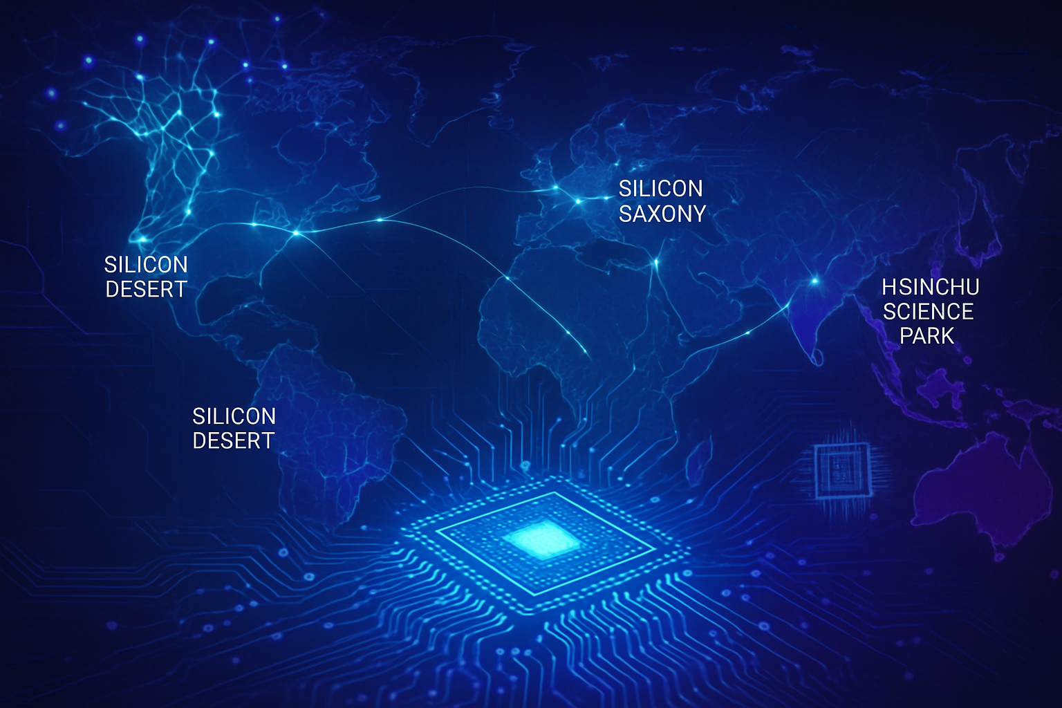
    The global semiconductor industry, a cornerstone of modern technology, is undergoing a profound transformation, and at its heart lies a less-heralded but critically important innovation: advanced ceramic components. As the relentless march towards miniaturization and enhanced performance continues, these specialized materials are proving indispensable, enabling the intricate and demanding processes required for cutting-edge chip manufacturing. The market for semiconductor ceramic components is experiencing robust growth, with projections indicating a significant expansion over the next decade, underscoring their fundamental importance in shaping the future of electronics.

    Driven by an insatiable demand for more powerful and efficient electronic devices, from advanced smartphones to artificial intelligence accelerators and electric vehicles, the semiconductor ceramic components market is poised to exceed US$3 billion by 2027 for consumable parts alone, with broader market segments reaching well over US$7 billion by 2032. This surge reflects the materials' unique ability to withstand the extreme temperatures, aggressive chemicals, and precise environments inherent in fabricating chips at the nanometer scale. Far from being mere commodities, these ceramics are critical enablers, ensuring the reliability, precision, and performance that define the next era of semiconductor technology.

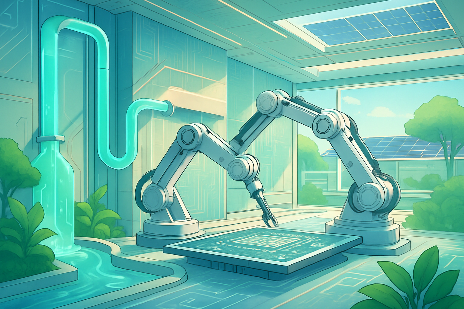
    The Unseen Architecture: Precision Engineering with Advanced Ceramics

    The intricate world of semiconductor manufacturing relies on materials that can perform under the most unforgiving conditions, and advanced ceramics are rising to this challenge. A diverse array of ceramic materials, each with tailored properties, is employed across various stages of chip fabrication, addressing limitations that traditional materials simply cannot overcome.

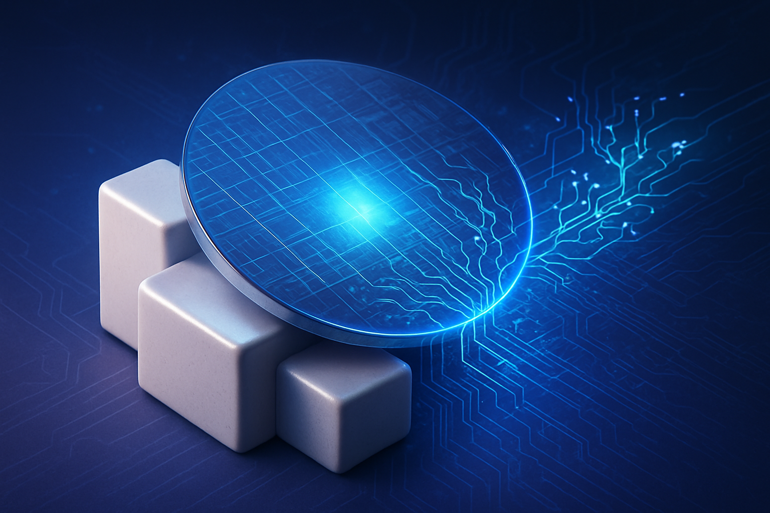
    Key ceramic materials include alumina (Al₂O₃), widely used for its excellent electrical insulation, high hardness, and chemical resistance, making it suitable for structural components, insulators, and substrates. Silicon carbide (SiC) stands out for its extreme hardness, high thermal conductivity, and chemical inertness, crucial for plasma etching equipment, wafer carriers, and high-temperature furnace components. Aluminum nitride (AlN) is prized for its exceptional thermal conductivity combined with good electrical insulation, making it ideal for heat sinks, substrates in power electronics, and high-frequency applications where efficient heat dissipation is paramount. Yttria (Y₂O₃), often used as a coating, offers superior plasma resistance, particularly against fluorine-based plasmas, extending the lifespan of critical process chamber components. Other specialized ceramics like silicon nitride (Si₃N₄) and zirconia (ZrO₂) also find niches due to their mechanical strength, wear resistance, and toughness.

    These advanced ceramics fundamentally differ from traditional materials like metals, plastics, and glass in several critical ways. Metals, while conductive, can contaminate highly sensitive processes, corrode under aggressive chemistries, and suffer from thermal expansion that compromises precision. Plastics lack the high-temperature resistance, chemical inertness, and dimensional stability required for wafer processing. Glass, while offering some chemical resistance, is typically brittle and lacks the mechanical strength and thermal properties needed for demanding equipment parts. Ceramics, in contrast, offer an unparalleled combination of properties: exceptional purity to prevent contamination, superior resistance to aggressive plasma gases and corrosive chemicals, remarkable dimensional stability across extreme temperature fluctuations, high mechanical strength and hardness for precision parts, and tailored electrical and thermal properties for specific applications. They are instrumental in overcoming technical challenges such as plasma erosion, thermal stress, chemical attack, and the need for ultra-high precision in environments where layers are measured in mere nanometers.

    Initial reactions from the AI research community and industry experts emphasize the symbiotic relationship between material science and semiconductor advancements. The ability to precisely control material properties at the atomic level allows for the creation of components that not only survive but thrive in the harsh environments of advanced fabrication. Experts highlight that without these specialized ceramics, the continued scaling of Moore's Law and the development of next-generation AI hardware, which demands ever-denser and more efficient chips, would be severely hampered. The focus on high-purity, ultra-dense ceramics with controlled microstructures is a testament to the continuous innovation in this crucial segment.

    Corporate Beneficiaries and Competitive Edge in a Ceramic-Driven Market

    The escalating reliance on advanced ceramic components is reshaping the competitive landscape within the semiconductor industry, creating significant opportunities for specialized materials companies and influencing the strategies of major chip manufacturers and equipment providers.

    Companies specializing in advanced ceramics and precision engineering stand to benefit immensely from this development. Key players in this market include Kyocera Corporation (TYO: 6971), a Japanese multinational ceramics and electronics manufacturer renowned for its wide range of ceramic components for semiconductor equipment, including fine ceramics for wafer processing and packaging. CoorsTek, Inc., a privately held global leader in engineered ceramics, provides high-performance ceramic solutions for etch, deposition, and other critical semiconductor processes. Morgan Advanced Materials plc (LSE: MGAM), a UK-based engineering company, offers advanced ceramic products and systems crucial for thermal management and high-temperature applications in semiconductor manufacturing. Other significant contributors include Hitachi Metals, Ltd. (TYO: 5486), Showa Denko K.K. (TYO: 4004), NGK Insulators, Ltd. (TYO: 5333), and Shin-Etsu Chemical Co., Ltd. (TYO: 4063), all of whom are investing heavily in R&D and manufacturing capabilities for these specialized materials.

    The competitive implications for major AI labs and tech giants are substantial. While they may not directly produce these components, their ability to innovate in chip design and AI hardware is directly tied to the availability and performance of advanced ceramic parts. Companies like Intel Corporation (NASDAQ: INTC), Taiwan Semiconductor Manufacturing Company (TSMC) (NYSE: TSM), and Samsung Electronics Co., Ltd. (KRX: 005930) rely heavily on their equipment suppliers—who, in turn, rely on ceramic component manufacturers—to push the boundaries of fabrication. Strategic partnerships and long-term supply agreements with leading ceramic producers are becoming increasingly vital to secure access to these critical materials, ensuring smooth production cycles and enabling the adoption of advanced manufacturing nodes.

    This development also poses a potential disruption to existing products or services that may not be optimized for the extreme conditions enabled by advanced ceramics. Equipment manufacturers that fail to integrate these superior materials into their designs risk falling behind competitors who can offer more robust, precise, and efficient fabrication tools. The market positioning for ceramic suppliers is strengthening, as their expertise becomes a strategic advantage. Companies that can innovate in ceramic material science, offering higher purity, better plasma resistance, or enhanced thermal properties, gain a significant competitive edge. This drives a continuous cycle of innovation, where advancements in material science directly fuel breakthroughs in semiconductor technology, ultimately benefiting the entire tech ecosystem.

    Wider Significance: Enabling the AI Era and Beyond

    The ascendance of advanced ceramic components in semiconductor manufacturing is not merely a technical footnote; it represents a pivotal trend within the broader AI and technology landscape, underpinning the foundational capabilities required for future innovation. Their significance extends far beyond the factory floor, impacting the performance, efficiency, and sustainability of the digital world.

    This trend fits squarely into the broader AI landscape and ongoing technological shifts. The proliferation of AI, machine learning, and high-performance computing (HPC) demands increasingly complex and powerful processors. These advanced chips, whether for training sophisticated neural networks or deploying AI at the edge, require manufacturing processes that push the limits of physics and chemistry. Ceramic components enable these processes by providing the stable, pure, and extreme-condition-resistant environments necessary for fabricating chips with billions of transistors. Without them, the continued scaling of computational power, which is the engine of AI progress, would face insurmountable material limitations.

    The impacts are far-reaching. On one hand, advanced ceramics contribute to the relentless pursuit of Moore's Law, allowing for smaller, faster, and more energy-efficient chips. This, in turn, fuels innovation in areas like autonomous vehicles, medical diagnostics, quantum computing, and sustainable energy solutions, all of which depend on sophisticated semiconductor technology. On the other hand, there are potential concerns. The specialized nature of these materials and the intricate manufacturing processes involved could lead to supply chain vulnerabilities if production is concentrated in a few regions or companies. Geopolitical tensions, as seen in recent years, could exacerbate these issues, highlighting the need for diversified sourcing and robust supply chain resilience.

    Comparing this development to previous AI milestones reveals its foundational role. While breakthroughs in AI algorithms (e.g., deep learning, transformer architectures) capture headlines, the underlying hardware advancements, enabled by materials like advanced ceramics, are equally critical. Just as the invention of the transistor and the development of silicon purification were foundational milestones, the continuous refinement and application of advanced materials in fabrication are essential for sustaining the pace of innovation. This is not a singular breakthrough but an ongoing evolution in material science that continuously raises the ceiling for what AI hardware can achieve.

    The Horizon: Future Developments and Uncharted Territories

    The journey of advanced ceramic components in semiconductor manufacturing is far from over, with experts predicting a future characterized by even greater material sophistication and integration, driven by the insatiable demands of emerging technologies.

    In the near term, we can expect continued refinement of existing ceramic materials, focusing on enhancing purity, improving plasma erosion resistance, and optimizing thermal management properties. Research is actively exploring novel ceramic composites and coatings that can withstand even more aggressive plasma chemistries and higher temperatures as chip features shrink further into the sub-3nm realm. Long-term developments are likely to involve the integration of AI and machine learning into ceramic material design and manufacturing processes, enabling accelerated discovery of new materials with tailored properties and more efficient production. Additive manufacturing (3D printing) of complex ceramic parts is also on the horizon, promising greater design flexibility and faster prototyping for semiconductor equipment.

    However, challenges remain. The cost of developing and manufacturing these highly specialized ceramics can be substantial, potentially impacting the overall cost of semiconductor production. Ensuring consistent quality and purity across large-scale manufacturing remains a technical hurdle. Furthermore, the industry will need to address sustainability concerns related to the energy-intensive production of some ceramic materials and the responsible disposal or recycling of components at the end of their lifecycle. Experts predict a future where material science becomes an even more central pillar of semiconductor innovation, with cross-disciplinary collaboration between material scientists, process engineers, and chip designers becoming the norm. The emphasis will be on "smart ceramics" that can self-monitor or even adapt to changing process conditions.

    A Foundational Pillar for the AI-Driven Future

    The growth and significance of the semiconductor ceramic components market represent a quiet but profound revolution at the heart of the digital age. These specialized materials are not merely incremental improvements; they are foundational enablers, critically supporting the relentless advancements in chip manufacturing that power everything from our everyday devices to the most sophisticated AI systems.

    The key takeaway is clear: without the unique properties of advanced ceramics—their unparalleled resistance to extreme conditions, their dimensional stability, and their tailored electrical and thermal characteristics—the current pace of semiconductor innovation would be impossible. They are the unsung heroes facilitating the miniaturization, performance enhancement, and reliability that define modern integrated circuits. This development's significance in AI history cannot be overstated; it underpins the hardware infrastructure upon which all algorithmic and software breakthroughs are built. It's a testament to the symbiotic relationship between material science and computational progress.

    Looking ahead, the long-term impact of this ceramic revolution will be the continued acceleration of technological progress across all sectors that rely on advanced electronics. As AI becomes more pervasive, demanding ever-more powerful and efficient processing, the role of these materials will only grow. What to watch for in the coming weeks and months includes further announcements of strategic partnerships between ceramic manufacturers and semiconductor equipment suppliers, new material innovations designed for sub-2nm process nodes, and increased investment in sustainable manufacturing practices for these critical components. The future of AI, in many ways, is being forged in the high-purity crucibles where advanced ceramics are born.

    This content is intended for informational purposes only and represents analysis of current AI developments.

    TokenRing AI delivers enterprise-grade solutions for multi-agent AI workflow orchestration, AI-powered development tools, and seamless remote collaboration platforms.
    For more information, visit https://www.tokenring.ai/.

  • Silicon’s Green Revolution: Semiconductor Giants Forge a Sustainable Future

    Silicon’s Green Revolution: Semiconductor Giants Forge a Sustainable Future

    The relentless march of technological progress, powered by the semiconductor industry, has long come with a significant environmental footprint. However, a seismic shift is underway as leading chip manufacturers worldwide are increasingly prioritizing eco-friendly production and robust environmental initiatives. Driven by escalating regulatory pressures, burgeoning consumer and investor demand for corporate responsibility, and the undeniable imperative to mitigate climate change, the industry is embarking on a green revolution, fundamentally reshaping how the world's most critical components are made. This pivot towards sustainability is not merely a public relations exercise but a strategic imperative, promising to redefine operational efficiency, supply chain resilience, and long-term viability for an industry at the heart of the global economy.

    This comprehensive move towards greener manufacturing encompasses ambitious targets for renewable energy adoption, revolutionary advancements in water conservation, aggressive waste reduction strategies, and the development of more sustainable materials and processes. From landmark power purchase agreements to cutting-edge wastewater treatment technologies, companies are investing heavily in innovations that promise to drastically reduce their carbon emissions, water consumption, and hazardous waste generation. The immediate significance of these efforts is profound, signaling a rapid acceleration towards a more environmentally conscious industrial landscape and setting new benchmarks for corporate sustainability in high-tech manufacturing.

    Engineering a Greener Chip: Technical Breakthroughs in Sustainable Manufacturing

    The semiconductor industry's pivot towards sustainability is underpinned by a series of significant technical advancements and strategic shifts in manufacturing practices. These initiatives represent a stark departure from previous, less environmentally conscious approaches, focusing on resource optimization, emission reduction, and circular economy principles.

    A cornerstone of this transformation is the aggressive pursuit of renewable energy integration. Historically, semiconductor fabs have been massive energy consumers, relying heavily on grid electricity often generated from fossil fuels. Modern initiatives involve direct investment in renewable energy sources and large-scale power purchase agreements (PPAs). For instance, Taiwan Semiconductor Manufacturing Company (TSMC) (TWSE: 2330, NYSE: TSM) made headlines in February 2024 by securing the world's largest corporate renewable energy PPA for an offshore wind farm, aiming to cover 25% of its electricity needs by 2026. This move, along with its accelerated goal for 100% renewable energy by 2040, signifies a strategic shift from simply offsetting emissions to directly powering operations with clean energy. This differs from older methods that might have focused on energy efficiency within the fab, but not necessarily on the source of the energy itself. Initial reactions from environmental advocacy groups have been largely positive, hailing these agreements as critical steps towards decarbonizing a notoriously energy-intensive sector.

    Water conservation and recycling represent another critical technical frontier. Semiconductor manufacturing demands vast quantities of ultrapure water (UPW) for cleaning silicon wafers, a process that traditionally led to significant wastewater discharge. New technologies are dramatically altering this paradigm. GlobalFoundries (NASDAQ: GFS), for example, announced in March 2024 a breakthrough wastewater treatment technology achieving a 98% recycling rate for process water. This advanced multi-stage filtration and purification system goes far beyond conventional wastewater treatment, which might only make water suitable for non-industrial uses, by rendering it pure enough for re-entry into sensitive fabrication processes. This drastically reduces reliance on fresh water sources and minimizes discharge. Similarly, Intel Corporation (NASDAQ: INTC) already treats and returns approximately 80% of its used water to surrounding communities, showcasing advanced treatment capabilities. These efforts are crucial in mitigating the industry's impact on local water supplies, particularly in drought-prone regions where many fabs are located.

    Waste reduction and the adoption of circular economy principles are also gaining significant technical traction. The industry traditionally generated substantial hazardous waste, including spent chemicals, solvents, and e-waste. Current efforts focus on "green chemistry" – developing and utilizing less hazardous materials and processes – and advanced recycling. Brewer Science, for instance, has maintained Zero Waste GreenCircle Certification for six consecutive years through its Green Chemistry Program, which identifies sustainable chemical alternatives and diverts hazardous materials for reuse. This involves sophisticated chemical recovery systems and material segregation at the source, a significant improvement over simple disposal. Furthermore, research is intensifying into recovering valuable materials from end-of-life chips, moving away from linear "take-make-dispose" models towards a more cyclical approach. Industry experts emphasize that these technical shifts are not just about compliance but about innovating new processes that are inherently more sustainable and resource-efficient.

    Finally, energy-efficient chip design and smart manufacturing are playing a pivotal role. While not directly about fab operations, designing chips that consume less power throughout their lifecycle significantly reduces the overall energy footprint of electronics. NVIDIA Corporation (NASDAQ: NVDA), with its Blackwell Hopper series of GPUs announced in March 2024, claims to offer 25 times less energy consumption for certain workloads, demonstrating how design-level innovations contribute to sustainability. Concurrently, the integration of AI and machine learning into manufacturing processes (smart manufacturing) is optimizing resource usage in real-time, predicting equipment failures, and fine-tuning chemical flows to reduce waste and energy consumption. This data-driven approach allows for precision not achievable with traditional, less automated production lines, leading to tangible reductions in energy, water, and chemical use on the factory floor.

    Competitive Edge: How Sustainability Shapes the Semiconductor Landscape

    The escalating focus on sustainable practices is profoundly impacting semiconductor companies, creating new competitive dynamics, strategic advantages, and potential disruptions across the industry. Companies that proactively embrace and excel in environmental initiatives are positioning themselves for long-term success, while those lagging may face significant challenges.

    Major players like TSMC (TWSE: 2330, NYSE: TSM), Intel Corporation (NASDAQ: INTC), and GlobalFoundries (NASDAQ: GFS) stand to benefit significantly from their ambitious sustainability commitments. By investing heavily in renewable energy, water recycling, and waste reduction, these giants are not only mitigating environmental risks but also enhancing their brand reputation and attracting a growing pool of environmentally conscious investors. Their substantial capital expenditure in green technologies, such as TSMC's record-breaking renewable energy PPA or GlobalFoundries' 98% water recycling breakthrough, can translate into significant operational cost savings over time through reduced energy bills and lower resource consumption. This financial benefit, coupled with improved ESG (Environmental, Social, and Governance) ratings, makes them more attractive to institutional investors who increasingly integrate sustainability criteria into their investment decisions.

    The competitive implications are far-reaching. For major foundries, a strong sustainability profile can become a key differentiator when securing contracts from major tech companies (like Apple, Qualcomm, or NVIDIA) that have their own stringent supply chain sustainability requirements. Companies with demonstrably greener manufacturing processes may gain preferential treatment, potentially shifting market share. This creates pressure on smaller players or those with less mature sustainability programs to catch up, requiring substantial investment in R&D and infrastructure. Moreover, the adoption of advanced water recycling or energy-efficient processes can reduce vulnerability to resource scarcity and volatile energy prices, offering a strategic advantage in regions prone to environmental stresses.

    Potential disruption to existing products or services might not be immediate, but the long-term shift is undeniable. Companies that fail to adapt could face increased regulatory scrutiny, higher operating costs due to carbon taxes or water levies, and reputational damage. This could make their products less competitive in a market that increasingly values ethical and sustainable sourcing. Conversely, companies like NVIDIA Corporation (NASDAQ: NVDA), by designing energy-efficient chips such as the Blackwell Hopper series, are not only addressing a critical environmental concern (data center energy consumption) but also creating a product with a compelling performance-per-watt advantage, which is a powerful market differentiator. This illustrates how sustainability can drive product innovation and create new market opportunities rather than just being a cost center.

    In terms of market positioning, companies leading in sustainability are establishing themselves as industry pioneers and responsible corporate citizens. This can attract top talent, foster innovation, and build stronger relationships with governments and local communities. For example, Infineon Technologies AG (FSE: IFX, OTCQX: IFNNY), with its goal for carbon neutrality by 2030, is demonstrating a commitment that resonates with a global workforce and customer base. This strategic advantage extends beyond direct manufacturing, influencing the entire semiconductor ecosystem, from materials suppliers to equipment manufacturers (like ASML Holding N.V. (NASDAQ: ASML)), who are increasingly being pushed by their customers to develop more sustainable solutions and supply chains. The drive for sustainability is thus becoming a non-negotiable aspect of competitive viability and market leadership in the semiconductor sector.

    Beyond the Fab: Wider Implications for AI and the Global Landscape

    The semiconductor industry's concerted push towards sustainable practices carries profound wider significance, resonating across the broader technological landscape, influencing global environmental trends, and impacting the future of artificial intelligence. This shift is not an isolated phenomenon but an integral part of a larger global movement towards sustainable development and climate resilience.

    This fits squarely into the broader AI landscape and trends by addressing the growing environmental footprint of AI itself. As AI models become more complex and data centers expand exponentially, the energy demands for training and running these systems skyrocket. The chips manufactured today are the bedrock of tomorrow's AI. Therefore, if the production of these foundational components becomes greener, it directly contributes to a more sustainable AI ecosystem. Companies like NVIDIA Corporation (NASDAQ: NVDA) are not only building chips for AI but also designing them to be significantly more energy-efficient, acknowledging that the energy consumption of AI hardware is a critical concern. This symbiotic relationship means that advancements in semiconductor sustainability are crucial for enabling the responsible growth of AI and mitigating its environmental impact.

    The impacts extend far beyond the industry itself. Environmentally conscious semiconductor manufacturing directly contributes to global climate change mitigation efforts by reducing greenhouse gas emissions, conserving precious water resources, and minimizing hazardous waste. As the foundational technology for nearly all modern electronics, a greener semiconductor supply chain means that the devices consumers use—from smartphones to electric vehicles—have a lower embedded carbon footprint. This empowers consumers to make more sustainable choices and pushes brands relying on these chips to adopt more responsible sourcing practices. Furthermore, the innovations developed within the semiconductor sector for water treatment, energy efficiency, and chemical recycling can potentially be transferred and applied to other heavy industries, creating a ripple effect of positive environmental change.

    However, potential concerns and challenges remain. The cost of implementing advanced green technologies can be substantial, potentially leading to higher production costs, at least in the short term. There's also the challenge of standardizing sustainability metrics and reporting across a globally interconnected and complex supply chain, ensuring genuine progress rather than "greenwashing." The industry's reliance on certain rare earth minerals and other raw materials, often sourced from regions with questionable environmental and labor practices, also presents an ongoing ethical and sustainability challenge that requires continuous vigilance and improvement in supply chain transparency.

    Comparisons to previous AI milestones and breakthroughs highlight the evolving nature of technological responsibility. While past milestones focused purely on performance and capability, the current era demands an integration of performance with planetary stewardship. This marks a maturity in the tech industry where environmental impact is no longer an afterthought but a core design and manufacturing principle. This commitment to sustainability in semiconductors is as critical as any performance breakthrough, as it ensures the long-term viability of the technology itself within planetary boundaries.

    The Horizon of Green Silicon: Future Developments and Expert Predictions

    The journey towards a fully sustainable semiconductor industry is ongoing, with significant developments expected in the near-term and long-term. The confluence of technological innovation, regulatory evolution, and shifting market demands will continue to drive profound changes.

    In the near term, we can anticipate a rapid acceleration in the adoption of advanced water reclamation and zero-liquid discharge (ZLD) systems. As water scarcity intensifies globally, fabs will increasingly move towards closed-loop water systems, minimizing their reliance on municipal supplies. Experts predict that AI and machine learning will play an even greater role in optimizing these complex water treatment processes, ensuring maximum efficiency and purity. Furthermore, the integration of more robust renewable energy solutions will continue, with more companies following TSMC's lead in large-scale PPAs and potentially investing directly in solar or wind farms adjacent to their facilities. There will also be a stronger push for sustainable packaging solutions for chips, moving away from plastics towards biodegradable or recycled materials.

    Looking further ahead, the long-term developments will likely center on revolutionary materials science and process engineering. This includes research into entirely new etching and deposition techniques that require fewer hazardous chemicals or less energy. The development of "green" solvents and photoresists that are biodegradable or easily recyclable will become paramount. Experts foresee a future where the entire lifecycle of a semiconductor, from raw material extraction to end-of-life recycling, is meticulously designed for minimal environmental impact. This could involve advanced urban mining techniques to recover precious metals from e-waste, creating a truly circular economy for silicon. There's also potential for carbon capture and utilization (CCU) technologies to be integrated into fab operations, capturing potent greenhouse gases like NF3 and converting them into inert or useful substances.

    However, several challenges need to be addressed. The primary challenge remains the cost-effectiveness of implementing cutting-edge green technologies at scale without compromising the competitive pricing of chips. Standardization of environmental impact assessments across the diverse global supply chain is also crucial to ensure transparent and comparable reporting. Furthermore, the industry will need to navigate the complexities of global regulatory fragmentation, as different regions adopt varying environmental standards and carbon pricing mechanisms.

    What experts predict will happen next is a continued, intensified focus on collaboration across the supply chain. Chip manufacturers will exert greater pressure on their equipment and materials suppliers to innovate greener solutions. Initiatives like the International Electronics Manufacturing Initiative's (iNEMI) Life Cycle Assessment (LCA) framework will become standardized, providing a holistic view of environmental impact. The semiconductor industry is poised to become a benchmark for sustainable manufacturing, demonstrating that high-tech innovation and environmental stewardship can, and must, go hand in hand.

    Silicon's Sustainable Leap: A Landmark Moment for Tech and Planet

    The semiconductor industry is at a pivotal juncture, undergoing a transformative shift towards sustainable practices that promises to redefine its future and significantly impact the global environmental landscape. The comprehensive efforts detailed—from monumental commitments to renewable energy and revolutionary water recycling technologies to aggressive waste reduction and energy-efficient chip designs—underscore a profound recognition of environmental responsibility as a core business imperative.

    The key takeaways from this green revolution are clear: sustainability is no longer an optional add-on but a strategic differentiator and a driver of innovation. Major players like TSMC, Intel, GlobalFoundries, and NVIDIA are not just reacting to regulatory pressures but proactively investing in technologies and processes that enhance efficiency, reduce risk, and build long-term resilience. These initiatives demonstrate that economic growth and environmental stewardship can be mutually reinforcing, leading to both financial benefits and enhanced brand value in an increasingly conscious market.

    This development's significance in AI history, though indirectly, is immense. As the foundational technology for artificial intelligence, a greener semiconductor industry lays the groundwork for a more sustainable AI future, mitigating the environmental footprint of increasingly powerful and energy-intensive AI systems. It represents a maturation of the tech sector, where the pursuit of cutting-edge performance is now inextricably linked with the responsibility to protect the planet. This commitment sets a powerful precedent for other high-tech industries.

    In the coming weeks and months, observers should watch for continued announcements of large-scale renewable energy deals, further breakthroughs in water and chemical recycling, and the emergence of new industry standards for environmental reporting and supply chain transparency. The push for more sustainable materials and manufacturing processes will intensify, driven by both internal R&D and external stakeholder demands. The semiconductor industry's green leap is a testament to its capacity for innovation, not just in performance, but in its profound commitment to a sustainable future for technology and for the planet.

    This content is intended for informational purposes only and represents analysis of current AI developments.

    TokenRing AI delivers enterprise-grade solutions for multi-agent AI workflow orchestration, AI-powered development tools, and seamless remote collaboration platforms.
    For more information, visit https://www.tokenring.ai/.

  • The New Silicon Curtain: Geopolitics Reshapes the Global Semiconductor Landscape

    The New Silicon Curtain: Geopolitics Reshapes the Global Semiconductor Landscape

    The global semiconductor industry, the bedrock of modern technology and the engine of the AI revolution, finds itself at the epicenter of an escalating geopolitical maelstrom. Driven primarily by intensifying US-China tensions, the once seamlessly interconnected supply chain is rapidly fracturing, ushering in an era of technological nationalism, restricted access, and a fervent race for self-sufficiency. This "chip war" is not merely a trade dispute; it's a fundamental realignment of power dynamics, with profound implications for innovation, economic stability, and the future trajectory of artificial intelligence.

    The immediate significance of this geopolitical tug-of-war is a profound restructuring of global supply chains, marked by increased costs, delays, and a concerted push towards diversification and reshoring. Nations and corporations alike are grappling with the imperative to mitigate risks associated with over-reliance on specific regions, particularly China. Concurrently, stringent export controls imposed by the United States aim to throttle China's access to advanced chip technologies, manufacturing equipment, and software, directly impacting its ambitions in cutting-edge AI and military applications. In response, Beijing is accelerating its drive for domestic technological independence, pouring vast resources into indigenous research and development, setting the stage for a bifurcated technological ecosystem.

    The Geopolitical Chessboard: Policies, Restrictions, and the Race for Independence

    The current geopolitical climate has spurred a flurry of policy actions and strategic maneuvers, fundamentally altering the landscape of semiconductor production and access. At the heart of the matter are the US export controls, designed to limit China's ability to develop advanced AI and military capabilities by denying access to critical semiconductor technologies. These measures include bans on the sale of cutting-edge Graphics Processing Units (GPUs) from companies like Nvidia (NASDAQ: NVDA) and Advanced Micro Devices (NASDAQ: AMD), crucial for AI training, as well as equipment necessary for producing chips smaller than 14 or 16 nanometers. The US has also expanded its Entity List, adding numerous Chinese tech firms and prohibiting US persons from supporting advanced Chinese chip facilities.

    These actions represent a significant departure from previous approaches, which largely favored an open, globally integrated semiconductor market. Historically, the industry thrived on international collaboration, with specialized firms across different nations contributing to various stages of chip design, manufacturing, and assembly. The new paradigm, however, emphasizes national security and technological decoupling, prioritizing strategic control over economic efficiency. This shift has ignited a vigorous debate within the AI research community and industry, with some experts warning of stifled innovation due to reduced collaboration and market fragmentation, while others argue for the necessity of securing critical supply chains and preventing technology transfer that could be used for adversarial purposes.

    China's response has been equally assertive, focusing on accelerating its "Made in China 2025" initiative, with an intensified focus on achieving self-sufficiency in advanced semiconductors. Billions of dollars in government subsidies and incentives are being channeled into domestic research, development, and manufacturing capabilities. This includes mandates for domestic companies to prioritize local AI chips over foreign alternatives, even reportedly instructing major tech companies to halt purchases of Nvidia's China-tailored GPUs. This aggressive pursuit of indigenous capacity aims to insulate China from foreign restrictions and establish its own robust, self-reliant semiconductor ecosystem, effectively creating a parallel technological sphere. The long-term implications of this bifurcated development path—one driven by Western alliances and the other by Chinese national imperatives—are expected to manifest in divergent technological standards, incompatible hardware, and a potential slowdown in global AI progress as innovation becomes increasingly siloed.

    Corporate Crossroads: Navigating the New Semiconductor Order

    The escalating geopolitical tensions are creating a complex and often challenging environment for AI companies, tech giants, and startups alike. Major semiconductor manufacturers such as Taiwan Semiconductor Manufacturing Company (NYSE: TSM) and Intel (NASDAQ: INTC) are at the forefront of this transformation. TSMC, a critical foundry for many of the world's leading chip designers, is investing heavily in new fabrication plants in the United States and Europe, driven by government incentives and the imperative to diversify its manufacturing footprint away from Taiwan, a geopolitical flashpoint. Similarly, Intel is aggressively pursuing its IDM 2.0 strategy, aiming to re-establish its leadership in foundry services and boost domestic production in the US and Europe, thereby benefiting from significant government subsidies like the CHIPS Act.

    For American AI companies, particularly those specializing in advanced AI accelerators and data center solutions, the US export controls present a double-edged sword. While the intent is to protect national security interests, companies like Nvidia (NASDAQ: NVDA) and AMD (NASDAQ: AMD) have faced significant revenue losses from restricted sales to the lucrative Chinese market. These companies are now forced to develop modified, less powerful versions of their chips for China, or explore alternative markets, impacting their competitive positioning and potentially slowing their overall R&D investment in the most advanced technologies. Conversely, Chinese AI chip startups, backed by substantial government funding, stand to benefit from the domestic push, gaining preferential access to the vast Chinese market and accelerating their development cycles in a protected environment.

    The competitive implications are profound. Major AI labs and tech companies globally are reassessing their supply chains, seeking resilience over pure cost efficiency. This involves exploring multiple suppliers, investing in proprietary chip design capabilities, and even co-investing in new fabrication facilities. For instance, hyperscalers like Google (NASDAQ: GOOGL), Amazon (NASDAQ: AMZN), and Microsoft (NASDAQ: MSFT) are increasingly designing their own custom AI chips (TPUs, Inferentia, Azure Maia AI Accelerator, respectively) to reduce reliance on external vendors and gain strategic control over their AI infrastructure. This trend could disrupt traditional chip vendor relationships and create new strategic advantages for companies with robust in-house silicon expertise. Startups, on the other hand, might face increased barriers to entry due to higher component costs and fragmented supply chains, making it more challenging to compete with established players who can leverage economies of scale and direct government support.

    The Broader Canvas: AI's Geopolitical Reckoning

    The geopolitical reshaping of the semiconductor industry fits squarely into a broader trend of technological nationalism and strategic competition, often dubbed an "AI Cold War." Control over advanced chips is no longer just an economic advantage; it is now explicitly viewed as a critical national security asset, essential for both military superiority and economic dominance in the age of AI. This shift underscores a fundamental re-evaluation of globalization, where the pursuit of interconnectedness is giving way to the imperative of technological sovereignty. The impacts are far-reaching, influencing everything from the pace of AI innovation to the very architecture of future digital economies.

    One of the most significant impacts is the potential for a divergence in AI development pathways. As the US and China develop increasingly independent semiconductor ecosystems, their respective AI industries may evolve along distinct technical standards, hardware platforms, and even ethical frameworks. This could lead to interoperability challenges and a fragmentation of the global AI research landscape, potentially slowing down universal advancements. Concerns also abound regarding the equitable distribution of AI benefits, as nations with less advanced domestic chipmaking capabilities could fall further behind, exacerbating the digital divide. The risk of technology weaponization also looms large, with advanced AI chips being central to autonomous weapons systems and sophisticated surveillance technologies.

    Comparing this to previous AI milestones, such as the rise of deep learning or the development of large language models, the current situation represents a different kind of inflection point. While past milestones were primarily driven by scientific breakthroughs and computational advancements, this moment is defined by geopolitical forces dictating the very infrastructure upon which AI is built. It's less about a new algorithm and more about who gets to build and control the engines that run those algorithms. The emphasis has shifted from pure innovation to strategic resilience and national security, making the semiconductor supply chain a critical battleground in the global race for AI supremacy. The implications extend beyond technology, touching on international relations, economic policy, and the very fabric of global cooperation.

    The Road Ahead: Future Developments and Uncharted Territory

    Looking ahead, the geopolitical impact on the semiconductor industry is expected to intensify, with several key developments on the horizon. In the near term, we can anticipate continued aggressive investment in domestic chip manufacturing capabilities by both the US and its allies, as well as China. The US CHIPS Act, along with similar initiatives in Europe and Japan, will likely fuel the construction of new fabs, though bringing these online and achieving significant production volumes will take years. Concurrently, China will likely double down on its indigenous R&D efforts, potentially achieving breakthroughs in less advanced but strategically vital chip technologies, and focusing on improving its domestic equipment manufacturing capabilities.

    Longer-term developments include the potential for a more deeply bifurcated global semiconductor market, where distinct ecosystems cater to different geopolitical blocs. This could lead to the emergence of two separate sets of standards and supply chains, impacting everything from consumer electronics to advanced AI infrastructure. Potential applications on the horizon include a greater emphasis on "trusted" supply chains, where the origin and integrity of every component are meticulously tracked, particularly for critical infrastructure and defense applications. We might also see a surge in innovative packaging technologies and chiplet architectures as a way to circumvent some manufacturing bottlenecks and achieve performance gains without relying solely on leading-edge fabrication.

    However, significant challenges need to be addressed. The enormous capital expenditure and technical expertise required to build and operate advanced fabs mean that true technological independence is a monumental task for any single nation. Talent acquisition and retention will be critical, as will fostering vibrant domestic innovation ecosystems. Experts predict a protracted period of strategic competition, with continued export controls, subsidies, and retaliatory measures. The possibility of unintended consequences, such as global chip oversupply in certain segments or a slowdown in the pace of overall technological advancement due to reduced collaboration, remains a significant concern. The coming years will be crucial in determining whether the world moves towards a more resilient, diversified, albeit fragmented, semiconductor industry, or if the current tensions escalate into a full-blown technological decoupling with far-reaching implications.

    A New Dawn for Silicon: Resilience in a Fragmented World

    In summary, the geopolitical landscape has irrevocably reshaped the semiconductor industry, transforming it from a globally integrated network into a battleground for technological supremacy. Key takeaways include the rapid fragmentation of supply chains, driven by US export controls and China's relentless pursuit of self-sufficiency. This has led to massive investments in domestic chipmaking by the US and its allies, while simultaneously spurring China to accelerate its indigenous R&D. The immediate significance lies in increased costs, supply chain disruptions, and a shift towards strategic resilience over pure economic efficiency.

    This development marks a pivotal moment in AI history, underscoring that the future of artificial intelligence is not solely dependent on algorithmic breakthroughs but also on the geopolitical control of its foundational hardware. It represents a departure from the idealized vision of a seamlessly globalized tech industry towards a more nationalistically driven, and potentially fragmented, future. The long-term impact could be a bifurcated technological world, with distinct AI ecosystems and standards emerging, posing challenges for global interoperability and collaborative innovation.

    In the coming weeks and months, observers should closely watch for further policy announcements from major governments, particularly regarding export controls and investment incentives. The progress of new fab constructions in the US and Europe, as well as China's advancements in domestic chip production, will be critical indicators of how this new silicon curtain continues to unfold. The reactions of major semiconductor players and their strategic adjustments will also offer valuable insights into the industry's ability to adapt and innovate amidst unprecedented geopolitical pressures.

    This content is intended for informational purposes only and represents analysis of current AI developments.

    TokenRing AI delivers enterprise-grade solutions for multi-agent AI workflow orchestration, AI-powered development tools, and seamless remote collaboration platforms.
    For more information, visit https://www.tokenring.ai/.

  • Google Unveils Next-Gen AI Silicon: Ironwood TPU and Tensor G5 Set to Reshape Cloud and Mobile AI Landscapes

    Google Unveils Next-Gen AI Silicon: Ironwood TPU and Tensor G5 Set to Reshape Cloud and Mobile AI Landscapes

    In a strategic double-strike against the escalating demands of artificial intelligence, Google (NASDAQ: GOOGL) has officially unveiled its latest custom-designed AI chips in 2025: the Ironwood Tensor Processing Unit (TPU) for powering its expansive cloud AI workloads and the Tensor G5, engineered to bring cutting-edge AI directly to its Pixel devices. These announcements, made at Google Cloud Next in April and the Made by Google event in August, respectively, signal a profound commitment by the tech giant to vertical integration and specialized hardware, aiming to redefine performance, energy efficiency, and competitive dynamics across the entire AI ecosystem.

    The twin chip unveilings underscore Google's aggressive push to optimize its AI infrastructure from the data center to the palm of your hand. With the Ironwood TPU, Google is arming its cloud with unprecedented processing power, particularly for the burgeoning inference needs of large language models (LLMs), while the Tensor G5 promises to unlock deeply integrated, on-device generative AI experiences for millions of Pixel users. This dual-pronged approach is poised to accelerate the development and deployment of next-generation AI applications, setting new benchmarks for intelligent systems globally.

    A Deep Dive into Google's Custom AI Engines: Ironwood TPU and Tensor G5

    Google's seventh-generation Ironwood Tensor Processing Unit (TPU), showcased at Google Cloud Next 2025, represents a pivotal advancement, primarily optimized for AI inference workloads—a segment projected to outpace training growth significantly in the coming years. Designed to meet the immense computational requirements of "thinking models" that generate proactive insights, Ironwood is built to handle the demands of LLMs and Mixture of Experts (MoEs) with unparalleled efficiency and scale.

    Technically, Ironwood TPUs boast impressive specifications. A single pod can scale up to an astounding 9,216 liquid-cooled chips, collectively delivering 42.5 Exaflops of compute power, a figure that reportedly surpasses the world's largest supercomputers in AI-specific tasks. This iteration offers a 5x increase in peak compute capacity over its predecessor, Trillium, coupled with 6x more High Bandwidth Memory (HBM) capacity (192 GB per chip) and 4.5x greater HBM bandwidth (7.37 TB/s per chip). Furthermore, Ironwood achieves a 2x improvement in performance per watt, making it nearly 30 times more power efficient than Google's inaugural Cloud TPU from 2018. Architecturally, Ironwood features a single primary compute die, likely fabricated on TSMC's N3P process with CoWoS packaging, and is Google's first multiple compute chiplet die, housing two Ironwood compute dies per chip. The system leverages a 3D Torus topology and breakthrough Inter-Chip Interconnect (ICI) networking for high density and minimal latency, all integrated within Google's Cloud AI Hypercomputer architecture and the Pathways software stack.

    Concurrently, the Tensor G5, debuting with the Pixel 10 series at the Made by Google event in August 2025, marks a significant strategic shift for Google's smartphone silicon. This chip is a custom design from scratch by Google and is manufactured by Taiwan Semiconductor Manufacturing Company (TSMC) (NYSE: TSM) using their advanced 3nm N3E process. This move away from Samsung, who manufactured previous Tensor chips, is expected to yield substantial efficiency improvements and enhanced battery life. The Tensor G5 is described as the most significant upgrade since the original Tensor, delivering snappy performance and enabling deeply helpful, on-device generative AI experiences powered by the newest Gemini Nano model. Initial benchmarks indicate a promising 73% increase in CPU multi-core performance over its predecessor and a 16% overall improvement in AnTuTu scores. The 8-core chipset features 1x Cortex-X4 at 3.78 GHz, 5x Cortex-A725 at 3.05 GHz, and 2x Cortex-A520 at 2.25 GHz, powering advanced AI features like "Magic Cue" for proactive in-app assistance and "Pro Res Zoom" for high-detail imagery.

    Reshaping the AI Industry: Competitive Implications and Strategic Advantages

    Google's unveiling of Ironwood TPU and Tensor G5 carries profound implications for the AI industry, poised to reshape competitive landscapes and strategic advantages for tech giants, AI labs, and even startups. The most direct beneficiary is undoubtedly Google (NASDAQ: GOOGL) itself, which gains unprecedented control over its AI hardware-software stack, allowing for highly optimized performance and efficiency across its cloud services and consumer devices. This vertical integration strengthens Google's position in the fiercely competitive cloud AI market and provides a unique selling proposition for its Pixel smartphone lineup.

    The Ironwood TPU directly challenges established leaders in the cloud AI accelerator market, most notably NVIDIA (NASDAQ: NVDA), whose GPUs have long dominated AI training and inference. By offering a scalable, highly efficient, and cost-effective alternative specifically tailored for inference workloads, Ironwood could disrupt NVIDIA's market share, particularly for large-scale deployments of LLMs in the cloud. This increased competition is likely to spur further innovation from all players, potentially leading to a more diverse and competitive AI hardware ecosystem. For AI companies and startups, the availability of Ironwood through Google Cloud could democratize access to cutting-edge AI processing, enabling them to deploy more sophisticated models without the prohibitive costs of building their own specialized infrastructure.

    The Tensor G5 intensifies competition in the mobile silicon space, directly impacting rivals like Qualcomm (NASDAQ: QCOM) and Apple (NASDAQ: AAPL), which also design custom chips for their flagship devices. Google's shift to TSMC (NYSE: TSM) for manufacturing signals a desire for greater control over performance and efficiency, potentially setting a new bar for on-device AI capabilities. This could pressure other smartphone manufacturers to accelerate their own custom silicon development or to seek more advanced foundry services. The Tensor G5's ability to run advanced generative AI models like Gemini Nano directly on-device could disrupt existing services that rely heavily on cloud processing for AI features, offering enhanced privacy, speed, and offline functionality to Pixel users. This strategic move solidifies Google's market positioning as a leader in both cloud and edge AI.

    The Broader AI Landscape: Trends, Impacts, and Concerns

    Google's 2025 AI chip unveilings—Ironwood TPU and Tensor G5—are not isolated events but rather integral pieces of a broader, accelerating trend within the AI landscape: the relentless pursuit of specialized hardware for optimized AI performance and efficiency. This development significantly reinforces the industry's pivot towards vertical integration, where leading tech companies are designing their silicon to tightly integrate with their software stacks and AI models. This approach, pioneered by companies like Apple, is now a crucial differentiator in the AI race, allowing for unprecedented levels of optimization that general-purpose hardware often cannot match.

    The impact of these chips extends far beyond Google's immediate ecosystem. Ironwood's focus on inference for large-scale cloud AI is a direct response to the explosion of generative AI and LLMs, which demand immense computational power for deployment. By making such power more accessible and efficient through Google Cloud, it accelerates the adoption and practical application of these transformative models across various industries, from advanced customer service bots to complex scientific simulations. Simultaneously, the Tensor G5's capabilities bring sophisticated on-device generative AI to the masses, pushing the boundaries of what smartphones can do. This move empowers users with more private, responsive, and personalized AI experiences, reducing reliance on constant cloud connectivity and opening doors for innovative offline AI applications.

    However, this rapid advancement also raises potential concerns. The increasing complexity and specialization of AI hardware could contribute to a widening "AI divide," where companies with the resources to design and manufacture custom silicon gain a significant competitive advantage, potentially marginalizing those reliant on off-the-shelf solutions. There are also environmental implications, as even highly efficient chips contribute to the energy demands of large-scale AI, necessitating continued innovation in sustainable computing. Comparisons to previous AI milestones, such as the initial breakthroughs in deep learning with GPUs, show a consistent pattern: specialized hardware is key to unlocking the next generation of AI capabilities, and Google's latest chips are a clear continuation of this trajectory, pushing the envelope of what's possible at both the cloud and edge.

    The Road Ahead: Future Developments and Expert Predictions

    The unveiling of Ironwood TPU and Tensor G5 marks a significant milestone, but it is merely a waypoint on the rapidly evolving journey of AI hardware. In the near term, we can expect Google (NASDAQ: GOOGL) to aggressively roll out Ironwood TPUs to its Google Cloud customers, focusing on demonstrating tangible performance and cost-efficiency benefits for large-scale AI inference workloads, particularly for generative AI models. The company will likely showcase new developer tools and services that leverage Ironwood's unique capabilities, further enticing businesses to migrate or expand their AI operations on Google Cloud. For Pixel devices, the Tensor G5 will be the foundation for a suite of enhanced, on-device AI features, with future software updates likely unlocking even more sophisticated generative AI experiences, potentially extending beyond current "Magic Cue" and "Pro Res Zoom" functionalities.

    Looking further ahead, experts predict a continued escalation in the "AI chip arms race." The success of Ironwood and Tensor G5 will likely spur even greater investment from Google and its competitors into custom silicon development. We can anticipate future generations of TPUs and Tensor chips that push the boundaries of compute density, memory bandwidth, and energy efficiency, possibly incorporating novel architectural designs and advanced packaging technologies. Potential applications and use cases on the horizon include highly personalized, proactive AI assistants that anticipate user needs, real-time multimodal AI processing directly on devices, and even more complex, context-aware generative AI that can operate with minimal latency.

    However, several challenges need to be addressed. The increasing complexity of chip design and manufacturing, coupled with global supply chain volatilities, poses significant hurdles. Furthermore, ensuring the ethical and responsible deployment of increasingly powerful on-device AI, particularly concerning privacy and potential biases, will be paramount. Experts predict that the next wave of innovation will not only be in raw processing power but also in the seamless integration of hardware, software, and AI models, creating truly intelligent and adaptive systems. The focus will shift towards making AI not just powerful, but also ubiquitous, intuitive, and inherently helpful, setting the stage for a new era of human-computer interaction.

    A New Era for AI: Google's Hardware Gambit and Its Lasting Impact

    Google's (NASDAQ: GOOGL) 2025 unveiling of the Ironwood Tensor Processing Unit (TPU) for cloud AI and the Tensor G5 for Pixel devices represents a monumental strategic move, solidifying the company's commitment to owning the full stack of AI innovation, from foundational hardware to end-user experience. The key takeaways from this announcement are clear: Google is doubling down on specialized AI silicon, not just for its massive cloud infrastructure but also for delivering cutting-edge, on-device intelligence directly to consumers. This dual-pronged approach positions Google as a formidable competitor in both the enterprise AI and consumer electronics markets, leveraging custom hardware for unparalleled performance and efficiency.

    This development holds immense significance in AI history, marking a decisive shift towards vertical integration as a competitive imperative in the age of generative AI. Just as the advent of GPUs catalyzed the deep learning revolution, these custom chips are poised to accelerate the next wave of AI breakthroughs, particularly in inference and on-device intelligence. The Ironwood TPU's sheer scale and efficiency for cloud inference, coupled with the Tensor G5's ability to bring sophisticated AI to mobile, collectively set new benchmarks for what is technologically feasible. This move underscores a broader industry trend where companies like Google are taking greater control over their hardware destiny to unlock unique AI capabilities that off-the-shelf components simply cannot provide.

    Looking ahead, the long-term impact of Ironwood and Tensor G5 will likely be measured by how effectively they democratize access to advanced AI, accelerate the development of new applications, and ultimately reshape user interactions with technology. We should watch for the widespread adoption of Ironwood in Google Cloud, observing how it influences the cost and performance of deploying large-scale AI models for businesses. On the consumer front, the evolution of Pixel's AI features, powered by the Tensor G5, will be a critical indicator of how deeply integrated and useful on-device generative AI can become in our daily lives. The coming weeks and months will reveal the initial market reactions and real-world performance metrics, providing further insights into how these custom chips will truly redefine the future of artificial intelligence.

    This content is intended for informational purposes only and represents analysis of current AI developments.

    TokenRing AI delivers enterprise-grade solutions for multi-agent AI workflow orchestration, AI-powered development tools, and seamless remote collaboration platforms.
    For more information, visit https://www.tokenring.ai/.

  • The Green Revolution in Silicon: Semiconductor Industry Forges a Sustainable Future

    The Green Revolution in Silicon: Semiconductor Industry Forges a Sustainable Future

    The semiconductor industry, the foundational bedrock of our digital world, is embarking on a profound transformation to reconcile its immense technological contributions with its significant environmental footprint. As the global demand for advanced chips—especially those powering the burgeoning field of Artificial Intelligence—continues its exponential ascent, the urgency for sustainable manufacturing practices has reached a critical inflection point. This shift is not merely a regulatory compliance exercise but a strategic imperative, driven by escalating energy demands, mounting environmental scrutiny, and a commitment to reducing the industry's overall ecological impact.

    This green revolution in silicon manufacturing signifies a concerted effort to integrate energy efficiency, reduce environmental harm, and implement cutting-edge green technologies across every stage of chip production. From sourcing raw materials to the intricate fabrication processes within multi-billion-dollar fabs, companies are redefining what it means to produce the brains of modern technology responsibly. This immediate and impactful pivot is crucial for ecological preservation and vital for the industry's economic resilience, regulatory adherence, and continued innovation in an increasingly environmentally conscious global technology landscape.

    Engineering a Greener Chip: Technical Advancements and Eco-Conscious Production

    The pursuit of sustainability in semiconductor manufacturing is catalyzing a wave of groundbreaking technical advancements and the widespread adoption of green technologies, marking a significant departure from older, more resource-intensive production methods. At the heart of this transformation are innovations aimed at drastically reducing energy consumption, conserving water, minimizing chemical waste, and abating greenhouse gas emissions.

    A primary focus is renewable energy integration and overall energy efficiency. Fabrication plants (fabs) are aggressively transitioning to powering their operations with renewable sources like solar and wind. Companies like Intel (NASDAQ: INTC) have committed to 100% renewable electricity across their global operations by 2030, while Taiwan Semiconductor Manufacturing Company (NYSE: TSM) has advanced its RE100 goal to 2040. Beyond sourcing, "green fabs" are being designed with optimized infrastructure, advanced HVAC systems, and energy-efficient equipment. Process-level efficiencies are also critical, with advancements like Extreme Ultraviolet (EUV) lithography being optimized to reduce energy per wafer. Notably, TSMC's "EUV Dynamic Energy Saving Program," launched in September 2025, has already demonstrated a 44% reduction in peak power consumption of EUV tools, projected to save 190 million kilowatt-hours (kWh) of electricity and cut carbon emissions by 101 kilotons by 2030. Furthermore, the adoption of advanced materials like Gallium Nitride (GaN) and Silicon Carbide (SiC) offers superior energy efficiency in power electronics compared to traditional silicon. AI and machine learning (ML) are also being deployed to optimize manufacturing processes, enabling precise control over resource usage and reducing energy consumption by up to 30% in idle tools.

    Water reclamation and conservation represent another critical area of innovation. Semiconductor fabs require immense volumes of ultrapure water, making water scarcity a growing concern. Manufacturers are implementing sophisticated multi-stage recycling systems, including advanced Reverse Osmosis (RO) filtration and electro-deionization (EDI), to treat and reuse process water, achieving high recycling rates. For instance, GlobalFoundries has announced a breakthrough wastewater treatment technology achieving a 98% recycling rate. Intel, for its part, restored over 2 billion gallons of water to local communities in 2022 and aims for net-positive water by 2030. These closed-loop systems and optimization efforts contrast sharply with older methods that often involved significant fresh water intake and less efficient wastewater management.

    In terms of green chemistry and emissions reduction, the industry is tackling the challenge of fluorinated gases (F-GHGs), potent greenhouse gases used in etching and chamber cleaning. Strategies include optimizing production processes, switching to alternative input gases, and installing advanced abatement systems to detoxify exhaust gases. Samsung (KRX: 005930) developed a Regenerative Catalytic System (RCS) that achieves up to 95% processing efficiency for greenhouse gas emissions. Companies are also moving towards substituting hazardous chemicals with more environmentally friendly alternatives. The shift from older methods, which often released a significant percentage of unreacted gases into the atmosphere, to these precise control and abatement systems is a substantial leap forward. Finally, waste reduction and circular economy principles are gaining traction, with efforts in silicon and chemical recycling, sustainable packaging, and promoting product life extension to minimize electronic waste. Lam Research (NASDAQ: LRCX), for example, has introduced technologies like Lam Cryo™ 3.0, which delivers a projected 40% reduction in energy consumption per wafer and cuts process gas emissions by approximately 90%, and utilizes virtual twin technology to reduce emissions by up to 80% by replacing physical experimentation with digital simulation. These integrated sustainability approaches contrast with past practices where environmental concerns were often an afterthought, showcasing a fundamental re-engineering of the entire manufacturing ethos.

    Reshaping the Tech Landscape: Industry Impact and Competitive Dynamics

    The accelerating drive towards sustainability in semiconductor manufacturing is sending ripples across the entire tech industry, fundamentally altering competitive landscapes, influencing product development, and creating new strategic advantages for companies ranging from AI innovators to established tech giants and agile startups.

    Tech giants such as Apple (NASDAQ: AAPL), Google (NASDAQ: GOOGL), Microsoft (NASDAQ: MSFT), and Amazon (NASDAQ: AMZN) are at the forefront of demanding more sustainable practices from their semiconductor suppliers. Many have committed to ambitious net-zero emissions goals, with deadlines approaching (e.g., Apple aiming for carbon-neutral silicon production by 2030). This translates into rigorous supply chain requirements, pushing chipmakers to accelerate their green initiatives. Companies that can deliver energy-efficient, sustainably produced chips stand to benefit immensely, securing lucrative contracts and strengthening partnerships with these influential buyers. This competitive pressure encourages major semiconductor manufacturers like TSMC, Intel, and Samsung to invest heavily in sustainable fabs and processes, positioning them as leaders and attracting environmentally conscious customers.

    For AI companies, the relationship with semiconductor sustainability is dual-edged. The explosive growth of AI fuels an insatiable demand for computational power, leading to a surge in energy consumption, particularly in data centers. TechInsights forecasts a staggering 300% increase in CO2 emissions from AI accelerators alone between 2025 and 2029, highlighting the urgent need for sustainable solutions. This puts pressure on AI firms to prioritize energy-efficient chip designs and optimize data center operations. Conversely, AI itself is emerging as a powerful tool for achieving sustainability in semiconductor manufacturing, optimizing processes, reducing waste, and enabling predictive maintenance. Companies that leverage AI for sustainable design and manufacturing, alongside developing inherently energy-efficient AI chips (e.g., Google's TPUs), will gain a significant competitive edge by reducing operational costs and appealing to a growing segment of environmentally aware customers and investors.

    Startups, while facing high barriers to entry in the semiconductor space, are finding vast opportunities in niche areas of sustainable innovation. Initiatives like "Startups for Sustainable Semiconductors (S3)" are connecting climate tech startups with corporate venture capitalists, fostering innovation in areas such as advanced cooling technologies, sustainable materials, chemical recovery, PFAS destruction, and AI-driven energy management. These agile innovators can disrupt existing products and services by offering greener alternatives for production processes, energy-efficient equipment, or materials with lower environmental impact. The shift towards circular design principles—products designed for reuse, repair, and easier material recovery—will also challenge traditional "take-make-dispose" models, favoring companies that embrace product longevity and resource efficiency. Overall, sustainability is no longer just a compliance issue; it's a strategic differentiator that will redefine market positioning and reward companies that proactively integrate environmental responsibility into their core business models.

    AI's Green Imperative: Broader Significance and Evolving Landscape

    The drive for sustainability in semiconductor manufacturing holds profound wider significance, particularly as it intersects with the burgeoning Artificial Intelligence landscape. This convergence highlights both the environmental challenges posed by AI's rapid expansion and the critical role of sustainable chip production in mitigating these impacts, shaping the future trajectory of technology itself.

    The semiconductor industry’s environmental footprint is substantial. In 2020, the sector emitted approximately 64.24 million tons of CO2-equivalent gases, with energy consumption in fabs comparable to small cities. The demand for ultrapure water runs into millions of gallons daily, and the use of hazardous chemicals like perfluorocarbons (PFCs), potent greenhouse gases, contributes significantly to pollution. The "AI Gold Rush" exacerbates these issues, as AI's "insatiable hunger" for computational power directly translates into increased demand for chips, further straining resources. Data centers, the backbone of AI, are projected to triple their power consumption by 2030, with AI workloads consuming 10 to 30 times more electricity than traditional computing tasks. This unprecedented scale of demand, projected to push the global semiconductor market to $800 billion in 2025, positions semiconductor sustainability as a paramount concern for the entire digital ecosystem.

    However, this heightened environmental awareness also presents potential concerns. The high cost of transitioning to greener production processes, involving substantial initial capital investments, can be an obstacle. The sheer complexity of chip production, with over 300 individual steps, makes it challenging for outside innovators to introduce sustainable solutions. Regulatory conflicts, such as restrictions on certain chemicals (e.g., PFAS bans) used in manufacturing, can create tension between economic security and sustainability objectives. Despite these challenges, the current focus on sustainability represents a significant evolution from previous tech milestones. While past technological advancements also increased energy consumption, the current urgency is driven by a global climate crisis, with policymakers and customers now prioritizing ecological concerns alongside supply security—a marked shift from earlier eras where environmental impact was often an afterthought.

    This push for green manufacturing aligns with broader AI trends, where the technology itself is becoming a solution to the very problems it exacerbates. AI and Machine Learning are pivotal in optimizing resource usage, designing energy-efficient chips, and streamlining manufacturing processes. This dual nature—AI as both a driver of demand and a tool for sustainability—underscores its critical role in shaping a more responsible technological future. The industry is actively pursuing solutions such as green hydrogen adoption, advanced water reclamation systems, eco-friendly material usage, and circular economy practices, all of which are increasingly informed and optimized by AI. This integrated approach, where sustainability is embedded into core design and operational philosophies, marks a new era for technology development, demanding a balance between innovation and environmental responsibility.

    The Horizon of Green Silicon: Future Developments and Expert Outlook

    The journey towards a fully sustainable semiconductor industry is a long-term endeavor, but the trajectory of future developments points towards a deeply integrated and technologically advanced approach to environmental stewardship. Both near-term and long-term trends indicate a profound reshaping of how chips are designed, manufactured, and utilized.

    In the near term (1-5 years), the industry will see an accelerated integration of renewable energy, with major chipmakers like Intel (NASDAQ: INTC) targeting 100% renewable electricity by 2030, and TSMC (NYSE: TSM) aiming for 25% from renewable sources by the same year. Water conservation will remain a critical focus, with advanced reclamation systems becoming standard, potentially mandated by stricter regulations such as those proposed by the European Union. Expect to see continued emphasis on sustainable material sourcing and the adoption of "green chemistry," replacing hazardous chemicals and optimizing gas usage. Efforts to reduce "Scope 3" emissions—indirect emissions from the supply chain—will also intensify as companies seek to holistically address their environmental footprint.

    Looking further into the long term (5-10+ years), the industry is poised for more transformative changes to achieve ambitious net-zero and carbon-neutral goals by 2050. This will involve significant R&D into novel, sustainable materials beyond traditional silicon, such as organic semiconductors and perovskites, to enable even more energy-efficient AI. Wide-bandgap materials like Gallium Nitride (GaN) and Silicon Carbide (SiC) will become more prevalent, especially in power electronics for electric vehicles and renewable energy systems. The full realization of circular economy principles will see chips designed for disassembly, and advanced recycling methods for critical raw material recovery will become standard practice. Experts predict the increasing integration of green hydrogen for fabrication processes and the potential for nuclear-powered systems to meet the immense energy demands of future AI-driven fabs. Smart manufacturing, leveraging end-to-end digitalization, AI, and machine learning, will be crucial for optimizing every aspect of production, from energy and water consumption to yield and quality control.

    The potential applications of these sustainable semiconductor advancements are vast. They will be integral to electric vehicles (EVs), enhancing efficiency in charging and motor control. They will power more efficient renewable energy systems (solar cells, smart grids) and drastically reduce energy consumption in data centers and cloud computing. Crucially, innovations like organic semiconductors promise significantly lower power consumption for AI accelerators and edge computing devices, enabling more distributed and sustainable AI deployments. However, significant challenges persist, including the high energy consumption of advanced nodes, massive water usage, the continued reliance on hazardous chemicals, and the growing volume of e-waste. The complexity of global supply chains also makes it difficult to track and reduce Scope 3 emissions effectively. Experts like Michael Luciano from Jama Software anticipate continued research into novel materials and refined processes, with AI playing a pivotal role in optimizing designs, modeling energy consumption, and managing resources in real-time. The future hinges on a collaborative, innovative, and adaptive approach, balancing technological advancement with environmental responsibility.

    The Dawn of Sustainable AI: A Comprehensive Wrap-Up

    The semiconductor industry stands at a critical juncture, where the relentless march of technological innovation, particularly in Artificial Intelligence, must be harmonized with an unwavering commitment to environmental stewardship. This comprehensive review underscores that sustainability in semiconductor manufacturing is not a peripheral concern but a foundational imperative, reshaping the very essence of how our digital future is built.

    The key takeaways are clear: the semiconductor sector, while indispensable, is inherently resource-intensive, demanding vast quantities of energy, water, and chemicals, leading to significant greenhouse gas emissions. The exponential growth of AI exacerbates these environmental challenges, with AI accelerators alone projected to cause a 300% increase in CO2 emissions between 2025 and 2029. However, the industry is responding with a robust "green revolution," driven by increasing climate awareness, stringent regulations, investor demands, and the economic benefits of efficiency. Leading companies are making ambitious commitments to net-zero emissions and 100% renewable energy, underpinned by innovations in advanced water reclamation, circular economy practices, green chemistry, energy-efficient chip design, and the transformative power of AI and machine learning in optimizing every aspect of production.

    The significance of this development in AI history is profound and dual-faceted. On one hand, AI's insatiable hunger for computational power presents a formidable environmental challenge, extending its carbon footprint from operational phases to its very genesis in semiconductor fabs. Without "greener silicon," the full transformative promise of AI could be overshadowed by its escalating ecological cost. Conversely, AI itself is emerging as an indispensable tool for achieving sustainability within semiconductor manufacturing, enabling precise control, optimizing resource utilization, and driving the design of more efficient processes. This symbiotic relationship underscores that sustainable chip production is not merely an ethical consideration but a foundational requirement for the long-term viability and ethical development of AI itself.

    Looking at the long-term impact, sustainability is transcending its role as mere compliance, evolving into a primary driver of innovation, competitiveness, and new revenue streams. Green manufacturing practices are expected to significantly reduce operational costs, bolstering economic viability. Achieving these ambitious goals will necessitate unprecedented global collaboration across the entire value chain, fostering a more circular economy model where design for longevity, repairability, and material reuse becomes standard. Further research into novel, sustainable materials beyond silicon, such as organic semiconductors and wide-bandgap materials, will enable even more energy-efficient AI and power electronics.

    What to watch for in the coming weeks and months includes the formal details and funding allocations from initiatives like the CHIPS for America program, alongside new legislation such as the EU's proposed stricter water usage regulations for semiconductor fabs. Keep an eye on accelerated corporate sustainability commitments from top semiconductor companies, particularly regarding net-zero targets and renewable energy adoption. Monitor technological breakthroughs in green hydrogen integration, advanced water recycling, and the development of new eco-friendly materials. Crucially, observe the expanding role of AI and machine learning in optimizing manufacturing processes and designing more energy-efficient chips, while simultaneously tracking the energy consumption trends of AI accelerators to gauge the effectiveness of mitigation strategies. Progress in industry-wide standardization efforts and increased supply chain transparency will also be key indicators of the industry's commitment to a truly sustainable future. The dawn of sustainable AI is upon us, and its evolution will be one of the most compelling narratives of the coming decades.

    This content is intended for informational purposes only and represents analysis of current AI developments.

    TokenRing AI delivers enterprise-grade solutions for multi-agent AI workflow orchestration, AI-powered development tools, and seamless remote collaboration platforms.
    For more information, visit https://www.tokenring.ai/.

  • Malaysia’s Tech Frontier: How TVET is Forging a Skilled Workforce for the Semiconductor and AI Revolution

    Malaysia’s Tech Frontier: How TVET is Forging a Skilled Workforce for the Semiconductor and AI Revolution

    Malaysia is strategically leveraging Technical and Vocational Education and Training (TVET) to cultivate a robust and skilled workforce, essential for driving its high-growth semiconductor and Artificial Intelligence (AI) industries. These concerted efforts are immediately significant, aiming to cement Malaysia's position as a regional technology hub and ensure sustainable economic competitiveness in the era of Industry 4.0 and beyond. By prioritizing hands-on training and competency-based learning, TVET programs are indispensable for bridging talent gaps and equipping the workforce with practical, industry-relevant skills and knowledge, directly enhancing employability and contributing significantly to the nation's economic development.

    The nation's focused investment in TVET for these critical sectors is a strategic move to meet surging global demand for advanced chips, fueled by generative AI, the Internet of Things (IoT), and electric vehicles (EVs). This initiative positions Malaysia to expand its role beyond traditional assembly and testing into higher value-chain activities like design, research, and engineering services, fostering a virtuous cycle where AI drives new applications for semiconductors, and semiconductor advancements enable more sophisticated AI solutions.

    Cultivating a Future-Ready Workforce: Malaysia's Strategic TVET Blueprint

    Malaysia's commitment to developing a highly skilled workforce for its high-growth semiconductor and AI industries is underpinned by a comprehensive and multi-faceted TVET blueprint. This strategy is explicitly outlined in key national frameworks such as the National Semiconductor Strategy (NSS), the National TVET Policy 2030, and the New Industrial Master Plan 2030 (NIMP 2030), all of which aim to foster high-value industries through a robust talent pipeline. Unlike traditional academic pathways, TVET programs are meticulously designed to provide practical, industry-specific skills, ensuring graduates are immediately employable and capable of contributing to cutting-edge technological advancements.

    The government's dedication is further evidenced by significant budgetary allocations. Budget 2026 prioritizes the cultivation of highly skilled talent in AI and upstream semiconductor industries, building on the RM6.8 billion allocated for TVET development programs in Budget 2024, with an additional RM200 million recently approved. The 2025 national budget dedicates MYR1 billion towards talent development, specifically supporting universities and high-value projects in IC design services and advanced material development. These funds facilitate the establishment and enhancement of specialized programs and academies tailored to the needs of the semiconductor and AI sectors.

    Key initiatives include the Semiconductor Technology Academy-Department of Manpower (STAc-JTM), launched to produce highly skilled human capital for the high-tech industry, and the TVET Place & Train UTeM@KPT programme, which strategically aligns educational outcomes with industry demands, particularly in semiconductor manufacturing. The Malaysia Automotive Robotics and Internet of Things Institute (MARii) is establishing dedicated digital hubs to develop expertise in data analytics, robotics, and AI. Furthermore, the Engineering Talent for Semiconductor Industry programme provides structured internships and targeted training. These programs emphasize hands-on learning, simulations, and real-world projects, differing significantly from theoretical academic models by focusing on immediate application and problem-solving within an industrial context.

    Crucially, there is a strong emphasis on robust partnerships between educational institutions and industries to ensure skill development is relevant and timely. Multinational corporations like Micron Malaysia (NASDAQ: MU) are actively investing in workforce development through curriculum partnerships, national certification schemes, and internal AI upskilling programs. They also engage in R&D collaborations with local universities and support initiatives like Chip Camp Malaysia. Similarly, AMD (NASDAQ: AMD) has inaugurated a state-of-the-art R&D center in Penang, focusing on AI PC, server data center, and data center GPU development, collaborating with local firms, academia, and government to upskill the workforce. Penang's proactive STEM talent blueprint and efforts to strengthen capabilities in Automatic Testing Equipment (ATE) further underscore regional commitment, complemented by initiatives like Collaborative Research in Engineering, Science, and Technology (CREST) which fosters strong collaboration between academic institutions, government agencies, and private companies.

    Corporate Beneficiaries and Competitive Implications

    Malaysia's aggressive push in TVET for semiconductor and AI skills presents a significant boon for both established tech giants and emerging startups looking to expand or establish operations in Southeast Asia. Companies like Infineon Technologies (ETR: IFX), Nvidia (NASDAQ: NVDA), Google (NASDAQ: GOOGL), Micron Technology (NASDAQ: MU), and AMD (NASDAQ: AMD) stand to benefit immensely from a readily available pool of highly skilled local talent. These global players are increasingly investing in Malaysia, drawn by its established semiconductor ecosystem and the promise of a future-ready workforce capable of handling advanced manufacturing, IC design, and AI development. For instance, Micron Malaysia's and AMD's investments in local workforce development and R&D centers directly leverage and contribute to this growing talent pool.

    The competitive implications for major AI labs and tech companies are substantial. A robust TVET pipeline reduces reliance on expatriate talent, lowers operational costs, and fosters a more stable and localized workforce. This can give Malaysia a strategic advantage in attracting foreign direct investment (FDI) over other regional competitors. For companies like Nvidia, which are at the forefront of AI hardware and software, having access to engineers and technicians skilled in advanced packaging, testing, and AI system integration in Malaysia can accelerate their product development cycles and enhance their supply chain resilience. The ability to quickly scale up operations with skilled local talent is a critical factor in the fast-paced AI and semiconductor industries.

    This development has the potential to disrupt existing products and services by enabling higher-value activities within Malaysia. As the TVET system churns out talent capable of IC design and advanced engineering, Malaysia can move beyond its traditional role in back-end assembly and testing. This shift could lead to more localized innovation, potentially fostering new startups and services that leverage Malaysia's growing expertise in areas like generative AI and specialized chip design. For tech giants, it means the potential for deeper integration of their R&D and manufacturing processes within Malaysia, creating more sophisticated regional hubs. Market positioning is enhanced for companies that strategically partner with Malaysian TVET institutions, gaining early access to graduates and influencing curriculum development to meet their specific technological needs.

    Broader Significance and Global Trends

    Malaysia's strategic investment in TVET for the semiconductor and AI sectors is not an isolated initiative but fits squarely into broader global trends emphasizing talent development for advanced manufacturing and digital economies. As nations worldwide grapple with the demands of Industry 4.0 and the accelerating pace of technological change, the ability to cultivate and retain a skilled workforce has become a critical determinant of national competitiveness. Malaysia's efforts mirror similar initiatives in countries like Germany, Singapore, and South Korea, which have long recognized the value of vocational training in supporting their high-tech industries. The nation's ambition to become a regional hub for deep-technology development and a generative AI hub by 2030 underscores its commitment to remaining relevant in the global technology landscape.

    The impacts of these initiatives are far-reaching. Economically, a skilled workforce attracts further foreign investment, stimulates local innovation, and enables Malaysia to climb the value chain from manufacturing to design and R&D, thereby securing higher economic returns and long-term resilience. Socially, it provides high-quality employment opportunities for Malaysian citizens, reduces youth unemployment, and helps destigmatize TVET as an equally viable and valuable career pathway compared to traditional academic routes. By training 60,000 highly skilled engineers for the semiconductor industry by 2030 and doubling STEM enrollment, Malaysia aims to reduce reliance on foreign talent and create a sustainable, homegrown talent ecosystem.

    Potential concerns, however, include the challenge of keeping TVET curricula updated with the incredibly rapid advancements in AI and semiconductor technologies. The pace of change necessitates constant re-evaluation and adaptation of training programs to prevent skills obsolescence. Furthermore, ensuring equitable access to quality TVET programs across all regions and demographics within Malaysia remains crucial. Comparisons to previous AI milestones highlight that the availability of skilled human capital is as critical as computational power or data in driving innovation. Just as the development of software engineers fueled the internet boom, a new generation of TVET-trained technicians and engineers will be essential for the widespread adoption and advancement of AI and next-generation semiconductors. Malaysia's proactive stance positions it to be a significant player in this evolving global narrative.

    Anticipating Future Developments and Challenges

    Looking ahead, Malaysia's TVET landscape for the semiconductor and AI industries is poised for significant near-term and long-term developments. In the near term, we can expect to see an accelerated rollout of specialized training modules, potentially leveraging virtual reality (VR) and augmented reality (AR) for more immersive and practical learning experiences. The focus will likely intensify on niche areas such as advanced packaging, chiplet technology, quantum computing hardware, and explainable AI (XAI) within the curriculum. There will also be an increased emphasis on micro-credentials and continuous upskilling programs to ensure the existing workforce remains competitive and adaptable to new technologies. The government's continued substantial budgetary allocations, such as the MYR1 billion in the 2025 national budget for talent development, will fuel these expansions.

    Potential applications and use cases on the horizon include the development of localized AI solutions tailored for Malaysian industries, from smart manufacturing in semiconductor fabs to AI-powered diagnostics in healthcare. We could also see Malaysia becoming a testbed for new semiconductor architectures designed for AI, driven by its skilled workforce and established infrastructure. Experts predict a further deepening of industry-academia collaboration, with more companies establishing dedicated training centers or co-developing programs with TVET institutions. The Prime Minister's call for streamlined and faster approval processes for new academic programs suggests a future where educational offerings can respond with unprecedented agility to industry demands.

    However, several challenges need to be addressed. The primary challenge remains the rapid evolution of technology; keeping TVET curricula and instructor expertise current with the bleeding edge of AI and semiconductor innovation will require continuous investment and proactive engagement with industry leaders. Attracting sufficient numbers of students into STEM and TVET fields, especially women, to meet the ambitious targets (e.g., 60,000 highly skilled engineers by 2030) will also be critical. Additionally, ensuring that TVET graduates possess not only technical skills but also critical thinking, problem-solving, and adaptability will be essential for long-term career success. Experts predict that the success of Malaysia's strategy will hinge on its ability to foster a culture of lifelong learning and innovation within its TVET ecosystem, ensuring that its workforce is not just skilled for today but ready for the technologies of tomorrow.

    A Blueprint for Global Tech Competitiveness

    Malaysia's comprehensive and proactive approach to Technical and Vocational Education and Training (TVET) stands as a pivotal blueprint for national competitiveness in the global technology arena. The concerted efforts to cultivate a highly skilled workforce for the high-growth semiconductor and AI industries represent a strategic investment in the nation's economic future. By focusing on practical, industry-relevant training, Malaysia is effectively bridging the talent gap, attracting significant foreign direct investment from global players like Micron (NASDAQ: MU) and AMD (NASDAQ: AMD), and positioning itself to move up the value chain from manufacturing to advanced design and R&D.

    This development is significant in AI history as it underscores the critical role of human capital development in realizing the full potential of artificial intelligence and advanced technologies. While breakthroughs in algorithms and hardware often grab headlines, the ability of a nation to train and deploy a skilled workforce capable of implementing, maintaining, and innovating with these technologies is equally, if not more, crucial for sustained growth and impact. Malaysia's strategy highlights that the "AI race" is not just about invention, but also about the effective cultivation of talent. The destigmatization of TVET and its elevation as an equally important pathway to high-tech careers is a crucial social and economic shift that other developing nations can emulate.

    In the coming weeks and months, observers should watch for further announcements regarding new industry partnerships, the launch of advanced TVET programs, and updates on the progress towards Malaysia's ambitious talent development targets. The success of these initiatives will not only determine Malaysia's standing as a regional tech hub but also offer valuable lessons for other countries striving to build a future-ready workforce in an increasingly technology-driven world. Malaysia's journey serves as a compelling case study on how strategic investment in vocational education can unlock national potential and drive significant advancements in critical high-growth industries.

    This content is intended for informational purposes only and represents analysis of current AI developments.

    TokenRing AI delivers enterprise-grade solutions for multi-agent AI workflow orchestration, AI-powered development tools, and seamless remote collaboration platforms.
    For more information, visit https://www.tokenring.ai/.

  • Google Unveils Ironwood TPU and Tensor G5: A Dual Assault on AI’s Next Frontier

    Google Unveils Ironwood TPU and Tensor G5: A Dual Assault on AI’s Next Frontier

    Google (NASDAQ: GOOGL) has ignited a new era in artificial intelligence hardware with the unveiling of its latest custom-designed AI chips in 2025: the Ironwood Tensor Processing Unit (TPU) for cloud AI workloads and the Tensor G5 for its flagship Pixel devices. These announcements, made at Cloud Next in April and the Made by Google event in August, respectively, signal a strategic and aggressive push by the tech giant to redefine performance, energy efficiency, and competitive dynamics across the entire AI ecosystem. With Ironwood squarely targeting large-scale AI inference in data centers and the Tensor G5 empowering next-generation on-device AI, Google is poised to significantly reshape how AI is developed, deployed, and experienced.

    The immediate significance of these chips cannot be overstated. Ironwood, Google's 7th-generation TPU, marks a pivotal shift by primarily optimizing for AI inference, a workload projected to outpace training growth by a factor of 12 by 2026. This move directly challenges the established market leaders like Nvidia (NASDAQ: NVDA) by offering a highly scalable and cost-effective solution for deploying AI at an unprecedented scale. Concurrently, the Tensor G5 solidifies Google's vertical integration strategy, embedding advanced AI capabilities directly into its hardware products, promising more personalized, efficient, and powerful experiences for users. Together, these chips underscore Google's comprehensive vision for AI, from the cloud's vast computational demands to the intimate, everyday interactions on personal devices.

    Technical Deep Dive: Inside Google's AI Silicon Innovations

    Google's Ironwood TPU, the 7th generation of its Tensor Processing Units, represents a monumental leap in specialized hardware, primarily designed for the burgeoning demands of large-scale AI inference. Unveiled at Cloud Next 2025, a full 9,216-chip Ironwood cluster boasts an astonishing 42.5 exaflops of AI compute, making it 24 times faster than the world's current top supercomputer. Each individual Ironwood chip delivers 4,614 teraflops of peak FP8 performance, signaling Google's aggressive intent to dominate the inference segment of the AI market.

    Technically, Ironwood is a marvel of engineering. It features a substantial 192GB of HBM3 (High Bandwidth Memory), a six-fold increase in capacity and 4.5 times more bandwidth (7.37 TB/s) compared to its predecessor, the Trillium TPU. This memory expansion is critical for handling the immense context windows and parameter counts of modern large language models (LLMs) and Mixture of Experts (MoE) architectures. Furthermore, Ironwood achieves a remarkable 2x better performance per watt than Trillium and is nearly 30 times more power-efficient than the first Cloud TPU from 2018, a testament to its advanced, likely sub-5nm manufacturing process and sophisticated liquid cooling solutions. Architectural innovations include an inference-first design optimized for low-latency and real-time applications, an enhanced Inter-Chip Interconnect (ICI) offering 1.2 TBps bidirectional bandwidth for seamless scaling across thousands of chips, improved SparseCore accelerators for embedding models, and native FP8 support for enhanced throughput.

    The AI research community and industry experts have largely hailed Ironwood as a transformative development. It's widely seen as Google's most direct and potent challenge to Nvidia's (NASDAQ: NVDA) long-standing dominance in the AI accelerator market, with some early performance comparisons reportedly suggesting Ironwood's capabilities rival or even surpass Nvidia's GB200 in certain performance-per-watt scenarios. Experts emphasize Ironwood's role in ushering in an "age of inference," enabling "thinking models" and proactive AI agents at an unprecedented scale, while its energy efficiency improvements are lauded as crucial for the sustainability of increasingly demanding AI workloads.

    Concurrently, the Tensor G5, Google's latest custom mobile System-on-a-Chip (SoC), is set to power the Pixel 10 series, marking a significant strategic shift. Manufactured by Taiwan Semiconductor Manufacturing Company (TSMC) (NYSE: TSM) using its cutting-edge 3nm process node, the Tensor G5 promises substantial gains over its predecessor. Google claims a 34% faster CPU and an NPU (Neural Processing Unit) that is up to 60% more powerful than the Tensor G4. This move to TSMC is particularly noteworthy, addressing previous concerns about efficiency and thermal management associated with earlier Tensor chips manufactured by Samsung (KRX: 005930).

    The Tensor G5's architectural innovations are heavily focused on enhancing on-device AI. Its next-generation TPU enables the chip to run the newest Gemini Nano model 2.6 times faster and 2 times more efficiently than the Tensor G4, expanding the token window from 12,000 to 32,000. This empowers advanced features like real-time voice translation, sophisticated computational photography (e.g., advanced segmentation, motion deblur, 10-bit HDR video, 100x AI-processed zoom), and proactive AI agents directly on the device. Improved thermal management, with graphite cooling in base models and vapor chambers in Pro variants, aims to sustain peak performance.

    Initial reactions to the Tensor G5 are more nuanced. While its vastly more powerful NPU and enhanced ISP are widely praised for delivering unprecedented on-device AI capabilities and a significantly improved Pixel experience, some industry observers have noted reservations regarding its raw CPU and particularly GPU performance. Early benchmarks suggest the Tensor G5's GPU may lag behind flagship offerings from rivals like Qualcomm (NASDAQ: QCOM) (Snapdragon 8 Elite) and Apple (NASDAQ: AAPL) (A18 Pro), and in some tests, even its own predecessor, the Tensor G4. The absence of ray tracing support for gaming has also been a point of criticism. However, experts generally acknowledge Google's philosophy with Tensor chips: prioritizing deeply integrated, AI-driven experiences and camera processing over raw, benchmark-topping CPU/GPU horsepower to differentiate its Pixel ecosystem.

    Industry Impact: Reshaping the AI Hardware Battleground

    Google's Ironwood TPU is poised to significantly reshape the competitive landscape of cloud AI, particularly for inference workloads. By bolstering Google Cloud's (NASDAQ: GOOGL) "AI Hypercomputer" architecture, Ironwood dramatically enhances the capabilities available to customers, enabling them to tackle the most demanding AI tasks with unprecedented performance and efficiency. Internally, these chips will supercharge Google's own vast array of AI services, from Search and YouTube recommendations to advanced DeepMind experiments. Crucially, Google is aggressively expanding the external supply of its TPUs, installing them in third-party data centers like FluidStack and offering financial guarantees to promote adoption, a clear strategic move to challenge the established order.

    This aggressive push directly impacts the major players in the AI hardware market. Nvidia (NASDAQ: NVDA), which currently holds a commanding lead in AI accelerators, faces its most formidable challenge yet, especially in the inference segment. While Nvidia's H100 and B200 GPUs remain powerful, Ironwood's specialized design and superior efficiency for LLMs and MoE models aim to erode Nvidia's market share. The move also intensifies pressure on AMD (NASDAQ: AMD) and Intel (NASDAQ: INTC), who are also vying for a larger slice of the specialized AI silicon pie. Among hyperscale cloud providers, the competition is heating up, with Amazon (NASDAQ: AMZN) (AWS Inferentia/Trainium) and Microsoft (NASDAQ: MSFT) (Azure Maia/Cobalt) similarly investing heavily in custom silicon to optimize their AI offerings and reduce reliance on third-party hardware.

    The disruptive potential of Ironwood extends beyond direct competition. Its specialized nature and remarkable efficiency for inference could accelerate a broader shift away from using general-purpose GPUs for certain AI deployment tasks, particularly in vast data centers where cost and power efficiency are paramount. The superior performance-per-watt could significantly lower the operational costs of running large AI models, potentially democratizing access to powerful AI inference for a wider range of companies and enabling entirely new types of AI-powered products and services that were previously too expensive or computationally intensive to deploy.

    On the mobile front, the Tensor G5 is set to democratize advanced on-device AI. With its vastly enhanced NPU, the G5 can run the powerful Gemini Nano model entirely on the device, fostering innovation for startups focused on privacy-preserving and offline AI. This creates new opportunities for developers to build next-generation mobile AI applications, leveraging Google's tightly integrated hardware and AI models.

    The Tensor G5 intensifies the rivalry in the premium smartphone market. Google's (NASDAQ: GOOGL) shift to TSMC's (NYSE: TSM) 3nm process positions the G5 as a more direct competitor to Apple's (NASDAQ: AAPL) A-series chips and their Neural Engine, with Google aiming for "iPhone-level SoC upgrades" and seeking to close the performance gap. Within the Android ecosystem, Qualcomm (NASDAQ: QCOM), the dominant supplier of premium SoCs, faces increased pressure. As Google's Tensor chips become more powerful and efficient, they enable Pixel phones to offer unique, AI-driven features that differentiate them, potentially making it harder for other Android OEMs relying on Qualcomm to compete directly on AI capabilities.

    Ultimately, both Ironwood and Tensor G5 solidify Google's strategic advantage through profound vertical integration. By designing both the chips and the AI software (like TensorFlow, JAX, and Gemini) that run on them, Google achieves unparalleled optimization and specialized capabilities. This reinforces its position as an AI leader across all scales, enhances Google Cloud's competitiveness, differentiates Pixel devices with unique AI experiences, and significantly reduces its reliance on external chip suppliers, granting greater control over its innovation roadmap and supply chain.

    Wider Significance: Charting AI's Evolving Landscape

    Google's introduction of the Ironwood TPU and Tensor G5 chips arrives at a pivotal moment, profoundly influencing the broader AI landscape and accelerating several key trends. Both chips are critical enablers for the continued advancement and widespread adoption of Large Language Models (LLMs) and generative AI. Ironwood, with its unprecedented scale and inference optimization, empowers the deployment of massive, complex LLMs and Mixture of Experts (MoE) models in the cloud, pushing AI from reactive responses towards "proactive intelligence" where AI agents can autonomously retrieve and generate insights. Simultaneously, the Tensor G5 brings the power of generative AI directly to consumer devices, enabling features like Gemini Nano to run efficiently on-device, thereby enhancing privacy, responsiveness, and personalization for millions of users.

    The Tensor G5 is a prime embodiment of Google's commitment to the burgeoning trend of Edge AI. By integrating a powerful TPU directly into a mobile SoC, Google is pushing sophisticated AI capabilities closer to the user and the data source. This is crucial for applications demanding low latency, enhanced privacy, and the ability to operate without continuous internet connectivity, extending beyond smartphones to a myriad of IoT devices and autonomous systems. Concurrently, Google has made significant strides in addressing the sustainability of its AI operations. Ironwood's remarkable energy efficiency—nearly 30 times more power-efficient than the first Cloud TPU from 2018—underscores the company's focus on mitigating the environmental impact of large-scale AI. Google actively tracks and improves the carbon efficiency of its TPUs using a metric called Compute Carbon Intensity (CCI), recognizing that operational electricity accounts for over 70% of a TPU's lifetime carbon footprint.

    These advancements have profound impacts on AI development and accessibility. Ironwood's inference optimization enables developers to deploy and iterate on AI models with greater speed and efficiency, accelerating the pace of innovation, particularly for real-time applications. Both chips democratize access to advanced AI: Ironwood by making high-performance AI compute available as a service through Google Cloud, allowing a broader range of businesses and researchers to leverage its power without massive capital investment; and Tensor G5 by bringing sophisticated AI features directly to consumer devices, fostering ubiquitous on-device AI experiences. Google's integrated approach, where it designs both the AI hardware and its corresponding software stack (Pathways, Gemini Nano), allows for unparalleled optimization and unique capabilities that are difficult to achieve with off-the-shelf components.

    However, the rapid advancement also brings potential concerns. While Google's in-house chip development reduces its reliance on third-party manufacturers, it also strengthens Google's control over the foundational infrastructure of advanced AI. By offering TPUs primarily as a cloud service, Google integrates users deeper into its ecosystem, potentially leading to a centralization of AI development and deployment power within a few dominant tech companies. Despite Google's significant efforts in sustainability, the sheer scale of AI still demands immense computational power and energy, and the manufacturing process itself carries an environmental footprint. The increasing power and pervasiveness of AI, facilitated by these chips, also amplify existing ethical concerns regarding potential misuse, bias in AI systems, accountability for AI-driven decisions, and the broader societal impact of increasingly autonomous AI agents, issues Google (NASDAQ: GOOGL) has faced scrutiny over in the past.

    Google's Ironwood TPU and Tensor G5 represent significant milestones in the continuous evolution of AI hardware, building upon a rich history of breakthroughs. They follow the early reliance on general-purpose CPUs, the transformative repurposing of Graphics Processing Units (GPUs) for deep learning, and Google's own pioneering introduction of the first TPUs in 2015, which marked a shift towards custom Application-Specific Integrated Circuits (ASICs) for AI. The advent of the Transformer architecture in 2017 further propelled the development of LLMs, which these new chips are designed to accelerate. Ironwood's inference-centric design signifies the maturation of AI from a research-heavy field to one focused on large-scale, real-time deployment of "thinking models." The Tensor G5, with its advanced on-device AI capabilities and shift to a 3nm process, marks a critical step in democratizing powerful generative AI, bringing it directly into the hands of consumers and further blurring the lines between cloud and edge computing.

    Future Developments: The Road Ahead for AI Silicon

    Google's latest AI chips, Ironwood TPU and Tensor G5, are not merely incremental updates but foundational elements shaping the near and long-term trajectory of artificial intelligence. In the immediate future, the Ironwood TPU is expected to become broadly available through Google Cloud (NASDAQ: GOOGL) later in 2025, enabling a new wave of highly sophisticated, inference-heavy AI applications for businesses and researchers. Concurrently, the Tensor G5 will power the Pixel 10 series, bringing cutting-edge on-device AI experiences directly into the hands of consumers. Looking further ahead, Google's strategy points towards continued specialization, deeper vertical integration, and an "AI-on-chip" paradigm, where AI itself, through tools like Google's AlphaChip, will increasingly design and optimize future generations of silicon, promising faster, cheaper, and more power-efficient chips.

    These advancements will unlock a vast array of potential applications and use cases. Ironwood TPUs will further accelerate generative AI services in Google Cloud, enabling more sophisticated LLMs, Mixture of Experts models, and proactive insight generation for enterprises, including real-time AI systems for complex tasks like medical diagnostics and fraud detection. The Tensor G5 will empower Pixel phones with advanced on-device AI features such as Magic Cue, Voice Translate, Call Notes with actions, and enhanced camera capabilities like 100x ProRes Zoom, all running locally and efficiently. This push towards edge AI will inevitably extend to other consumer electronics and IoT devices, leading to more intelligent personal assistants and real-time processing across diverse environments. Beyond Google's immediate products, these chips will fuel AI revolutions in healthcare, finance, autonomous vehicles, and smart industrial automation.

    However, the road ahead is not without significant challenges. Google must continue to strengthen its software ecosystem around its custom chips to compete effectively with Nvidia's (NASDAQ: NVDA) dominant CUDA platform, ensuring its tools and frameworks are compelling for broad developer adoption. Despite Ironwood's improved energy efficiency, scaling to massive TPU pods (e.g., 9,216 chips with a 10 MW power demand) presents substantial power consumption and cooling challenges for data centers, demanding continuous innovation in sustainable energy management. Furthermore, AI/ML chips introduce new security vulnerabilities, such as data poisoning and model inversion, necessitating "security and privacy by design" from the outset. Crucially, ethical considerations remain paramount, particularly regarding algorithmic bias, data privacy, accountability for AI-driven decisions, and the potential misuse of increasingly powerful AI systems, especially given Google's recently updated AI principles.

    Experts predict explosive growth in the AI chip market, with revenues projected to reach an astonishing $927.76 billion by 2034. While Nvidia is expected to maintain its lead in the AI GPU segment, Google and other hyperscalers are increasingly challenging this dominance with their custom AI chips. This intensifying competition is anticipated to drive innovation, potentially leading to lower prices and more diverse, specialized AI chip offerings. A significant shift towards inference-optimized chips, like Google's TPUs, is expected as AI use cases evolve towards real-time reasoning and responsiveness. Strategic vertical integration, where major tech companies design proprietary chips, will continue to disrupt traditional chip design markets and reduce reliance on third-party vendors, with AI itself playing an ever-larger role in the chip design process.

    Comprehensive Wrap-up: Google's AI Hardware Vision Takes Center Stage

    Google's simultaneous unveiling of the Ironwood TPU and Tensor G5 chips represents a watershed moment in the artificial intelligence landscape, solidifying the company's aggressive and vertically integrated "AI-first" strategy. The Ironwood TPU, Google's 7th-generation custom accelerator, stands out for its inference-first design, delivering an astounding 42.5 exaflops of AI compute at pod-scale—making it 24 times faster than today's top supercomputer. Its massive 192GB of HBM3 with 7.2 TB/s bandwidth, coupled with a 30x improvement in energy efficiency over the first Cloud TPU, positions it as a formidable force for powering the most demanding Large Language Models and Mixture of Experts architectures in the cloud.

    The Tensor G5, destined for the Pixel 10 series, marks a significant strategic shift with its manufacturing on TSMC's (NYSE: TSM) 3nm process. It boasts an NPU up to 60% faster and a CPU 34% faster than its predecessor, enabling the latest Gemini Nano model to run 2.6 times faster and twice as efficiently entirely on-device. This enhances a suite of features from computational photography (with a custom ISP) to real-time AI assistance. While early benchmarks suggest its GPU performance may lag behind some competitors, the G5 underscores Google's commitment to delivering deeply integrated, AI-driven experiences on its consumer hardware.

    The combined implications of these chips are profound. They underscore Google's (NASDAQ: GOOGL) unwavering pursuit of AI supremacy through deep vertical integration, optimizing every layer from silicon to software. This strategy is ushering in an "Age of Inference," where the efficient deployment of sophisticated AI models for real-time applications becomes paramount. Together, Ironwood and Tensor G5 democratize advanced AI, making high-performance compute accessible in the cloud and powerful generative AI available directly on consumer devices. This dual assault squarely challenges Nvidia's (NASDAQ: NVDA) long-standing dominance in AI hardware, intensifying the "chip war" across both data center and mobile segments.

    In the long term, these chips will accelerate the development and deployment of increasingly sophisticated AI models, deepening Google's ecosystem lock-in by offering unparalleled integration of hardware, software, and AI models. They will undoubtedly drive industry-wide innovation, pushing other tech giants to invest further in specialized AI silicon. We can expect new AI paradigms, with Ironwood enabling more proactive, reasoning AI agents in the cloud, and Tensor G5 fostering more personalized and private on-device AI experiences.

    In the coming weeks and months, the tech world will be watching closely. Key indicators include the real-world adoption rates and performance benchmarks of Ironwood TPUs in Google Cloud, particularly against Nvidia's latest offerings. For the Tensor G5, attention will be on potential software updates and driver optimizations for its GPU, as well as the unveiling of new, Pixel-exclusive AI features that leverage its enhanced on-device capabilities. Finally, the ongoing competitive responses from other major players like Apple (NASDAQ: AAPL), Qualcomm (NASDAQ: QCOM), Amazon (NASDAQ: AMZN), and Microsoft (NASDAQ: MSFT) in this rapidly evolving AI hardware landscape will be critical in shaping the future of artificial intelligence.

    This content is intended for informational purposes only and represents analysis of current AI developments.

    TokenRing AI delivers enterprise-grade solutions for multi-agent AI workflow orchestration, AI-powered development tools, and seamless remote collaboration platforms.
    For more information, visit https://www.tokenring.ai/.

  • The AI Chip Supercycle: How an “AI Frenzy” Propelled Chipmakers to Unprecedented Heights

    The AI Chip Supercycle: How an “AI Frenzy” Propelled Chipmakers to Unprecedented Heights

    The global semiconductor industry is currently experiencing a historic rally, with chipmaker stocks soaring to unprecedented valuations, largely propelled by an insatiable "AI frenzy." This frenetic bull run has seen the combined market capitalization of leading semiconductor companies surge by hundreds of billions of dollars, pushing tech stocks, particularly those of chip manufacturers, to all-time highs. The surge is not merely a fleeting market trend but a profound recalibration, signaling an "AI supercycle" and an "infrastructure arms race" as the world pours capital into building the foundational hardware for the artificial intelligence revolution.

    This market phenomenon underscores the critical role of advanced semiconductors as the bedrock of modern AI, from the training of massive large language models to the deployment of AI in edge devices. Investors, largely dismissing concerns of a potential bubble, are betting heavily on the sustained growth of generative AI, creating a powerful, self-reinforcing loop of demand and investment that is reshaping the global technology landscape.

    The Technical Engine Driving the Surge: Specialized Chips for a New AI Era

    The exponential growth of Artificial Intelligence, particularly generative AI and large language models (LLMs), is the fundamental technical driver behind the chipmaker stock rally. This demand has necessitated significant advancements in specialized chips like Graphics Processing Units (GPUs) and High Bandwidth Memory (HBM), creating a distinct market dynamic compared to previous tech booms. The global AI chip market is projected to expand from an estimated $61.45 billion in 2023 to $621.15 billion by 2032, highlighting the unprecedented scale of this demand.

    Modern AI models require immense computational power for both training and inference, involving the manipulation of terabytes of parameters and massive matrix operations. GPUs, with their highly parallel processing capabilities, are crucial for these tasks. NVIDIA's (NASDAQ: NVDA) CUDA cores handle a wide array of parallel tasks, while its specialized Tensor Cores accelerate AI and deep learning workloads by optimizing matrix calculations, achieving significantly higher throughput for AI-specific tasks. For instance, the NVIDIA H100 GPU, with its Hopper Architecture, features 18,432 CUDA cores and 640 fourth-generation Tensor Cores, offering up to 2.4 times faster training and 1.5 to 2 times faster inference compared to its predecessor, the A100. The even more advanced H200, with 141 GB of HBM3e memory, delivers nearly double the performance for LLMs.

    Complementing GPUs, High Bandwidth Memory (HBM) is critical for overcoming "memory wall" bottlenecks. HBM's 3D stacking technology, utilizing Through-Silicon Vias (TSVs), significantly reduces data travel distance, leading to higher data transfer rates, lower latency, and reduced power consumption. HBM3 offers up to 3.35 TB/s memory bandwidth, essential for feeding massive data streams to GPUs during data-intensive AI tasks. Memory manufacturers like SK Hynix (KRX: 000660), Samsung Electronics Co. (KRX: 005930), and Micron Technology (NASDAQ: MU) are heavily investing in HBM production, with HBM revenue alone projected to soar by up to 70% in 2025.

    This current boom differs from previous tech cycles in several key aspects. It's driven by a structural, "insatiable appetite" for AI data center chips from profitable tech giants, suggesting a more fundamental and sustained growth trajectory rather than cyclical consumer market demand. The shift towards "domain-specific architectures," where hardware is meticulously crafted for particular AI tasks, marks a departure from general-purpose computing. Furthermore, geopolitical factors play a far more significant role, with governments actively intervening through subsidies like the US CHIPS Act to secure supply chains. While concerns about cost, power consumption, and a severe skill shortage persist, the prevailing expert sentiment, exemplified by the "Jevons Paradox" argument, suggests that increased efficiency in AI compute will only skyrocket demand further, leading to broader deployment and overall consumption.

    Corporate Chessboard: Beneficiaries, Competition, and Strategic Maneuvers

    The AI-driven chipmaker rally is profoundly reshaping the technology landscape, creating a distinct class of beneficiaries, intensifying competition, and driving significant strategic shifts across AI companies, tech giants, and startups. The demand for advanced chips is expected to drive AI chip revenue roughly fourfold in the coming years.

    Chip Designers and Manufacturers are at the forefront of this benefit. NVIDIA's (NASDAQ: NVDA) remains the undisputed leader in high-end AI GPUs, with its CUDA software ecosystem creating a powerful lock-in for developers. Broadcom (NASDAQ: AVGO) is emerging as a strong second player, with AI expected to account for 40%-50% of its revenue, driven by custom AI ASICs and cloud networking solutions. Advanced Micro Devices (NASDAQ: AMD) is aggressively challenging NVIDIA with its Instinct GPUs and EPYC server processors, forecasting $2 billion in AI chip sales for 2024. Taiwan Semiconductor Manufacturing Co. (NYSE: TSM) (TSMC), as the powerhouse behind nearly every advanced AI chip, dominates manufacturing and benefits immensely from orders for its advanced nodes. Memory chip manufacturers like SK Hynix (KRX: 000660), Samsung Electronics Co. (KRX: 005930), and Micron Technology (NASDAQ: MU) are experiencing a massive uplift due to unprecedented demand for HBM. Even Intel (NASDAQ: INTC) has seen a dramatic resurgence, fueled by strategic investments and optimism surrounding its Intel Foundry Services (IFS) initiative, including a $5 billion investment from NVIDIA.

    Hyperscale Cloud Providers such as Microsoft (NASDAQ: MSFT) (Azure), Amazon (NASDAQ: AMZN) (AWS), and Alphabet (NASDAQ: GOOGL) (Google Cloud) are major winners, as they provide the essential computing power, data centers, and storage for AI applications. Their annual collective investment in AI is projected to triple to $450 billion by 2027. Many tech giants are also pursuing their own custom AI accelerators to gain greater control over their hardware stack and optimize for specific AI workloads.

    For AI companies and startups, the rally offers access to increasingly powerful hardware, accelerating innovation. However, it also means significantly higher costs for acquiring these cutting-edge chips. Companies like OpenAI, with a valuation surging to $500 billion, are making massive capital investments in foundational AI infrastructure, including securing critical supply agreements for advanced memory chips for projects like "Stargate." While venture activity in AI chip-related hiring and development is rebounding, the escalating costs can act as a high barrier to entry for smaller players.

    The competitive landscape is intensifying. Tech giants and AI labs are diversifying hardware suppliers to reduce reliance on a single vendor, leading to a push for vertical integration and custom silicon. This "AI arms race" demands significant investment, potentially widening the gap between market leaders and laggards. Strategic partnerships are becoming crucial to secure consistent supply and leverage advanced chips effectively. The disruptive potential includes the accelerated development of new AI-centric services, the transformation of existing products (e.g., Microsoft Copilot), and the potential obsolescence of traditional business models if companies fail to adapt to AI capabilities. Companies with an integrated AI stack, secure supply chains, and aggressive R&D in custom silicon are gaining significant strategic advantages.

    A New Global Order: Wider Significance and Lingering Concerns

    The AI-driven chipmaker rally represents a pivotal moment in the technological and economic landscape, extending far beyond the immediate financial gains of semiconductor companies. It signifies a profound shift in the broader AI ecosystem, with far-reaching implications for global economies, technological development, and presenting several critical concerns.

    AI is now considered a foundational technology, much like electricity or the internet, driving an unprecedented surge in demand for specialized computational power. This insatiable appetite is fueling an immense capital expenditure cycle among hyperscale cloud providers and chipmakers, fundamentally altering global supply chains and manufacturing priorities. The global AI chip market is projected to expand from an estimated $82.7 billion in 2025 to over $836.9 billion by 2035, underscoring its transformative impact. This growth is enabling increasingly complex AI models, real-time processing, and scalable AI deployment, moving AI from theoretical breakthroughs to widespread practical applications.

    Economically, AI is expected to significantly boost global productivity, with some experts predicting a 1 percentage point increase by 2030. The global semiconductor market, a half-trillion-dollar industry, is anticipated to double by 2030, with generative AI chips alone potentially exceeding $150 billion in sales by 2025. This growth is driving massive investments in AI infrastructure, with global spending on AI systems projected to reach $1.5 trillion by 2025 and over $2 trillion in 2026, representing nearly 2% of global GDP. Government funding, such as the US CHIPS and Science Act ($280 billion) and the European Chips Act (€43 billion), further underscores the strategic importance of this sector.

    However, this rally also raises significant concerns. Sustainability is paramount, as the immense power consumption of advanced AI chips and data centers contributes to a growing environmental footprint. TechInsights forecasts a staggering 300% increase in CO2 emissions from AI accelerators alone between 2025 and 2029. Geopolitical risks are intensified, with the AI-driven chip boom fueling a "Global Chip War" for supremacy. Nations are prioritizing domestic technological self-sufficiency, leading to export controls and fragmentation of global supply chains. The concentration of advanced chip manufacturing, with over 90% of advanced chips produced in Taiwan and South Korea, creates major vulnerabilities. Market concentration is another concern, with companies like NVIDIA (NASDAQ: NVDA) controlling an estimated 80% of the AI accelerator market, potentially leading to higher prices and limiting broader AI accessibility and democratized innovation.

    Compared to previous tech breakthroughs, many analysts view AI as a foundational technology akin to the early days of personal computing or the mobile revolution. While "bubble talk" persists, many argue that AI's underlying economic impact is more robust than past speculative surges like the dot-com bubble, demonstrating concrete applications and revenue generation across diverse industries. The current hardware acceleration phase is seen as critical for moving AI from theoretical breakthroughs to widespread practical applications.

    The Horizon of Innovation: Future Developments and Looming Challenges

    The AI-driven chip market is in a period of unprecedented expansion and innovation, with continuous advancements expected in chip technology and AI applications. The near-term (2025-2030) will see refinement of existing architectures, with GPUs becoming more advanced in parallel processing and memory bandwidth. Application-Specific Integrated Circuits (ASICs) will integrate into everyday devices for edge AI. Manufacturing processes will advance to 2-nanometer (N2) and even 1.4nm technologies, with advanced packaging techniques like CoWoS and SoIC becoming crucial for integrating complex chips.

    Longer term (2030-2035 and beyond), the industry anticipates the acceleration of more complex 3D-stacked architectures and the advancement of novel computing paradigms like neuromorphic computing, which mimics the human brain's parallel processing. Quantum computing, while nascent, holds immense promise for AI tasks requiring unprecedented computational power. In-memory computing will also play a crucial role in accelerating AI tasks. AI is expected to become a fundamental layer of modern technology, permeating nearly every aspect of daily life.

    New use cases will emerge, including advanced robotics, highly personalized AI assistants, and powerful edge AI inference engines. Specialized processors will facilitate the interface with emerging quantum computing platforms. Crucially, AI is already transforming chip design and manufacturing, enabling faster and more efficient creation of complex architectures and optimizing power efficiency. AI will also enhance cybersecurity and enable Tiny Machine Learning (TinyML) for ubiquitous, low-power AI in small devices. Paradoxically, AI itself can be used to optimize sustainable energy management.

    However, this rapid expansion brings significant challenges. Energy consumption is paramount, with AI-related electricity consumption expected to grow by as much as 50% annually from 2023 to 2030, straining power grids and raising environmental questions. A critical talent shortage in both AI and specialized chip design/manufacturing fields limits innovation. Ethical AI concerns regarding algorithmic bias, data privacy, and intellectual property are becoming increasingly prominent, necessitating robust regulatory frameworks. Manufacturing complexity continues to increase, demanding sophisticated AI-driven design tools and advanced fabrication techniques. Finally, supply chain resilience remains a challenge, with geopolitical risks and tight constraints in advanced packaging and HBM chips creating bottlenecks.

    Experts largely predict a period of sustained and transformative growth, with the global AI chip market projected to reach between $295.56 billion and $902.65 billion by 2030, depending on the forecast. NVIDIA (NASDAQ: NVDA) is widely considered the undisputed leader, with its dominance expected to continue. TSMC (NYSE: TSM), Broadcom (NASDAQ: AVGO), AMD (NASDAQ: AMD), Intel (NASDAQ: INTC), Samsung (KRX: 005930), and SK Hynix (KRX: 000660) are also positioned for significant gains. Data centers and cloud computing will remain the primary engines of demand, with the automotive sector anticipated to be the fastest-growing segment. The industry is undergoing a paradigm shift from consumer-driven growth to one primarily fueled by the relentless appetite for AI data center chips.

    A Defining Era: AI's Unstoppable Momentum

    The AI-driven chipmaker rally is not merely a transient market phenomenon but a profound structural shift that solidifies AI as a transformative force, ushering in an era of unparalleled technological and economic change. It underscores AI's undeniable role as a primary catalyst for economic growth and innovation, reflecting a global investor community that is increasingly prioritizing long-term technological advancement.

    The key takeaway is that the rally is fueled by surging AI demand, particularly for generative AI, driving an unprecedented infrastructure build-out. This has led to significant technological advancements in specialized chips like GPUs and HBM, with companies like NVIDIA (NASDAQ: NVDA), Broadcom (NASDAQ: AVGO), AMD (NASDAQ: AMD), TSMC (NYSE: TSM), SK Hynix (KRX: 000660), Samsung Electronics Co. (KRX: 005930), and Micron Technology (NASDAQ: MU) emerging as major beneficiaries. This period signifies a fundamental shift in AI history, moving from theoretical breakthroughs to massive, concrete capital deployment into foundational infrastructure, underpinned by robust economic fundamentals.

    The long-term impact on the tech industry and society will be profound, driving continuous innovation in hardware and software, transforming industries, and necessitating strategic pivots for businesses. While AI promises immense societal benefits, it also brings significant challenges related to energy consumption, talent shortages, ethical considerations, and geopolitical competition.

    In the coming weeks and months, it will be crucial to monitor market volatility and potential corrections, as well as quarterly earnings reports and guidance from major chipmakers for insights into sustained momentum. Watch for new product announcements, particularly regarding advancements in energy efficiency and specialized AI architectures, and the progress of large-scale projects like OpenAI's "Stargate." The expansion of Edge AI and AI-enabled devices will further embed AI into daily life. Finally, geopolitical dynamics, especially the ongoing "chip war," and evolving regulatory frameworks for AI will continue to shape the landscape, influencing supply chains, investment strategies, and the responsible development of advanced AI technologies.

    This content is intended for informational purposes only and represents analysis of current AI developments.

    TokenRing AI delivers enterprise-grade solutions for multi-agent AI workflow orchestration, AI-powered development tools, and seamless remote collaboration platforms.
    For more information, visit https://www.tokenring.ai/.

  • The New Silicon Frontiers: Regional Hubs Emerge as Powerhouses of Chip Innovation

    The New Silicon Frontiers: Regional Hubs Emerge as Powerhouses of Chip Innovation

    The global semiconductor landscape is undergoing a profound transformation, shifting from a highly centralized model to a more diversified, regionalized ecosystem of innovation hubs. Driven by geopolitical imperatives, national security concerns, economic development goals, and the insatiable demand for advanced computing, nations worldwide are strategically cultivating specialized clusters of expertise, resources, and infrastructure. This distributed approach aims to fortify supply chain resilience, accelerate technological breakthroughs, and secure national competitiveness in the crucial race for next-generation chip technology.

    From the burgeoning "Silicon Desert" in Arizona to Europe's "Silicon Saxony" and Asia's established powerhouses, these regional hubs are becoming critical nodes in the global technology fabric, reshaping how semiconductors are designed, manufactured, and integrated into the fabric of modern life, especially as AI continues its exponential growth. This strategic decentralization is not merely a response to past supply chain vulnerabilities but a proactive investment in future innovation, poised to dictate the pace of technological advancement for decades to come.

    A Mosaic of Innovation: Technical Prowess Across New Chip Hubs

    The technical advancements within these emerging semiconductor hubs are multifaceted, each region often specializing in unique aspects of the chip value chain. In the United States, the CHIPS and Science Act has ignited a flurry of activity, fostering several distinct innovation centers. Arizona, for instance, has cemented its status as the "Silicon Desert," attracting massive investments from industry giants like Intel (NASDAQ: INTC) and Taiwan Semiconductor Manufacturing Co. (TSMC) (NYSE: TSM). TSMC's multi-billion-dollar fabs in Phoenix are set to produce advanced nodes, initially focusing on 4nm technology, a significant leap in domestic manufacturing capability that contrasts sharply with previous decades of offshore reliance. This move aims to bring leading-edge fabrication closer to U.S. design houses, reducing latency and bolstering supply chain control.

    Across the Atlantic, Germany's "Silicon Saxony" in Dresden stands as Europe's largest semiconductor cluster, a testament to long-term strategic investment. This hub boasts a robust ecosystem of over 400 industry entities, including Bosch, GlobalFoundries, and Infineon, alongside universities and research institutes like Fraunhofer. Their focus extends from power semiconductors and automotive chips to advanced materials research, crucial for specialized industrial applications and the burgeoning electric vehicle market. This differs from the traditional fabless model prevalent in some regions, emphasizing integrated design and manufacturing capabilities. Meanwhile, in Asia, while Taiwan (Hsinchu Science Park) and South Korea (with Samsung (KRX: 005930) at the forefront) continue to lead in sub-7nm process technologies, new players like India and Vietnam are rapidly building capabilities in design, assembly, and testing, supported by significant government incentives and a growing pool of engineering talent.

    Initial reactions from the AI research community and industry experts highlight the critical importance of these diversified hubs. Dr. Lisa Su, CEO of Advanced Micro Devices (NASDAQ: AMD), has emphasized the need for a resilient and geographically diverse supply chain to support the escalating demands of AI and high-performance computing. Experts note that the proliferation of these hubs facilitates specialized R&D, allowing for deeper focus on areas like wide bandgap semiconductors in North Carolina (CLAWS hub) or advanced packaging solutions in other regions, rather than a monolithic, one-size-fits-all approach. This distributed innovation model is seen as a necessary evolution to keep pace with the increasingly complex and capital-intensive nature of chip development.

    Reshaping the Competitive Landscape: Implications for Tech Giants and Startups

    The emergence of regional semiconductor hubs is fundamentally reshaping the competitive landscape for AI companies, tech giants, and startups alike. Companies like NVIDIA (NASDAQ: NVDA), a leader in AI accelerators, stand to benefit immensely from more localized and resilient supply chains. With TSMC and Intel expanding advanced manufacturing in the U.S. and Europe, NVIDIA could see reduced lead times, improved security for its proprietary designs, and greater flexibility in bringing its cutting-edge GPUs and AI chips to market. This could mitigate risks associated with geopolitical tensions and improve overall product availability, a critical factor in the rapidly expanding AI hardware market.

    The competitive implications for major AI labs and tech companies are significant. A diversified manufacturing base reduces reliance on a single geographic region, a lesson painfully learned during recent global disruptions. For companies like Apple (NASDAQ: AAPL), Qualcomm (NASDAQ: QCOM), and Google (NASDAQ: GOOGL), which design their own custom silicon, the ability to source from multiple, secure, and geographically diverse fabs enhances their strategic autonomy and reduces supply chain vulnerabilities. This could lead to a more stable and predictable environment for product development and deployment, fostering greater innovation in AI-powered devices and services.

    Potential disruption to existing products or services is also on the horizon. As regional hubs mature, they could foster specialized foundries catering to niche AI hardware requirements, such as neuromorphic chips or analog AI accelerators, potentially challenging the dominance of general-purpose GPUs. Startups focused on these specialized areas might find it easier to access fabrication services tailored to their needs within these localized ecosystems, accelerating their time to market. Furthermore, the increased domestic production in regions like the U.S. and Europe could lead to a re-evaluation of pricing strategies and potentially foster a more competitive environment for chip procurement, ultimately benefiting consumers and developers of AI applications. Market positioning will increasingly hinge on not just design prowess, but also on strategic partnerships with these geographically diverse manufacturing hubs, ensuring access to the most advanced and secure fabrication capabilities.

    A New Era of Geopolitical Chip Strategy: Wider Significance

    The rise of regional semiconductor innovation hubs signifies a profound shift in the broader AI landscape and global technology trends, marking a strategic pivot away from hyper-globalization towards a more balanced, regionalized supply chain. This development is intrinsically linked to national security and economic sovereignty, as governments recognize semiconductors as the foundational technology for everything from defense systems and critical infrastructure to advanced AI and quantum computing. The COVID-19 pandemic and escalating geopolitical tensions, particularly between the U.S. and China, exposed the inherent fragility of a highly concentrated chip manufacturing base, predominantly in East Asia. This has spurred nations to invest billions in domestic production, viewing chip independence as a modern-day strategic imperative.

    The impacts extend far beyond mere economics. Enhanced supply chain resilience is a primary driver, aiming to prevent future disruptions that could cripple industries reliant on chips. This regionalization also fosters localized innovation ecosystems, allowing for specialized research and development tailored to regional needs and strengths, such as Europe's focus on automotive and industrial AI chips, or the U.S. push for advanced logic and packaging. However, potential concerns include the risk of increased costs due to redundant infrastructure and less efficient global specialization, which could ultimately impact the affordability of AI hardware. There's also the challenge of preventing protectionist policies from stifling global collaboration, which remains essential for the complex and capital-intensive semiconductor industry.

    Comparing this to previous AI milestones, this shift mirrors historical industrial revolutions where strategic resources and manufacturing capabilities became focal points of national power. Just as access to steel or oil defined industrial might in past centuries, control over semiconductor technology is now a defining characteristic of technological leadership in the AI era. This decentralization also represents a more mature understanding of technological development, acknowledging that innovation thrives not just in a single "Silicon Valley" but in a network of specialized, interconnected hubs. The wider significance lies in the establishment of a more robust, albeit potentially more complex, global technology infrastructure that can better withstand future shocks and accelerate the development of AI across diverse applications.

    The Road Ahead: Future Developments and Challenges

    Looking ahead, the trajectory of regional semiconductor innovation hubs points towards continued expansion and specialization. In the near term, we can expect to see further massive investments in infrastructure, particularly in advanced packaging and testing facilities, which are critical for integrating complex AI chips. The U.S. CHIPS Act and similar initiatives in Europe and Asia will continue to incentivize the construction of new fabs and R&D centers. Long-term developments are likely to include the emergence of "digital twins" of fabs for optimizing production, increased automation driven by AI itself, and a stronger focus on sustainable manufacturing practices to reduce the environmental footprint of chip production.

    Potential applications and use cases on the horizon are vast. These hubs will be instrumental in accelerating the development of specialized AI hardware, including dedicated AI accelerators for edge computing, quantum computing components, and novel neuromorphic architectures that mimic the human brain. This will enable more powerful and efficient AI systems in autonomous vehicles, advanced robotics, personalized healthcare, and smart cities. We can also anticipate new materials science breakthroughs emerging from these localized R&D efforts, pushing the boundaries of what's possible in chip performance and energy efficiency.

    However, significant challenges need to be addressed. A critical hurdle is the global talent shortage in the semiconductor industry. These hubs require highly skilled engineers, researchers, and technicians, and robust educational pipelines are essential to meet this demand. Geopolitical tensions could also pose ongoing challenges, potentially leading to further fragmentation or restrictions on technology transfer. The immense capital expenditure required for advanced fabs means sustained government support and private investment are crucial. Experts predict a future where these hubs operate as interconnected nodes in a global network, collaborating on fundamental research while competing fiercely on advanced manufacturing and specialized applications. The next phase will likely involve a delicate balance between national self-sufficiency and international cooperation to ensure the continued progress of AI.

    Forging a Resilient Future: A New Era in Chip Innovation

    The emergence and growth of regional semiconductor innovation hubs represent a pivotal moment in AI history, fundamentally reshaping the global technology landscape. The key takeaway is a strategic reorientation towards resilience and distributed innovation, moving away from a single-point-of-failure model to a geographically diversified ecosystem. This shift, driven by a confluence of economic, geopolitical, and technological imperatives, promises to accelerate breakthroughs in AI, enhance supply chain security, and foster new economic opportunities across the globe.

    This development's significance in AI history cannot be overstated. It underpins the very foundation of future AI advancements, ensuring a robust and secure supply of the computational power necessary for the next generation of intelligent systems. By fostering specialized expertise and localized R&D, these hubs are not just building chips; they are building the intellectual and industrial infrastructure for AI's evolution. The long-term impact will be a more robust, secure, and innovative global technology ecosystem, albeit one that navigates complex geopolitical dynamics.

    In the coming weeks and months, watch for further announcements regarding new fab constructions, particularly in the U.S. and Europe, and the rollout of new government incentives aimed at workforce development. Pay close attention to how established players like Intel, TSMC, and Samsung adapt their global strategies, and how new startups leverage these regional ecosystems to bring novel AI hardware to market. The "New Silicon Frontiers" are here, and they are poised to define the future of artificial intelligence.

    This content is intended for informational purposes only and represents analysis of current AI developments.
    TokenRing AI delivers enterprise-grade solutions for multi-agent AI workflow orchestration, AI-powered development tools, and seamless remote collaboration platforms.
    For more information, visit https://www.tokenring.ai/.

  • The AI Chip Crucible: Unpacking the Fierce Dance of Competition and Collaboration in Semiconductors

    The AI Chip Crucible: Unpacking the Fierce Dance of Competition and Collaboration in Semiconductors

    The global semiconductor industry, the foundational bedrock of the artificial intelligence revolution, is currently embroiled in an intense and multifaceted struggle characterized by both cutthroat competition and strategic, often surprising, collaboration. As of late 2024 and early 2025, the insatiable demand for computational horsepower driven by generative AI, high-performance computing (HPC), and edge AI applications has ignited an unprecedented "AI supercycle." This dynamic environment sees leading chipmakers, memory providers, and even major tech giants vying for supremacy, forging alliances, and investing colossal sums to secure their positions in a market projected to reach approximately $800 billion in 2025, with AI chips alone expected to exceed $150 billion. The outcome of this high-stakes game will not only shape the future of AI but also redefine the global technological landscape.

    The Technological Arms Race: Pushing the Boundaries of AI Silicon

    At the heart of this contest are relentless technological advancements and diverse strategic approaches to AI silicon. NVIDIA (NASDAQ: NVDA) remains the undisputed titan in AI acceleration, particularly with its dominant GPU architectures like Hopper and the recently introduced Blackwell. Its CUDA software platform creates a formidable ecosystem, making it challenging for rivals to penetrate its market share, which currently commands an estimated 70% of the new AI data center market. However, challengers are emerging. Advanced Micro Devices (NASDAQ: AMD) is aggressively pushing its Instinct GPUs, specifically the MI350 series, and its EPYC server processors are gaining traction. Intel (NASDAQ: INTC), while trailing significantly in high-end AI accelerators, is making strategic moves with its Gaudi accelerators (Gaudi 3 set for early 2025 launch on IBM Cloud) and focusing on AI-enabled PCs, alongside progress on its 18A process technology.

    Beyond the traditional chip designers, Taiwan Semiconductor Manufacturing Company (NYSE: TSM), or TSMC, stands as a critical and foundational player, dominating advanced chip manufacturing. TSMC is aggressively pursuing its roadmap for next-generation nodes, with mass production of 2nm chips planned for Q4 2025, and significantly expanding its CoWoS (Chip-on-Wafer-on-Substrate) advanced packaging capacity, which is fully booked through 2025. AI-related applications account for a substantial 60% of TSMC's Q2 2025 revenue, underscoring its indispensable role. Similarly, Samsung (KRX: 005930) is intensely focused on High Bandwidth Memory (HBM) for AI chips, accelerating its HBM4 development for completion by the second half of 2025, and is a major player in both chip manufacturing and memory solutions. This relentless pursuit of smaller process nodes, higher bandwidth memory, and advanced packaging techniques like CoWoS and FOPLP (Fan-Out Panel-Level Packaging) is crucial for meeting the increasing complexity and demands of AI workloads, differentiating current capabilities from previous generations that relied on less specialized, more general-purpose hardware.

    A significant shift is also seen in hyperscalers like Google, Amazon, and Microsoft, and even AI startups like OpenAI, increasingly developing proprietary Application-Specific Integrated Circuits (ASICs). This trend aims to reduce reliance on external suppliers, optimize hardware for specific AI workloads, and gain greater control over their infrastructure. Google, for instance, unveiled Axion, its first custom Arm-based CPU for data centers, and Microsoft introduced custom AI chips (Azure Maia 100 AI Accelerator) and cloud processors (Azure Cobalt 100). This vertical integration represents a direct challenge to general-purpose GPU providers, signaling a diversification in AI hardware approaches. The initial reactions from the AI research community and industry experts highlight a consensus that while NVIDIA's CUDA ecosystem remains powerful, the proliferation of specialized hardware and open alternatives like AMD's ROCm is fostering a more competitive and innovative environment, pushing the boundaries of what AI hardware can achieve.

    Reshaping the AI Landscape: Corporate Strategies and Market Shifts

    These intense dynamics are profoundly reshaping the competitive landscape for AI companies, tech giants, and startups alike. NVIDIA, despite its continued dominance, faces a growing tide of competition from both traditional rivals and its largest customers. Companies like AMD and Intel are chipping away at NVIDIA's market share with their own accelerators, while the hyperscalers' pivot to custom silicon represents a significant long-term threat. This trend benefits smaller AI companies and startups that can leverage cloud offerings built on diverse hardware, potentially reducing their dependence on a single vendor. However, it also creates a complex environment where optimizing AI models for various hardware architectures becomes a new challenge.

    The competitive implications for major AI labs and tech companies are immense. Those with the resources to invest in custom silicon, like Alphabet (NASDAQ: GOOGL), Amazon (NASDAQ: AMZN), and Microsoft (NASDAQ: MSFT), stand to gain significant strategic advantages, including cost efficiency, performance optimization, and supply chain resilience. This could potentially disrupt existing products and services by enabling more powerful and cost-effective AI solutions. For example, Broadcom (NASDAQ: AVGO) has emerged as a strong contender in the custom AI chip market, securing significant orders from hyperscalers like OpenAI, demonstrating a market shift towards specialized, high-volume ASIC production.

    Market positioning is also influenced by strategic partnerships. OpenAI's monumental "Stargate" initiative, a projected $500 billion endeavor, exemplifies this. Around October 2025, OpenAI cemented groundbreaking semiconductor alliances with Samsung Electronics and SK Hynix (KRX: 000660) to secure a stable and vast supply of advanced memory chips, particularly High-Bandwidth Memory (HBM) and DRAM, for its global network of hyperscale AI data centers. Furthermore, OpenAI's collaboration with Broadcom for custom AI chip design, with TSMC tapped for fabrication, highlights the necessity of multi-party alliances to achieve ambitious AI infrastructure goals. These partnerships underscore a strategic move to de-risk supply chains and ensure access to critical components, rather than solely relying on off-the-shelf solutions.

    A Broader Canvas: Geopolitics, Investment, and the AI Supercycle

    The semiconductor industry's competitive and collaborative dynamics extend far beyond corporate boardrooms, impacting the broader AI landscape and global geopolitical trends. Semiconductors have become unequivocal strategic assets, fueling an escalating tech rivalry between nations, particularly the U.S. and China. The U.S. has imposed strict export controls on advanced AI chips to China, aiming to curb China's access to critical computing power. In response, China is accelerating domestic production through companies like Huawei (with its Ascend 910C AI chip) and startups like Biren Technology, though Chinese chips currently lag U.S. counterparts by 1-2 years. This geopolitical tension adds a layer of complexity and urgency to every strategic decision in the industry.

    The "AI supercycle" is driving unprecedented capital spending, with annual collective investment in AI by major hyperscalers projected to triple to $450 billion by 2027. New chip fabrication facilities are expected to attract nearly $1.5 trillion in total spending between 2024 and 2030. This massive investment accelerates AI development across all sectors, from consumer electronics (AI-enabled PCs expected to make up 43% of shipments by end of 2025) and autonomous vehicles to industrial automation and healthcare. The impact is pervasive, establishing AI as a fundamental layer of modern technology.

    However, this rapid expansion also brings potential concerns. The rising energy consumption associated with powering AI workloads is a significant environmental challenge, necessitating a greater focus on developing more energy-efficient chips and innovative cooling solutions for data centers. Moreover, the global semiconductor industry is grappling with a severe skill shortage, posing a significant hurdle to developing new AI innovations and custom silicon solutions, exacerbating competition for specialized talent among tech giants and startups. These challenges highlight that while the AI boom offers immense opportunities, it also demands sustainable and strategic foresight.

    The Road Ahead: Anticipating Future AI Hardware Innovations

    Looking ahead, the semiconductor industry is poised for continuous, rapid evolution driven by the demands of AI. Near-term developments include the mass production of 2nm process nodes by TSMC in Q4 2025 and the acceleration of HBM4 development by Samsung for completion by the second half of 2025. These advancements will unlock even greater performance and efficiency for next-generation AI models. Further innovations in advanced packaging technologies like CoWoS and FOPLP will become standard, enabling more complex and powerful chip designs.

    Experts predict a continued trend towards specialized AI architectures, with Application-Specific Integrated Circuits (ASICs) becoming even more prevalent as companies seek to optimize hardware for niche AI workloads. Neuromorphic chips, inspired by the human brain, are also on the horizon, promising drastically lower energy consumption for certain AI tasks. The integration of AI-driven Electronic Design Automation (EDA) tools, such as Synopsys's (NASDAQ: SNPS) integration of Microsoft's Azure OpenAI service into its EDA suite, will further streamline chip design, reducing development cycles from months to weeks.

    Challenges that need to be addressed include the ongoing talent shortage in semiconductor design and manufacturing, the escalating energy consumption of AI data centers, and the geopolitical complexities surrounding technology transfer and supply chain resilience. The development of more robust and secure supply chains, potentially through localized manufacturing initiatives, will be crucial. What experts predict is a future where AI hardware becomes even more diverse, specialized, and deeply integrated into various applications, from cloud to edge, enabling a new wave of AI capabilities and widespread societal impact.

    A New Era of Silicon Strategy

    The current dynamics of competition and collaboration in the semiconductor industry represent a pivotal moment in AI history. The key takeaways are clear: NVIDIA's dominance is being challenged by both traditional rivals and vertically integrating hyperscalers, strategic partnerships are becoming essential for securing critical supply chains and achieving ambitious AI infrastructure goals, and geopolitical considerations are inextricably linked to technological advancement. The "AI supercycle" is fueling unprecedented investment, accelerating innovation, but also highlighting significant challenges related to energy consumption and talent.

    The significance of these developments in AI history cannot be overstated. The foundational hardware is evolving at a blistering pace, driven by the demands of increasingly sophisticated AI. This era marks a shift from general-purpose computing to highly specialized AI silicon, enabling breakthroughs that were previously unimaginable. The long-term impact will be a more distributed, efficient, and powerful AI ecosystem, permeating every aspect of technology and society.

    In the coming weeks and months, watch for further announcements regarding new process node advancements, the commercial availability of HBM4, and the deployment of custom AI chips by major tech companies. Pay close attention to how the U.S.-China tech rivalry continues to shape trade policies and investment in domestic semiconductor production. The interplay between competition and collaboration will continue to define this crucial sector, determining the pace and direction of the artificial intelligence revolution.

    This content is intended for informational purposes only and represents analysis of current AI developments.

    TokenRing AI delivers enterprise-grade solutions for multi-agent AI workflow orchestration, AI-powered development tools, and seamless remote collaboration platforms.
    For more information, visit https://www.tokenring.ai/.