OpenAI, a leading force in artificial intelligence research and development, is charting a course far beyond the creation of isolated AI applications. The company envisions a future where AI is not merely a tool but a foundational utility, seamlessly interwoven into the fabric of daily life, much like electricity or clean water. This ambitious outlook, championed by CEO Sam Altman, centers on the development of Artificial General Intelligence (AGI) and even superintelligence, with the ultimate goal of augmenting human capabilities across all facets of existence. The immediate significance of this vision is already palpable, as current AI models are rapidly transforming work and personal life, setting the stage for an era where intelligent systems act as pervasive cognitive partners.
This transformative perspective posits AI as an enhancer of human potential, rather than a replacement. OpenAI's philosophy emphasizes safety, ethical development, and broad societal benefit, aiming to ensure that advanced AI empowers individuals, fosters creativity, and solves complex global challenges. The company's ongoing efforts to scale, refine, and deploy foundational models, alongside exploring AI-native products and agentic AI, underscore a commitment to making this future a present reality, necessitating a proactive approach to responsible deployment and governance.
The Technical Blueprint: From Conversational AI to Cognitive Partners
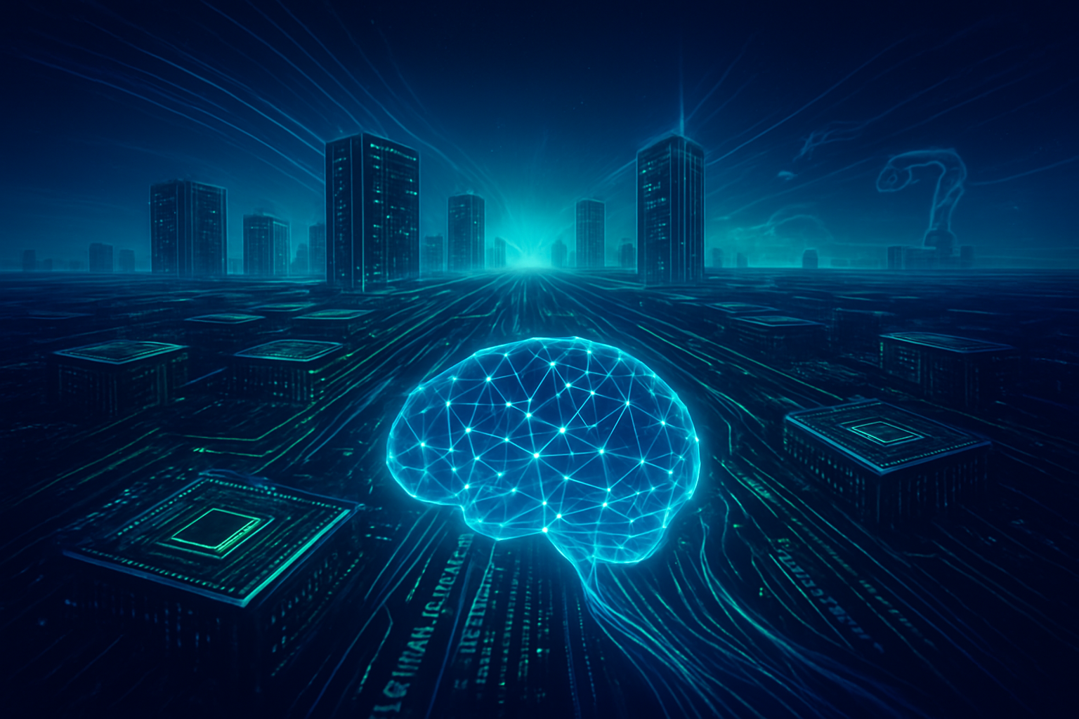
OpenAI's technical strategy for pervasive AI integration is a multi-pronged approach, moving beyond mere conversational agents to embed AI deeply into everyday interactions. At its core, this involves developing highly capable, multimodal, and efficient AI models, coupled with an API-first deployment strategy and a burgeoning interest in dedicated hardware solutions. The company's vision is to create a "suite of superpowers" that fundamentally redefines how humans interact with technology and the world.
Recent advancements underscore this ambition. Models like GPT-4o ("omni" for multimodal) and the newer GPT-5 series represent significant leaps, capable of processing and generating content across text, audio, images, and video. GPT-4o, released in May 2024, can seamlessly act as a real-time translator or math tutor, demonstrating a fluidity in human-computer interaction previously unseen. The even more advanced GPT-5, launched in August 2025, is natively multimodal, trained from scratch on diverse data types simultaneously, leading to superior reasoning capabilities across modalities. This shift from solely scaling models to emphasizing reasoning and efficiency is also evident in approaches like "test-time compute" (seen in models like 'o1' and GPT-5.1), which allows for real-time evaluation of solutions, mimicking human-like problem-solving.
This strategy diverges significantly from previous AI paradigms. While earlier AI focused on specialized tasks or siloed applications, OpenAI aims for deep, ubiquitous integration via robust APIs that allow developers to embed advanced AI into countless applications. Furthermore, their foray into consumer hardware, notably the acquisition of Jony Ive's AI device startup io and commissioning custom AI processors from Broadcom (NASDAQ: AVGO), signals a unique move to integrate AI directly into physical, contextually aware devices. These pocket-sized, screenless gadgets, designed to augment rather than replace existing tech, represent a profound departure from software-centric AI development. The AI research community and industry experts have met these developments with a mixture of awe and caution. While acknowledging the revolutionary capabilities of models like GPT-4o and GPT-5, concerns persist regarding AI safety, ethical implications, potential for misinformation, and job displacement. The intense competition from rivals like Alphabet (NASDAQ: GOOGL) (with Gemini) and Anthropic (with Claude) further highlights the critical balance OpenAI must strike between rapid innovation and responsible development.
Competitive Landscape: Shifting Tides for Tech Giants and Startups
OpenAI's audacious vision for ubiquitous AI integration is fundamentally reshaping the competitive landscape across the technology sector, creating both immense opportunities and significant challenges for established tech giants and agile startups alike. The drive to embed AI seamlessly into every facet of daily life has intensified the race to control the "agentic layer"—the primary interface through which humans will interact with digital services.
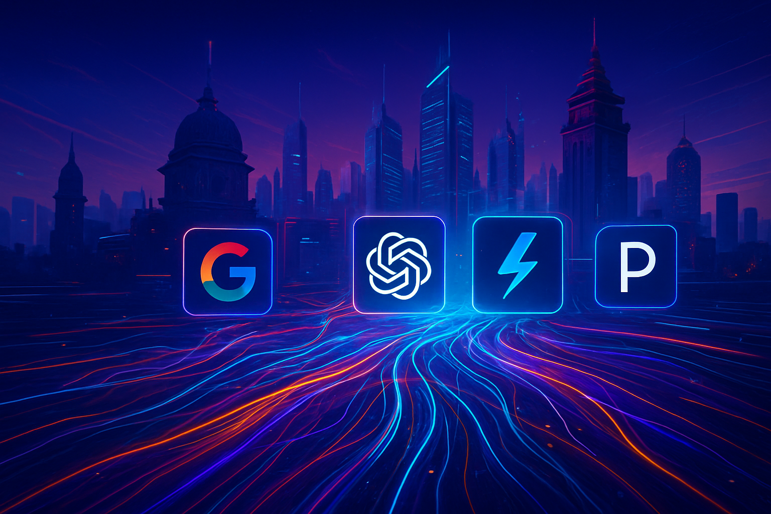
Tech giants are responding with a mix of deep partnerships and aggressive internal development. Microsoft (NASDAQ: MSFT), a major investor in OpenAI, has deeply integrated its models into Azure services and Microsoft 365 through Copilot, aiming to be the premier platform for AI-powered business solutions. Alphabet (NASDAQ: GOOGL), initially caught off guard, has accelerated its own advanced AI, Gemini, leveraging its vast data and Android ecosystem to ensure widespread AI exposure. Apple (NASDAQ: AAPL) has forged a "discreet yet powerful" partnership with OpenAI, integrating ChatGPT into iOS 18 to enhance "Apple Intelligence" across its devices, providing OpenAI access to a massive consumer base. Meanwhile, Oracle (NYSE: ORCL) is integrating OpenAI models into its cloud infrastructure, and Amazon (NASDAQ: AMZN) continues to compete through its Bedrock platform and investments in Anthropic. This fierce competition extends to securing massive compute resources, with OpenAI reportedly making colossal infrastructure commitments to partners like Samsung and SK, and NVIDIA (NASDAQ: NVDA) benefiting as the leading AI chip provider.
For startups, OpenAI's vision presents a double-edged sword. On one hand, accessible APIs and tools lower the barrier to entry, enabling rapid prototyping and reduced development costs. OpenAI actively supports early-stage companies through its $100 million Startup Fund and accelerator programs. On the other hand, the "winner-takes-all" dynamic in foundational models means startups must find niche markets and build highly differentiated, scalable platforms. The commoditization of basic AI execution necessitates a focus on unique value propositions and strong brand positioning to stand out amidst the giants. This era is poised to disrupt numerous existing products and services. AI-powered browsers like OpenAI's Atlas and Perplexity AI's Comet threaten traditional search engines by offering direct answers and multi-step task completion. Productivity suites face disruption as AI agents automate report generation, spreadsheet manipulation, and presentation creation. Customer service, digital marketing, content creation, and even industry-specific software are being transformed by increasingly capable AI, leading to a scramble for strategic advantages rooted in ecosystem control, infrastructure ownership, and the ability to attract top AI talent.
Broader Implications: Reshaping Society and Economy
OpenAI's unwavering vision for ubiquitous AI integration, particularly its relentless pursuit of Artificial General Intelligence (AGI), represents a profound and potentially transformative shift in the technological landscape, aiming to embed AI into nearly every facet of human existence. This ambition extends far beyond specific applications, positioning AI as a foundational utility that will redefine society, the economy, and human capabilities.
This fits squarely within the broader AI landscape's long-term trend towards more generalized and autonomous intelligence. While much of the recent AI revolution has focused on "narrow AI" excelling in specific tasks, OpenAI is at the forefront of the race for AGI—systems capable of human-level cognitive abilities across diverse domains. Many experts predict AGI could arrive within the next five years, signaling an unprecedented acceleration in AI capabilities. OpenAI's strategy, with its comprehensive integration plans and massive infrastructure investments, reflects a belief that AGI will not just be a tool but a foundational layer of future technology, akin to electricity or the internet.
The societal impacts are immense. Ubiquitous AI promises enhanced productivity, an improved quality of life, and greater efficiency across healthcare, education, and climate modeling. AI could automate repetitive jobs, freeing humans for more creative and strategic pursuits. However, this pervasive integration also raises critical concerns regarding privacy, ethical decision-making, and potential societal biases. AI systems trained on vast internet datasets risk perpetuating and amplifying existing stereotypes. The economic impacts are equally profound, with AI projected to add trillions to the global GDP by 2030, driven by increased labor productivity and the creation of new industries. Yet, this transformation carries the risk of widespread job displacement, with estimates suggesting AI could automate 50-70% of existing jobs by 2040, exacerbating wealth inequality and potentially leading to social instability.
In terms of human capabilities, OpenAI envisions AGI as a "force multiplier for human ingenuity and creativity," augmenting intelligence and improving decision-making. However, concerns exist about potential over-reliance on AI diminishing critical thinking and independent decision-making. The ethical considerations are multifaceted, encompassing bias, transparency, accountability, and the "black box" nature of complex AI. Safety and security concerns are also paramount, including the potential for AI misuse (disinformation, deepfakes) and, at the extreme, the loss of human control over highly autonomous systems. OpenAI acknowledges these "catastrophic risks" and has developed frameworks like its "Preparedness Framework" to mitigate them. This pursuit of AGI represents a paradigm shift far exceeding previous AI milestones like early expert systems, the machine learning revolution, or even the deep learning breakthroughs of the last decade. It signifies a potential move from specialized tools to a pervasive, adaptable intelligence that could fundamentally alter human society and the very definition of human capabilities.
The Road Ahead: Anticipating Future Developments
OpenAI's ambitious trajectory towards ubiquitous AI integration promises a future where artificial intelligence is not merely a tool but a foundational, collaborative partner, potentially serving as the operating system for future computing. This journey is characterized by a relentless pursuit of AGI and its seamless embedding into every facet of human activity.
In the near term (1-3 years), significant advancements are expected in autonomous AI agents. OpenAI CEO Sam Altman predicts that by 2025, AI agents will "join the workforce," fundamentally altering company output by performing complex tasks like web browsing, code execution, project management, and research without direct human supervision. OpenAI's "Operator" agent mode within ChatGPT is an early manifestation of this. Enhanced multimodal capabilities will continue to evolve, offering sophisticated video understanding, real-time context-aware audio translation, and advanced spatial reasoning. Future models are also expected to incorporate hybrid reasoning engines and persistent context memory, allowing for long-term learning and personalized interactions. OpenAI is aggressively expanding its enterprise focus, with the Apps SDK enabling ChatGPT to integrate with a wide array of third-party applications, signaling a strategic shift towards broader business adoption. This will be underpinned by massive infrastructure build-outs, including custom hardware partnerships with companies like Broadcom, NVIDIA, and AMD, and next-generation data centers through initiatives like "Project Stargate."
Looking further ahead (5+ years), the attainment of AGI remains OpenAI's foundational mission. CEOs of OpenAI, Alphabet's DeepMind, and Anthropic collectively predict AGI's arrival within the next five years, by 2029 at the latest. The impact of superhuman AI within the next decade is expected to be enormous, potentially exceeding that of the Industrial Revolution. OpenAI anticipates having systems capable of making significant scientific discoveries by 2028 and beyond, accelerating progress in fields like biology, medicine, and climate modeling. The long-term vision includes AI becoming the core "operating system layer" for future computing, providing ubiquitous AI subscriptions and leading to a "widely-distributed abundance" where personalized AI enhances human lives significantly. Generative AI is also expected to shift to billions of edge devices, creating pervasive assistants and creators.
However, the path to ubiquitous AI is fraught with challenges. Ethical and safety concerns, including the potential for misinformation, deepfakes, and the misuse of generative AI, remain paramount. Job displacement and economic transition due to AI automation will necessitate "changes to the social contract." Transparency and trust issues, exacerbated by OpenAI's growing commercial focus, require continuous attention. Technical hurdles for deploying state-of-the-art generative models on edge devices, along with astronomical infrastructure costs and scalability, pose significant financial and engineering challenges. Experts predict a rapid workforce transformation, with AI acting as a "multiplier of effort" but also posing an "existential threat" to companies failing to adapt. While some experts are optimistic, others, though a minority, warn of extreme existential risks if superintelligent AI becomes uncontrollable.
Final Assessment: A New Era of Intelligence
OpenAI's unwavering vision for ubiquitous AI integration, centered on the development of Artificial General Intelligence (AGI), marks a pivotal moment in AI history. The company's mission to ensure AGI benefits all of humanity drives its research, product development, and ethical frameworks, fundamentally reshaping our understanding of AI's role in society.
The key takeaways from OpenAI's strategy are clear: a commitment to human-centric AGI that is safe and aligned with human values, a dedication to democratizing and broadly distributing AI's benefits, and an anticipation of transformative economic and societal impacts. This includes the proliferation of multimodal and agentic AI, capable of seamless interaction across text, audio, and vision, and the emergence of "personal AI agents" that can perform complex tasks autonomously. OpenAI's journey from a non-profit to a "capped-profit" entity, backed by substantial investment from Microsoft (NASDAQ: MSFT), has not only pushed technical boundaries but also ignited widespread public engagement and accelerated global conversations around AI's potential and perils. Its unique charter pledge, even to assist competing AGI projects if they are closer to beneficial AGI, underscores a novel approach to responsible technological advancement.
The long-term impact of this ubiquitous AI vision could be revolutionary, ushering in an era of unprecedented human flourishing. AGI has the potential to solve complex global challenges in health, climate, and education, while redefining work and human purpose by shifting focus from mundane tasks to creative and strategic endeavors. However, this future is fraught with profound challenges. The economic transition, with potential job displacement, will necessitate careful societal planning and a re-evaluation of fundamental socioeconomic contracts. Ethical concerns surrounding bias, misuse, and the concentration of power will demand robust global governance frameworks and continuous vigilance. Maintaining public trust through transparent and ethical practices will be crucial for the long-term success and acceptance of ubiquitous AI. The vision of AI transitioning from a mere tool to a collaborative partner and even autonomous agent suggests a fundamental re-shaping of human-technology interaction, demanding thoughtful adaptation and proactive policy-making.
In the coming weeks and months, the AI landscape will continue to accelerate. All eyes will be on OpenAI for the rumored GPT-5.2 release, potentially around December 9, 2025, which is expected to significantly enhance ChatGPT's performance, speed, and customizability in response to competitive pressures from rivals like Alphabet's (NASDAQ: GOOGL) Gemini 3. Further advancements in multimodal capabilities, enterprise AI solutions, and the development of more sophisticated autonomous AI agents are also anticipated. Any updates regarding OpenAI's reported venture into designing its own AI chips and developments in its safety and ethical frameworks will be critical to watch. The coming period is poised to be one of intense innovation and strategic maneuvering in the AI space, with OpenAI's developments continuing to shape the global trajectory of artificial intelligence.
This content is intended for informational purposes only and represents analysis of current AI developments.
TokenRing AI delivers enterprise-grade solutions for multi-agent AI workflow orchestration, AI-powered development tools, and seamless remote collaboration platforms.
For more information, visit https://www.tokenring.ai/.