Tag: Tech Innovation

  • Beyond Silicon: A New Era of Advanced Materials Ignites Semiconductor Revolution

    Beyond Silicon: A New Era of Advanced Materials Ignites Semiconductor Revolution

    The foundational material of the digital age, silicon, is encountering its inherent physical limits, prompting a pivotal shift in semiconductor manufacturing. While Silicon Carbide (SiC) has rapidly emerged as a dominant force in high-power applications, a new wave of advanced materials is now poised to redefine the very essence of microchip performance and unlock unprecedented capabilities across various industries. This evolution signifies more than an incremental upgrade; it represents a fundamental re-imagining of how electronic devices are built, promising to power the next generation of artificial intelligence, electric vehicles, and beyond.

    This paradigm shift is driven by an escalating demand for chips that can operate at higher frequencies, withstand extreme temperatures, consume less power, and deliver greater efficiency than what traditional silicon can offer. The exploration of materials like Gallium Nitride (GaN), Diamond, Gallium Oxide (Ga₂O₃), and a diverse array of 2D materials promises to overcome current performance bottlenecks, extend the boundaries of Moore's Law, and catalyze a new era of innovation in computing and electronics.

    Unpacking the Technical Revolution: A Deeper Dive into Next-Gen Substrates

    The limitations of silicon, particularly its bandgap and thermal conductivity, have spurred intensive research into alternative materials with superior electronic and thermal properties. Among the most prominent emerging contenders are wide bandgap (WBG) and ultra-wide bandgap (UWBG) semiconductors, alongside novel 2D materials, each offering distinct advantages that silicon struggles to match.

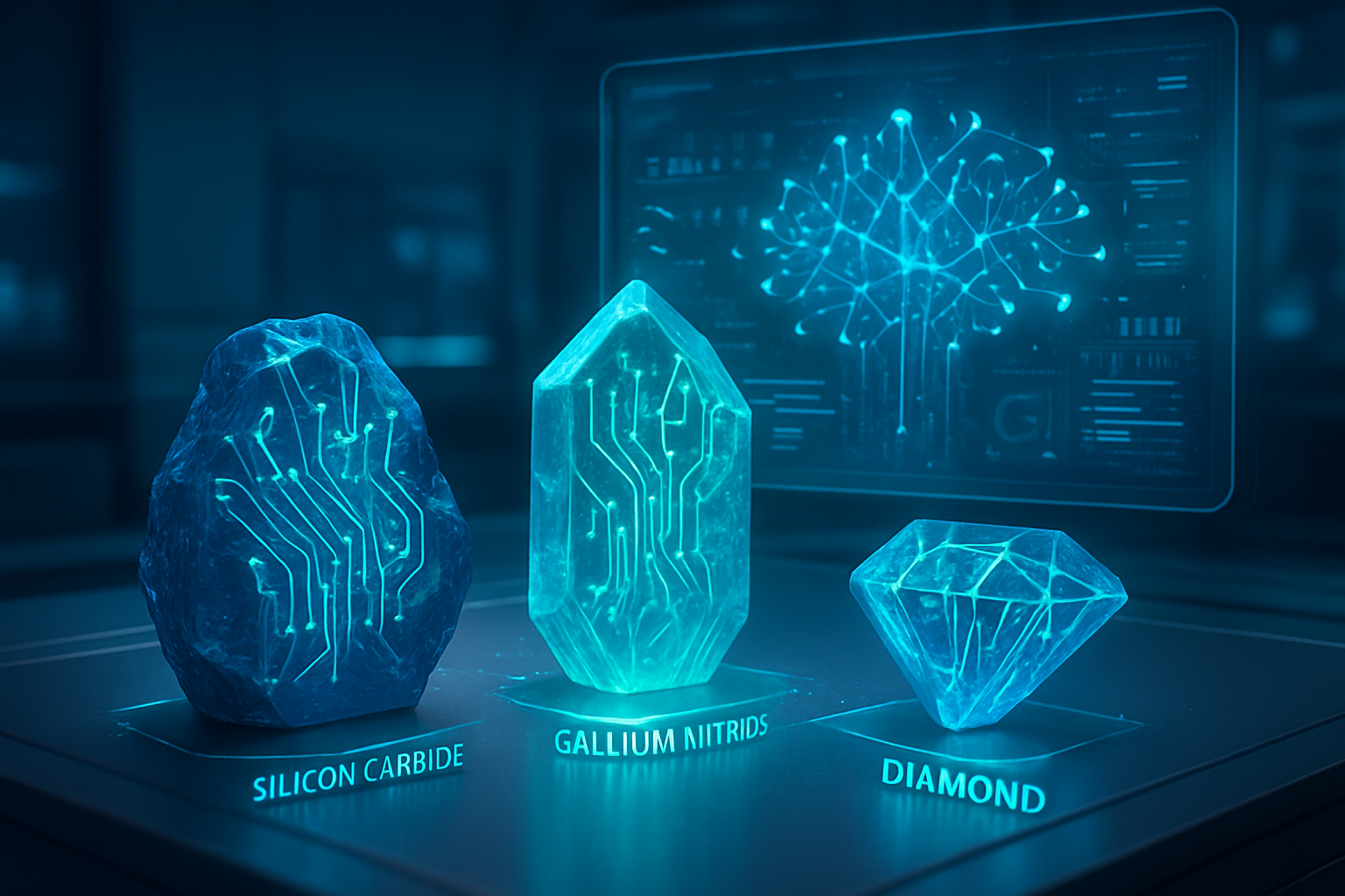
    Gallium Nitride (GaN), already achieving commercial prominence, is a wide bandgap semiconductor (3.4 eV) excelling in high-frequency and high-power applications. Its superior electron mobility and saturation drift velocity allow for faster switching speeds and reduced power loss, making it ideal for power converters, 5G base stations, and radar systems. This directly contrasts with silicon's lower bandgap (1.12 eV), which limits its high-frequency performance and necessitates larger components to manage heat.

    Diamond, an ultra-wide bandgap material (>5.5 eV), is emerging as a "game-changing contender" for extreme environments. Its unparalleled thermal conductivity (approximately 2200 W/m·K compared to silicon's 150 W/m·K) and exceptionally high breakdown electric field (30 times higher than silicon, 3 times higher than SiC) position it for ultra-high-power and high-temperature applications where even SiC might fall short. Researchers are also keenly investigating Gallium Oxide (Ga₂O₃), specifically beta-gallium oxide (β-Ga₂O₃), another UWBG material with significant potential for high-power devices due to its excellent breakdown strength.

    Beyond these, 2D materials like graphene, molybdenum disulfide (MoS₂), and hexagonal boron nitride (h-BN) are being explored for their atomically thin structures and tunable properties. These materials offer avenues for novel transistor designs, flexible electronics, and even quantum computing, allowing for devices with unprecedented miniaturization and functionality. Unlike bulk semiconductors, 2D materials present unique quantum mechanical properties that can be exploited for highly efficient and compact devices. Initial reactions from the AI research community and industry experts highlight the excitement around these materials' potential to enable more efficient AI accelerators, denser memory solutions, and more robust computing platforms, pushing past the thermal and power density constraints currently faced by silicon-based systems. The ability of these materials to operate at higher temperatures and voltages with lower energy losses fundamentally changes the design landscape for future electronics.

    Corporate Crossroads: Reshaping the Semiconductor Industry

    The transition to advanced semiconductor materials beyond silicon and SiC carries profound implications for major tech companies, established chip manufacturers, and agile startups alike. This shift is not merely about adopting new materials but about investing in new fabrication processes, design methodologies, and supply chains, creating both immense opportunities and competitive pressures.

    Companies like Infineon Technologies AG (XTRA: IFX), STMicroelectronics N.V. (NYSE: STM), and ON Semiconductor Corporation (NASDAQ: ON) are already significant players in the SiC and GaN markets, and stand to benefit immensely from the continued expansion and diversification into other WBG and UWBG materials. Their early investments in R&D and manufacturing capacity for these materials give them a strategic advantage in capturing market share in high-growth sectors like electric vehicles, renewable energy, and data centers, all of which demand the superior performance these materials offer.

    The competitive landscape is intensifying as traditional silicon foundries, such as Taiwan Semiconductor Manufacturing Company (TSMC) (NYSE: TSM) and Samsung Electronics Co., Ltd. (KRX: 005930), are also dedicating resources to developing processes for GaN and SiC, and are closely monitoring other emerging materials. Their ability to scale production will be crucial. Startups specializing in novel material synthesis, epitaxy, and device fabrication for diamond or Ga₂O₃, though currently smaller, could become acquisition targets or key partners for larger players seeking to integrate these cutting-edge technologies. For instance, companies like Akhan Semiconductor are pioneering diamond-based devices, demonstrating the disruptive potential of focused innovation.

    This development could disrupt existing product lines for companies heavily reliant on silicon, forcing them to adapt or risk obsolescence in certain high-performance niches. The market positioning will increasingly favor companies that can master the complex manufacturing challenges of these new materials while simultaneously innovating in device design to leverage their unique properties. Strategic alliances, joint ventures, and significant R&D investments will be critical for maintaining competitive edge and navigating the evolving semiconductor landscape.

    Broader Horizons: Impact on AI, IoT, and Beyond

    The shift to advanced semiconductor materials represents a monumental milestone in the broader AI landscape, enabling breakthroughs that were previously unattainable with silicon. The enhanced performance, efficiency, and resilience offered by these materials are perfectly aligned with the escalating demands of modern AI, particularly in areas like high-performance computing (HPC), edge AI, and specialized AI accelerators.

    The ability of GaN and SiC to handle higher power densities and switch faster directly translates to more efficient power delivery systems for AI data centers, reducing energy consumption and operational costs. For AI inferencing at the edge, where power budgets are tight and real-time processing is critical, these materials allow for smaller, more powerful, and more energy-efficient AI chips. Beyond these, materials like diamond and Ga₂O₃, with their extreme thermal stability and breakdown strength, could enable AI systems to operate in harsh industrial environments or even space, expanding the reach of AI applications into new frontiers. The development of 2D materials also holds promise for novel neuromorphic computing architectures, potentially mimicking the brain's efficiency more closely than current digital designs.

    Potential concerns include the higher manufacturing costs and the nascent supply chains for some of these exotic materials, which could initially limit their widespread adoption compared to the mature silicon ecosystem. Scalability remains a challenge for materials like diamond and Ga₂O₃, requiring significant investment in research and infrastructure. However, the benefits in performance, energy efficiency, and operational longevity often outweigh the initial cost, especially in critical applications. This transition can be compared to the move from vacuum tubes to transistors or from germanium to silicon; each step unlocked new capabilities and defined subsequent eras of technological advancement. The current move beyond silicon is poised to have a similar, if not greater, transformative impact.

    The Road Ahead: Anticipating Future Developments and Applications

    The trajectory for advanced semiconductor materials points towards a future characterized by unprecedented performance and diverse applications. In the near term, we can expect continued refinement and cost reduction in GaN and SiC manufacturing, leading to their broader adoption across more consumer electronics, industrial power supplies, and electric vehicle models. The focus will be on improving yield, increasing wafer sizes, and developing more sophisticated device architectures to fully harness their properties.

    Looking further ahead, research and development efforts will intensify on ultra-wide bandgap materials like diamond and Ga₂O₃. Experts predict that as manufacturing techniques mature, these materials will find niches in extremely high-power applications such as next-generation grid infrastructure, high-frequency radar, and potentially even in fusion energy systems. The inherent radiation hardness of diamond, for instance, makes it a prime candidate for electronics operating in hostile environments, including space missions and nuclear facilities.

    For 2D materials, the horizon includes breakthroughs in flexible and transparent electronics, opening doors for wearable AI devices, smart surfaces, and entirely new human-computer interfaces. The integration of these materials into quantum computing architectures also remains a significant area of exploration, potentially enabling more stable and scalable qubits. Challenges that need to be addressed include developing cost-effective and scalable synthesis methods for high-quality single-crystal substrates, improving interface engineering between different materials, and establishing robust testing and reliability standards. Experts predict a future where hybrid semiconductor devices, leveraging the best properties of multiple materials, become commonplace, optimizing performance for specific application requirements.

    Conclusion: A New Dawn for Semiconductors

    The emergence of advanced materials beyond traditional silicon and the rapidly growing Silicon Carbide marks a pivotal moment in semiconductor history. This shift is not merely an evolutionary step but a revolutionary leap, promising to dismantle the performance ceilings imposed by silicon and unlock a new era of innovation. The superior bandgap, thermal conductivity, breakdown strength, and electron mobility of materials like Gallium Nitride, Diamond, Gallium Oxide, and 2D materials are set to redefine chip performance, enabling more powerful, efficient, and resilient electronic devices.

    The key takeaways are clear: the semiconductor industry is diversifying its material foundation to meet the insatiable demands of AI, electric vehicles, 5G/6G, and other cutting-edge technologies. Companies that strategically invest in the research, development, and manufacturing of these advanced materials will gain significant competitive advantages. While challenges in cost, scalability, and manufacturing complexity remain, the potential benefits in performance and energy efficiency are too significant to ignore.

    This development's significance in AI history cannot be overstated. It paves the way for AI systems that are faster, more energy-efficient, capable of operating in extreme conditions, and potentially more intelligent through novel computing architectures. In the coming weeks and months, watch for announcements regarding new material synthesis techniques, expanded manufacturing capacities, and the first wave of commercial products leveraging these truly next-generation semiconductors. The future of computing is no longer solely silicon-based; it is multi-material, high-performance, and incredibly exciting.


    This content is intended for informational purposes only and represents analysis of current AI developments.

    TokenRing AI delivers enterprise-grade solutions for multi-agent AI workflow orchestration, AI-powered development tools, and seamless remote collaboration platforms.
    For more information, visit https://www.tokenring.ai/.

  • The Quantum Leap in Silicon: How Semiconductor Manufacturing is Forging the Future of Hybrid Computing

    The Quantum Leap in Silicon: How Semiconductor Manufacturing is Forging the Future of Hybrid Computing

    The future of computing is rapidly converging at the intersection of quantum mechanics and traditional silicon, promising a revolutionary shift that will redefine the very foundation of digital technology. This isn't about quantum computers entirely replacing classical ones, but rather a profound integration, giving rise to powerful hybrid quantum-classical systems. This immediate significance lies in quantum computing acting as a powerful catalyst, propelling advancements across the entire semiconductor industry and unlocking unprecedented computational capabilities for problems currently intractable for even the most powerful supercomputers.

    The evolution of current chip production to support these nascent quantum technologies is already underway, demanding radical innovations in materials, fabrication, and design. Semiconductor manufacturers are being pushed to develop near-perfect materials, ultra-low noise environments, and specialized cryogenic control electronics capable of operating at extremely low temperatures essential for maintaining delicate quantum states. This drive is accelerating research and development in super-clean interfaces, novel superconductors, and low-defect dielectrics, alongside advancements in sub-nanometer patterning techniques like EUV lithography and 3D integration. The development of "quantum-ready" CMOS and low-power ASICs, alongside new packaging techniques for integrating classical and quantum chips on the same board, underscores a future where traditional chip fabrication lines will adapt to precisely craft and control the building blocks of quantum information, from silicon spin qubits to quantum dots. This symbiotic relationship is not merely an incremental improvement but a foundational paradigm shift, promising faster, more energy-efficient chips and opening doors to breakthroughs in fields from AI-powered chip design to advanced materials discovery.

    Technical Foundations of a Quantum-Silicon Future

    The integration of quantum computing with traditional semiconductor manufacturing represents a pivotal advancement in the quest for scalable and practical quantum systems, moving beyond isolated laboratory setups toward industrial fabrication. Recent breakthroughs center on leveraging complementary metal-oxide-semiconductor (CMOS) technology, the backbone of modern electronics, to fabricate and control qubits. Companies like Equal1 have successfully validated CMOS-compatible silicon spin qubit technology using commercial platforms such as GlobalFoundries' (NASDAQ:GFS) 22FDX, demonstrating the controlled formation of multiple quantum dots with tunable tunnel coupling, a crucial step for building dense qubit arrays. Intel (NASDAQ:INTC) has also made significant strides with its Horse Ridge and Tunnel Falls chips, which integrate quantum control logic directly with classical processors, operating efficiently within cryogenic environments. This includes the development of 48-dot array test chips on 300mm wafers, showcasing the potential for higher qubit densities. Furthermore, IMEC has reported coherent control of hole spin qubits in silicon with single-qubit gate fidelities exceeding 99.9%, incorporating on-chip cryogenic control electronics to enhance performance and scalability. Superconducting qubits are also benefiting from semiconductor integration, with researchers demonstrating their fabrication on high-resistivity silicon substrates, achieving coherence times comparable to those on sapphire substrates (e.g., T1 = 27µs, T2 = 6.6µs for high-resistivity silicon). The development of 3D integration techniques, such as superconducting through-silicon vias (TSVs), further enables high-density superconducting qubit arrays by facilitating complex interconnects between quantum and classical layers.

    This integrated approach marks a significant departure from earlier quantum computing methodologies, which often relied on bulky, external control electronics and highly specialized, non-standard fabrication processes. Previous quantum systems frequently suffered from signal degradation and delays due to long wiring runs between qubits and room-temperature control systems, requiring car-sized hardware for cooling and support. By integrating classical control electronics (cryo-CMOS) directly on the same chip or in the same stack as the qubits, the new approach drastically reduces the physical footprint, minimizes signal loss, improves control speeds, and enhances qubit stability and gate accuracy, even at millikelvin temperatures. This strategic alignment with the established, multi-trillion-dollar semiconductor manufacturing infrastructure promises to unlock unprecedented scalability, enabling the potential for mass production and a significant reduction in the cost and accessibility of quantum technology. The use of existing silicon fabrication techniques helps address the crucial interconnect bottleneck and the complexity of wiring that previously limited the scaling of quantum processors to many thousands of qubits.

    The initial reactions from the AI research community and industry experts to these advancements are a blend of considerable optimism and strategic caution. Many view this integration as ushering in a "transformative phase" and an "AI Supercycle," where AI not only consumes powerful chips but actively participates in their creation and optimization. Experts anticipate the emergence of "Quantum AI," accelerating complex AI algorithms, leading to more sophisticated machine learning models, enhanced data processing, and optimized large-scale logistics across various sectors, including drug discovery, materials science, climate modeling, cybersecurity, and financial risk control. There's a consensus that quantum computers will primarily complement classical systems, acting as powerful accelerators for specific, complex tasks in a hybrid quantum-classical computing paradigm, with some experts predicting quantum advantage for certain problems as early as 2025. The development of technologies like NVIDIA's (NASDAQ:NVDA) NVQLink, which directly couples quantum processors with GPU-accelerated supercomputers, is seen as a critical step in enabling hybrid quantum-classical applications and scaling quantum computing access. However, challenges remain significant, including the extreme fragility of quantum states necessitating ultra-low cryogenic temperatures and specialized packaging, continued high error rates requiring robust error correction protocols, the daunting task of scaling from tens to potentially millions of error-corrected qubits, and the current lack of standardization in hardware and software. There is also a recognized shortage of interdisciplinary talent with expertise spanning quantum physics, computer science, and engineering, which poses a bottleneck for the industry's growth.

    Industry Shifts and Competitive Dynamics

    The integration of quantum computing with traditional semiconductor manufacturing is poised to profoundly impact AI companies, tech giants, and startups, ushering in a new era of computational possibilities and intense competition. This synergy is driven by quantum computing's ability to tackle problems currently intractable for classical machines, particularly in complex optimization, simulation, and advanced AI.

    The benefits will ripple across various types of companies. Traditional Semiconductor Manufacturers such as Intel (NASDAQ:INTC), Taiwan Semiconductor Manufacturing Company (NYSE:TSM) (TSMC), and Samsung (KRX:005930) are well-positioned to benefit by adapting their existing fabrication processes and integrating quantum simulation and optimization into their R&D pipelines. Foundries that embrace quantum-compatible workflows early may gain a strategic edge. AI Chip Developers like NVIDIA (NASDAQ:NVDA), a leader in AI-optimized GPUs, are actively exploring how their hardware can interface with and accelerate quantum workloads, introducing "NVQLink" to integrate conventional AI supercomputers with quantum processors. Tech Giants with Full-Stack Approaches, including IBM (NYSE:IBM), Google (NASDAQ:GOOGL), and Microsoft (NASDAQ:MSFT), are pursuing comprehensive strategies, controlling hardware, software, and cloud access to their quantum systems. IBM offers cloud-based access and is making strides in real-time quantum error correction. Google (Quantum AI) focuses on quantum supremacy and advancing algorithms for AI and machine learning, while Microsoft (Azure Quantum) is developing topological qubits and provides cloud access to various quantum hardware. Amazon (NASDAQ:AMZN) (AWS) offers Amazon Braket, a cloud-based quantum computing platform. Specialized Quantum Hardware and Software Startups, like IonQ (NYSE:IONQ) with trapped-ion technology or Diraq with silicon quantum dots, are crucial innovators, often specializing in niche areas or critical components like cryogenic electronics. Materials Science Companies will also benefit from quantum hardware accelerating the discovery of new materials.

    The integration creates a new competitive landscape. Tech giants like IBM and Google are aiming to establish comprehensive ecosystems by controlling both hardware and software, and providing cloud access to their quantum systems. The most realistic near-term path involves hybrid classical-quantum systems, where quantum accelerators work in conjunction with classical computers, a strategy embraced by companies like NVIDIA with its CUDA-Q and NVQLink platforms. The "quantum advantage" race, where quantum computers demonstrably outperform classical systems, is a key driver of competition, with experts anticipating this milestone within the next 3 to 10 years. The immense cost of quantum R&D and specialized infrastructure could exacerbate the technological divide, and a shortage of quantum computing expertise also hampers widespread adoption. There's a synergistic relationship where AI is increasingly applied to accelerate quantum and semiconductor design, and conversely, quantum computing enhances AI, creating a virtuous cycle benefiting leaders in both fields. Cloud deployment is a dominant market strategy, democratizing access to quantum resources and lowering entry barriers.

    Potential disruptions to existing products or services are significant. The specialized requirements of quantum processors will necessitate rethinking traditional chip designs, manufacturing processes, and materials, potentially leading to a shift in demand towards quantum-enhanced AI hardware. Quantum computing promises to accelerate complex AI algorithms, leading to more sophisticated machine learning models, enhanced data processing, and optimized large-scale logistics, potentially enabling entirely new forms of AI. Quantum machine learning could dramatically speed up how fast AI learns and adapts, cutting training times and reducing energy consumption. Quantum algorithms can revolutionize fields like supply chain routing, financial modeling, drug discovery, and materials science. Furthermore, quantum computing poses a threat to current public-key encryption standards ("Q-Day" around 2030), necessitating a shift to quantum-resistant cryptography, which will disrupt existing cybersecurity products and services but also create a new market for quantum-safe solutions. Quantum technology offers a more sustainable, efficient, and high-performance solution for AI, dramatically lowering costs and increasing scalability while overcoming the energy limitations of today's classical systems.

    In terms of market positioning and strategic advantages, smart semiconductor players are investing modularly, developing quantum-compatible process steps and control electronics. Companies are increasingly embracing hybrid approaches, where quantum computers act as accelerators, integrating with classical supercomputers. Strategic partnerships and collaborations are critical for accelerating R&D and bringing quantum solutions to market. Startups often gain an advantage by specializing in specific qubit architectures, quantum materials, or quantum-classical integration. Tech giants offering cloud-accessible quantum systems gain a significant advantage by democratizing access. Companies are strategically targeting sectors like finance, logistics, pharmaceuticals, and materials science, where quantum computing can offer significant competitive advantages. Early adaptation of foundries to quantum-compatible workflows, materials, and design philosophies stands to gain a strategic edge, with advancements in EUV lithography, atomic-layer processes, and 3D integration driven by quantum chip demands also improving mainstream chip production. Companies like NVIDIA leverage their existing GPU expertise and software platforms (CUDA) to bridge classical and quantum computing, providing a faster path to market for high-end computing applications.

    A New Frontier: Broader Implications and Challenges

    The integration of quantum computing with traditional semiconductor manufacturing represents a pivotal technological convergence with profound wider significance, especially within the evolving Artificial Intelligence (AI) landscape. This synergy promises to unlock unprecedented computational power, redefine manufacturing processes, and overcome current limitations in AI development.

    This integration is poised to revolutionize advanced material discovery and design, enabling the rapid identification and design of advanced materials for more efficient and powerful chips. It will also significantly impact process optimization and manufacturing efficiency by simulating fabrication processes at the quantum level, reducing errors and improving yield. Enhanced chip design capabilities will facilitate the creation of more complex and efficient semiconductor architectures, accelerating the development of advanced chips. Furthermore, quantum computing can offer robust solutions for optimizing intricate global supply chains in the semiconductor industry, improving demand forecasting, inventory management, and logistics planning. As traditional manufacturing techniques approach physical limits, quantum computing offers a promising avenue for enhancing semiconductor design and production processes, potentially evolving or revitalizing Moore's Law into new paradigms.

    This integration is not merely a technological upgrade but a paradigm shift that will profoundly reshape the broader AI landscape. It has the potential to supercharge AI by offering new ways to train models, optimize algorithms, and tackle complex problems beyond the reach of today's classical computers. The insatiable demand for greater computational power and energy efficiency for deep learning and large language models is pushing classical hardware to its breaking point; quantum-semiconductor integration offers a vital pathway to overcome these bottlenecks, providing exponential speed-ups for certain tasks. Quantum machine learning algorithms could process and classify large datasets more efficiently, leading to faster training of AI models and enhanced optimization. Many experts view this integration as a crucial step towards Artificial General Intelligence (AGI), enabling AI models to solve problems currently intractable for classical systems. Conversely, AI itself is being applied to accelerate quantum and semiconductor design, creating a virtuous cycle of innovation.

    The impacts are far-reaching, promising economic growth and an industrial renaissance across various sectors. Quantum-enhanced AI can accelerate scientific breakthroughs, such as drug discovery and new materials development. Quantum computers have the potential for more energy-efficient AI algorithms, crucial for addressing the high power demands of modern AI models. While quantum computers pose a threat to current encryption methods, they are also key to developing quantum-resistant cryptographic algorithms, vital for cybersecurity in a post-quantum world. Leveraging existing semiconductor manufacturing infrastructure is crucial for scaling up quantum processors and making quantum computing more reliable and practical.

    Despite its transformative potential, the integration of quantum computing and semiconductors presents several challenges and concerns. Quantum systems require specialized environments, such as cryogenic cooling, which significantly increases costs and complexity. There is a persistent talent shortage in quantum computing and its integration. Aligning quantum advancements with existing semiconductor processes and ensuring seamless communication between quantum modules and classical IT infrastructure is technically complex. Qubits are fragile and susceptible to noise and decoherence, making error correction a critical hurdle. The immense cost of quantum R&D could exacerbate the technological divide. Ethical considerations surrounding highly advanced AI powered by quantum computing also raise concerns regarding potential biases and the need for robust regulatory frameworks.

    This development is often described as more than just an incremental upgrade; it's considered a fundamental paradigm shift, akin to the transition from Central Processing Units (CPUs) to Graphics Processing Units (GPUs) that fueled the deep learning revolution. Just as GPUs enabled the parallel processing needed for deep learning, quantum computing introduces unprecedented parallelism and data representation capabilities through qubits, moving beyond the traditional limitations of classical physics. Demonstrations like Google's (NASDAQ:GOOGL) Sycamore processor achieving "quantum supremacy" in 2019, solving a complex problem faster than the world's most powerful supercomputers, highlight this transformative potential.

    Charting the Future: Predictions and Pathways

    The integration of quantum computing with traditional semiconductor manufacturing is poised to revolutionize the technology landscape, promising unprecedented computational power and innovative solutions across various industries. This synergy is expected to unfold through near-term advancements and long-term paradigm shifts, addressing complex challenges and opening doors to new applications.

    In the near-term (next 5-10 years), the focus will be on hybrid quantum-classical computing architectures, where quantum processors act as specialized accelerators. This involves classical semiconductor-based interconnects ensuring seamless data exchange. Companies like Intel (NASDAQ:INTC) are actively pursuing silicon spin qubits due to their scalability with advanced lithography and are developing cryogenic control chips like Horse Ridge II, simplifying quantum system operations. By 2025, development teams are expected to increasingly prioritize qubit precision and performance over merely increasing qubit count. Long-term developments envision achieving large-scale quantum processors with thousands or millions of stable qubits, necessitating advanced error correction mechanisms and new semiconductor fabrication facilities capable of handling ultra-pure materials and extreme precision lithography. Innovations in materials science, lithography, and nanofabrication, driven by quantum demands, will spill over into mainstream chip production.

    The integration promises a wide array of applications. In semiconductor manufacturing, quantum algorithms can enhance AI models for improved chip design, enable real-time process monitoring, accelerate material discovery, and optimize fabrication processes. For supply chain management, quantum algorithms can improve demand forecasting, inventory management, and logistics planning. Broader industry impacts include enhanced cybersecurity through quantum cryptography and quantum-resistant algorithms, dramatically reduced AI training times and more sophisticated machine learning models, accelerated drug discovery by simulating molecular interactions, enhanced financial modeling, and more efficient climate modeling.

    Despite the immense potential, several significant challenges must be overcome. These include the high infrastructure requirements for cryogenic cooling, a persistent talent shortage, complex compatibility issues between quantum and classical components, and the critical need for maintaining quantum coherence and robust error correction. High research and development costs, low manufacturing yields, and the existence of competing qubit architectures also pose hurdles. Managing thermal dissipation, mitigating gate-oxide defects, and developing efficient interfaces and control electronics are crucial. Furthermore, quantum computing introduces new types of data that require different storage and management approaches.

    Experts foresee a transformative future. Many anticipate reaching "quantum advantage"—where quantum computers demonstrably outperform classical machines for certain useful tasks—within the next 3 to 5 years, with some extending this to 5 to 10 years. There's a growing awareness of "Q-Day," estimated around 2030, when quantum computers could break current public-key encryption standards, accelerating investment in quantum-resistant cryptography. By 2025, a greater emphasis will be placed on qubit precision and performance rather than just the raw qubit count. The quantum ecosystem will mature with increased collaboration, driving faster commercialization and adoption, with "quantum platforms" offering seamless integration of classical, AI, and quantum resources. Quantum design tools are expected to become standard in advanced semiconductor R&D within the next decade. Quantum computing is not expected to replace traditional semiconductors entirely but will act as a powerful catalyst for progress, positioning early adaptors at the forefront of the next computing revolution. The global quantum hardware market, specifically the quantum chip market, is projected to reach USD 7.04 billion by 2032.

    A New Era of Computational Power Dawns

    The integration of quantum computing with traditional semiconductor manufacturing marks a pivotal moment in the evolution of technology, promising to redefine the very limits of computation and innovation. This symbiotic relationship is set to usher in an era of hybrid quantum-classical systems, where the exponential power of quantum mechanics augments the established reliability of silicon-based electronics. Key takeaways from this impending revolution include the critical advancements in CMOS-compatible qubit fabrication, the development of specialized cryogenic control electronics, and the strategic shift towards hybrid architectures that leverage the strengths of both classical and quantum paradigms.

    This development's significance in AI history cannot be overstated. It represents a potential leap comparable to, if not exceeding, the transition from CPUs to GPUs that fueled the deep learning revolution. By enabling the processing of previously intractable problems, this integration offers the computational horsepower necessary to unlock more sophisticated AI models, accelerate scientific discovery, and optimize complex systems across nearly every industry. While challenges such as qubit fragility, error correction, and the immense cost of R&D remain, the concerted efforts of tech giants, specialized startups, and academic institutions are steadily pushing the boundaries of what's possible.

    Looking ahead, the coming weeks and months will likely see continued breakthroughs in qubit stability and coherence, further integration of control electronics onto the quantum chip, and the maturation of software platforms designed to bridge the classical-quantum divide. The race for "quantum advantage" will intensify, potentially leading to demonstrable real-world applications within the next few years. As the semiconductor industry adapts to meet the exacting demands of quantum technologies, we can expect a cascade of innovations that will not only advance quantum computing but also push the boundaries of classical chip design and manufacturing. The long-term impact promises a future where AI, supercharged by quantum capabilities, tackles humanity's most complex problems, from climate change to personalized medicine, fundamentally transforming our world.


    This content is intended for informational purposes only and represents analysis of current AI developments.

    TokenRing AI delivers enterprise-grade solutions for multi-agent AI workflow orchestration, AI-powered development tools, and seamless remote collaboration platforms.
    For more information, visit https://www.tokenring.ai/.

  • The Silicon Frontier: Charting the Course for Next-Gen AI Hardware

    The Silicon Frontier: Charting the Course for Next-Gen AI Hardware

    The relentless march of artificial intelligence is pushing the boundaries of what's possible, but its ambitious future is increasingly contingent on a fundamental transformation in the very silicon that powers it. As AI models grow exponentially in complexity, demanding unprecedented computational power and energy efficiency, the industry stands at the precipice of a hardware revolution. The current paradigm, largely reliant on adapted general-purpose processors, is showing its limitations, paving the way for a new era of specialized semiconductors and architectural innovations designed from the ground up to unlock the full potential of next-generation AI.

    The immediate significance of this shift cannot be overstated. From the development of advanced multimodal AI capable of understanding and generating human-like content across various mediums, to agentic AI systems that make autonomous decisions, and physical AI driving robotics and autonomous vehicles, each leap forward hinges on foundational hardware advancements. The race is on to develop chips that are not just faster, but fundamentally more efficient, scalable, and capable of handling the diverse, complex, and real-time demands of an intelligent future.

    Beyond the Memory Wall: Architectural Innovations and Specialized Silicon

    The technical underpinnings of this hardware revolution are multifaceted, targeting the core inefficiencies and bottlenecks of current computing architectures. At the heart of the challenge lies the "memory wall" – a bottleneck inherent in the traditional Von Neumann architecture, where the constant movement of data between separate processing units and memory consumes significant energy and time. To overcome this, innovations are emerging on several fronts.

    One of the most promising architectural shifts is in-memory computing, or processing-in-memory (PIM), where computations are performed directly within or very close to the memory units. This drastically reduces the energy and latency associated with data transfer, a critical advantage for memory-intensive AI workloads like large language models (LLMs). Simultaneously, neuromorphic computing, inspired by the human brain's structure, seeks to mimic biological neural networks for highly energy-efficient and adaptive learning. These chips, like Intel's (NASDAQ: INTC) Loihi or IBM's (NYSE: IBM) NorthPole, promise a future of AI that learns and adapts with significantly less power.

    In terms of semiconductor technologies, the industry is exploring beyond traditional silicon. Photonic computing, which uses light instead of electrons for computation, offers the potential for orders of magnitude improvements in speed and energy efficiency for specific AI tasks like image recognition. Companies are developing light-powered chips that could achieve up to 100 times greater efficiency and faster processing. Furthermore, wide-bandgap (WBG) semiconductors like Gallium Nitride (GaN) and Silicon Carbide (SiC) are gaining traction for their superior power density and efficiency, making them ideal for high-power AI data centers and crucial for reducing the massive energy footprint of AI.

    These advancements represent a significant departure from previous approaches, which primarily focused on scaling up general-purpose GPUs. While GPUs, particularly those from Nvidia (NASDAQ: NVDA), have been the workhorses of the AI revolution due to their parallel processing capabilities, their general-purpose nature means they are not always optimally efficient for every AI task. The new wave of hardware is characterized by heterogeneous integration and chiplet architectures, where specialized components (CPUs, GPUs, NPUs, ASICs) are integrated within a single package, each optimized for specific parts of an AI workload. This modular approach, along with advanced packaging and 3D stacking, allows for greater flexibility, higher performance, and improved yields compared to monolithic chip designs. Initial reactions from the AI research community and industry experts are largely enthusiastic, recognizing these innovations as essential for sustaining the pace of AI progress and making it more sustainable. The consensus is that while general-purpose accelerators will remain important, specialized and integrated solutions are the key to unlocking the next generation of AI capabilities.

    The New Arms Race: Reshaping the AI Industry Landscape

    The emergence of these advanced AI hardware technologies is not merely an engineering feat; it's a strategic imperative that is profoundly reshaping the competitive landscape for AI companies, tech giants, and burgeoning startups. The ability to design, manufacture, or access cutting-edge AI silicon is becoming a primary differentiator, driving a new "arms race" in the technology sector.

    Tech giants with deep pockets and extensive R&D capabilities are at the forefront of this transformation. Companies like Nvidia (NASDAQ: NVDA) continue to dominate with their powerful GPUs and comprehensive software ecosystems, constantly innovating with new architectures like Blackwell. However, they face increasing competition from other behemoths. Google (NASDAQ: GOOGL) leverages its custom Tensor Processing Units (TPUs) to power its AI initiatives and cloud services, while Amazon (NASDAQ: AMZN) with AWS, and Microsoft (NASDAQ: MSFT) with Azure, are heavily investing in their own custom AI chips (like Amazon's Inferentia and Trainium, and Microsoft's Azure Maia 100) to optimize their cloud AI offerings. This vertical integration allows them to offer unparalleled performance and efficiency, attracting enterprises and reinforcing their market leadership. Intel (NASDAQ: INTC) is also making significant strides with its Gaudi AI accelerators and re-entering the foundry business to secure its position in this evolving market.

    The competitive implications are stark. The intensified competition is driving rapid innovation, but also leading to a diversification of hardware options, reducing dependency on a single supplier. "Hardware is strategic again" is a common refrain, as control over computing power becomes a critical component of national security and strategic influence. For startups, while the barrier to entry can be high due to the immense cost of developing cutting-edge chips, open-source hardware initiatives like RISC-V are democratizing access to customizable designs. This allows nimble startups to carve out niche markets, focusing on specialized AI hardware for edge computing or specific generative AI models. Companies like Groq, known for its ultra-fast inference chips, demonstrate the potential for startups to disrupt established players by focusing on specific, high-demand AI workloads.

    This shift also brings potential disruptions to existing products and services. General-purpose CPUs, while foundational, are becoming less suitable for sophisticated AI tasks, losing ground to specialized ASICs and GPUs. The rise of "AI PCs" equipped with Neural Processing Units (NPUs) signifies a move towards embedding AI capabilities directly into end-user devices, reducing reliance on cloud computing for some tasks, enhancing data privacy, and potentially "future-proofing" technology infrastructure. This evolution could shift some AI workloads from the cloud to the edge, creating new form factors and interfaces that prioritize AI-centric functionality. Ultimately, companies that can effectively integrate these new hardware paradigms into their products and services will gain significant strategic advantages, offering enhanced performance, greater energy efficiency, and the ability to enable real-time, sophisticated AI applications across diverse sectors.

    A New Era of Intelligence: Broader Implications and Looming Challenges

    The advancements in AI hardware and architectural innovations are not isolated technical achievements; they are the foundational bedrock upon which the next era of artificial intelligence will be built, fitting seamlessly into and accelerating broader AI trends. This symbiotic relationship between hardware and software is fueling the exponential growth of capabilities in areas like large language models (LLMs) and generative AI, which demand unprecedented computational power for both training and inference. The ability to process vast datasets and complex algorithms more efficiently is enabling AI to move beyond its current capabilities, facilitating advancements that promise more human-like reasoning and robust decision-making.

    A significant trend being driven by this hardware revolution is the proliferation of Edge AI. Specialized, low-power hardware is enabling AI to move from centralized cloud data centers to local devices – smartphones, autonomous vehicles, IoT sensors, and robotics. This shift allows for real-time processing, reduced latency, enhanced data privacy, and the deployment of AI in environments where constant cloud connectivity is impractical. The emergence of "AI PCs" equipped with Neural Processing Units (NPUs) is a testament to this trend, bringing sophisticated AI capabilities directly to the user's desktop, assisting with tasks and boosting productivity locally. These developments are not just about raw power; they are about making AI more ubiquitous, responsive, and integrated into our daily lives.

    However, this transformative progress is not without its significant challenges and concerns. Perhaps the most pressing is the energy consumption of AI. Training and running complex AI models, especially LLMs, consume enormous amounts of electricity. Projections suggest that data centers, heavily driven by AI workloads, could account for a substantial portion of global electricity use by 2030-2035, putting immense strain on power grids and contributing significantly to greenhouse gas emissions. The demand for water for cooling these vast data centers also presents an environmental concern. Furthermore, the cost of high-performance AI hardware remains prohibitive for many, creating an accessibility gap that concentrates cutting-edge AI development among a few large organizations. The rapid obsolescence of AI chips also contributes to a growing e-waste problem, adding another layer of environmental impact.

    Comparing this era to previous AI milestones highlights the unique nature of the current moment. The early AI era, relying on general-purpose CPUs, was largely constrained by computational limits. The GPU revolution, spearheaded by Nvidia (NASDAQ: NVDA) in the 2010s, unleashed parallel processing, leading to breakthroughs in deep learning. However, the current era, characterized by purpose-built AI chips (like Google's (NASDAQ: GOOGL) TPUs, ASICs, and NPUs) and radical architectural innovations like in-memory computing and neuromorphic designs, represents a leap in performance and efficiency that was previously unimaginable. Unlike past "AI winters," where expectations outpaced technological capabilities, today's hardware advancements provide the robust foundation for sustained software innovation, ensuring that the current surge in AI development is not just a fleeting trend but a fundamental shift towards a truly intelligent future.

    The Road Ahead: Near-Term Innovations and Distant Horizons

    The trajectory of AI hardware development points to a future of relentless innovation, driven by the insatiable computational demands of advanced AI models and the critical need for greater efficiency. In the near term, spanning late 2025 through 2027, the industry will witness an intensifying focus on custom AI silicon. Application-Specific Integrated Circuits (ASICs), Neural Processing Units (NPUs), and Tensor Processing Units (TPUs) will become even more prevalent, meticulously engineered for specific AI tasks to deliver superior speed, lower latency, and reduced energy consumption. While Nvidia (NASDAQ: NVDA) is expected to continue its dominance with new GPU architectures like Blackwell and the upcoming Rubin models, it faces growing competition. Qualcomm is launching new AI accelerator chips for data centers (AI200 in 2026, AI250 in 2027), optimized for inference, and AMD (NASDAQ: AMD) is strengthening its position with the MI350 series. Hyperscale cloud providers like Google (NASDAQ: GOOGL), Amazon (NASDAQ: AMZN), and Microsoft (NASDAQ: MSFT) are also deploying their own specialized silicon to reduce external reliance and offer optimized cloud AI services. Furthermore, advancements in High-Bandwidth Memory (HBM4) and interconnects like Compute Express Link (CXL) are crucial for overcoming memory bottlenecks and improving data transfer efficiency.

    Looking further ahead, beyond 2027, the landscape promises even more radical transformations. Neuromorphic computing, which aims to mimic the human brain's structure and function with highly efficient artificial synapses and neurons, is poised to deliver unprecedented energy efficiency and performance for tasks like pattern recognition. Companies like Intel (NASDAQ: INTC) with Loihi 2 and IBM (NYSE: IBM) with TrueNorth are at the forefront of this field, striving for AI systems that consume minimal energy while achieving powerful, brain-like intelligence. Even more distantly, Quantum AI hardware looms as a potentially revolutionary force. While still in early stages, the integration of quantum computing with AI could redefine computing by solving complex problems faster and more accurately than classical computers. Hybrid quantum-classical computing, where AI workloads utilize both quantum and classical machines, is an anticipated near-term step. The long-term vision also includes reconfigurable hardware that can dynamically adapt its architecture during AI execution, whether at the edge or in the cloud, to meet evolving algorithmic demands.

    These advancements will unlock a vast array of new applications. Real-time AI will become ubiquitous in autonomous vehicles, industrial robots, and critical decision-making systems. Edge AI will expand significantly, embedding sophisticated intelligence into smart homes, wearables, and IoT devices with enhanced privacy and reduced cloud dependence. The rise of Agentic AI, focused on autonomous decision-making, will enable companies to "employ" and train AI workers to integrate into hybrid human-AI teams, demanding low-power hardware optimized for natural language processing and perception. Physical AI will drive progress in robotics and autonomous systems, emphasizing embodiment and interaction with the physical world. In healthcare, agentic AI will lead to more sophisticated diagnostics and personalized treatments. However, significant challenges remain, including the high development costs of custom chips, the pervasive issue of energy consumption (with data centers projected to consume 20% of global electricity by 2025), hardware fragmentation, supply chain vulnerabilities, and the sheer architectural complexity of these new systems. Experts predict continued market expansion for AI chips, a diversification beyond GPU dominance, and a necessary rebalancing of investment towards AI infrastructure to truly unlock the technology's massive potential.

    The Foundation of Future Intelligence: A Comprehensive Wrap-Up

    The journey into the future of AI hardware reveals a landscape of profound transformation, where specialized silicon and innovative architectures are not just desirable but essential for the continued evolution of artificial intelligence. The key takeaway is clear: the era of relying solely on adapted general-purpose processors for advanced AI is rapidly drawing to a close. We are witnessing a fundamental shift towards purpose-built, highly efficient, and diverse computing solutions designed to meet the escalating demands of complex AI models, from massive LLMs to sophisticated agentic systems.

    This moment holds immense significance in AI history, akin to the GPU revolution that ignited the deep learning boom. However, it surpasses previous milestones by tackling the core inefficiencies of traditional computing head-on, particularly the "memory wall" and the unsustainable energy consumption of current AI. The long-term impact will be a world where AI is not only more powerful and intelligent but also more ubiquitous, responsive, and seamlessly integrated into every facet of society and industry. This includes the potential for AI to tackle global-scale challenges, from climate change to personalized medicine, driving an estimated $11.2 trillion market for AI models focused on business inference.

    In the coming weeks and months, several critical developments bear watching. Anticipate a flurry of new chip announcements and benchmarks from major players like Nvidia (NASDAQ: NVDA), AMD (NASDAQ: AMD), Intel (NASDAQ: INTC), Google (NASDAQ: GOOGL), Amazon (NASDAQ: AMZN), and Microsoft (NASDAQ: MSFT), particularly their performance on generative AI tasks. Keep an eye on strategic investments and partnerships aimed at securing critical compute power and expanding AI infrastructure. Monitor the progress in alternative architectures like neuromorphic and quantum computing, as any significant breakthroughs could signal major paradigm shifts. Geopolitical developments concerning export controls and domestic chip production will continue to shape the global supply chain. Finally, observe the increasing proliferation and capabilities of "AI PCs" and other edge devices, which will demonstrate the decentralization of AI processing, and watch for sustainability initiatives addressing the environmental footprint of AI. The future of AI is being forged in silicon, and its evolution will define the capabilities of intelligence itself.


    This content is intended for informational purposes only and represents analysis of current AI developments.

    TokenRing AI delivers enterprise-grade solutions for multi-agent AI workflow orchestration, AI-powered development tools, and seamless remote collaboration platforms.
    For more information, visit https://www.tokenring.ai/.
  • Brain-Inspired Breakthroughs: Neuromorphic Computing Poised to Reshape AI’s Future

    Brain-Inspired Breakthroughs: Neuromorphic Computing Poised to Reshape AI’s Future

    In a significant leap towards more efficient and biologically plausible artificial intelligence, neuromorphic computing is rapidly advancing, moving from the realm of academic research into practical, transformative applications. This revolutionary field, which draws direct inspiration from the human brain's architecture and operational mechanisms, promises to overcome the inherent limitations of traditional computing, particularly the "von Neumann bottleneck." As of October 27, 2025, developments in brain-inspired chips are accelerating, heralding a new era of AI that is not only more powerful but also dramatically more sustainable and adaptable.

    The immediate significance of neuromorphic computing lies in its ability to address critical challenges facing modern AI, such as escalating energy consumption and the need for real-time, on-device intelligence. By integrating processing and memory and adopting event-driven, spiking neural networks (SNNs), these systems offer unparalleled energy efficiency and the capacity for continuous, adaptive learning. This makes them ideally suited for a burgeoning array of applications, from always-on edge AI devices and autonomous systems to advanced healthcare diagnostics and robust cybersecurity solutions, paving the way for truly intelligent systems that can operate with human-like efficiency.

    The Architecture of Tomorrow: Technical Prowess and Community Acclaim

    Neuromorphic architecture fundamentally redefines how computation is performed, moving away from the sequential, data-shuttling model of traditional computers. At its core, it employs artificial neurons and synapses that communicate via discrete "spikes" or electrical pulses, mirroring biological neurons. This event-driven processing means computations are only triggered when relevant spikes are detected, leading to sparse, highly energy-efficient operations. Crucially, neuromorphic chips integrate processing and memory within the same unit, eliminating the "memory wall" that plagues conventional systems and drastically reducing latency and power consumption. Hardware implementations leverage diverse technologies, including memristors for synaptic plasticity, ultra-thin materials for efficient switches, and emerging materials like bacterial protein nanowires for novel neuron designs.

    Several significant advancements underscore this technical shift. IBM Corporation (NYSE: IBM), with its TrueNorth and NorthPole chips, has demonstrated large-scale neurosynaptic systems. Intel Corporation (NASDAQ: INTC) has made strides with its Loihi and Loihi 2 research chips, designed for asynchronous spiking neural networks and achieving milliwatt-level power consumption for specific tasks. More recently, BrainChip Holdings Ltd. (ASX: BRN) launched its Akida processor, an entirely digital, event-oriented AI processor, followed by the Akida Pulsar neuromorphic microcontroller, offering 500 times lower energy consumption and 100 times latency reduction compared to conventional AI cores for sensor edge applications. The Chinese Academy of Sciences' "Speck" chip and its accompanying SpikingBrain-1.0 model, unveiled in 2025, consume a negligible 0.42 milliwatts when idle and require only about 2% of the pre-training data of conventional models. Meanwhile, KAIST introduced a "Frequency Switching Neuristor" in September 2025, mimicking intrinsic plasticity and showing a 27.7% energy reduction in simulations, and UMass Amherst researchers created artificial neurons powered by bacterial protein nanowires in October 2025, showcasing biologically inspired energy efficiency.

    The distinction from previous AI hardware, particularly GPUs, is stark. While GPUs excel at dense, synchronous matrix computations, neuromorphic chips are purpose-built for sparse, asynchronous, event-driven processing. This specialization translates into orders of magnitude greater energy efficiency for certain AI workloads. For instance, while high-end GPUs can consume hundreds to thousands of watts, neuromorphic solutions often operate in the milliwatt to low-watt range, aiming to emulate the human brain's approximate 20-watt power consumption. The AI research community and industry experts have largely welcomed these developments, recognizing neuromorphic computing as a vital solution to the escalating energy footprint of AI and a "paradigm shift" that could revolutionize AI by enabling brain-inspired information processing. Despite the optimism, challenges remain in standardization, developing robust software ecosystems, and avoiding the "buzzword" trap, ensuring adherence to true biological inspiration.

    Reshaping the AI Industry: A New Competitive Landscape

    The advent of neuromorphic computing is poised to significantly realign the competitive landscape for AI companies, tech giants, and startups. Companies with foundational research and commercial products in this space stand to gain substantial strategic advantages.

    Intel Corporation (NASDAQ: INTC) and IBM Corporation (NYSE: IBM) are well-positioned, having invested heavily in neuromorphic research for years. Their continued advancements, such as Intel's Hala Point system (simulating 1.15 billion neurons) and IBM's NorthPole, underscore their commitment. Samsung Electronics Co. Ltd. (KRX: 005930) and Qualcomm Incorporated (NASDAQ: QCOM) are also key players, leveraging neuromorphic principles to enhance memory and processing efficiency for their vast ecosystems of smart devices and IoT applications. BrainChip Holdings Ltd. (ASX: BRN) has emerged as a leader with its Akida processor, specifically designed for low-power, real-time AI processing across diverse industries. While NVIDIA Corporation (NASDAQ: NVDA) currently dominates the AI hardware market with GPUs, the rise of neuromorphic chips could disrupt its stronghold in specific inference workloads, particularly those requiring ultra-low power and real-time processing at the edge. However, NVIDIA is also investing in advanced AI chip design, ensuring its continued relevance.

    A vibrant ecosystem of startups is also driving innovation, often focusing on niche, ultra-efficient solutions. Companies like SynSense (formerly aiCTX) are developing high-speed, ultra-low-latency neuromorphic chips for applications in bio-signal analysis and smart cameras. Innatera (Netherlands) recently unveiled its SNP (Spiking Neural Processor) at CES 2025, boasting sub-milliwatt power dissipation for ambient intelligence. Other notable players include Mythic AI, Polyn Technology, Aspirare Semi, and Grayscale AI, each carving out strategic advantages in areas like edge AI, autonomous robotics, and ultra-low-power sensing. These companies are capitalizing on the performance-per-watt advantage offered by neuromorphic architectures, which is becoming a critical metric in the competitive AI hardware market.

    This shift implies potential disruption to existing products and services, particularly in areas constrained by power and real-time processing. Edge AI and IoT devices, autonomous vehicles, and wearable technology are prime candidates for transformation, as neuromorphic chips enable more sophisticated AI directly on the device, reducing reliance on cloud infrastructure. This also has profound implications for sustainability, as neuromorphic computing could significantly reduce AI's global energy consumption. Companies that master the unique training algorithms and software ecosystems required for neuromorphic systems will gain a competitive edge, fostering a predicted shift towards a co-design approach where hardware and software are developed in tandem. The neuromorphic computing market is projected for significant growth, with estimates suggesting it could reach $4.1 billion by 2029, powering 30% of edge AI devices by 2030, highlighting a rapidly evolving landscape where innovation will be paramount.

    A New Horizon for AI: Wider Significance and Ethical Imperatives

    Neuromorphic computing represents more than just an incremental improvement in AI hardware; it signifies a fundamental re-evaluation of how artificial intelligence is conceived and implemented. By mirroring the brain's integrated processing and memory, it directly addresses the energy and latency bottlenecks that limit traditional AI, aligning perfectly with the growing trends of edge AI, energy-efficient computing, and real-time adaptive learning. This paradigm shift holds the promise of enabling AI that is not only more powerful but also inherently more sustainable and responsive to dynamic environments.

    The impacts are far-reaching. In autonomous systems and robotics, neuromorphic chips can provide the real-time, low-latency decision-making crucial for safe and efficient operation. In healthcare, they offer the potential for faster, more accurate diagnostics and advanced brain-machine interfaces. For the Internet of Things (IoT), these chips enable sophisticated AI capabilities on low-power, battery-operated devices, expanding the reach of intelligent systems. Environmentally, the most compelling impact is the potential for significant reductions in AI's massive energy footprint, contributing to global sustainability goals.

    However, this transformative potential also comes with significant concerns. Technical challenges persist, including the need for more robust software algorithms, standardization, and cost-effective fabrication processes. Ethical dilemmas loom, similar to other advanced AI, but intensified by neuromorphic computing's brain-like nature: questions of artificial consciousness, autonomy and control of highly adaptive systems, algorithmic bias, and privacy implications arising from pervasive, real-time data processing. The complexity of these systems could make transparency and explainability difficult, potentially eroding public trust.

    Comparing neuromorphic computing to previous AI milestones reveals its unique position. While breakthroughs like symbolic AI, expert systems, and the deep learning revolution focused on increasing computational power or algorithmic efficiency, neuromorphic computing tackles a more fundamental hardware limitation: energy consumption and the von Neumann bottleneck. It champions biologically inspired efficiency over brute-force computation, offering a path to AI that is not only intelligent but also inherently efficient, mirroring the elegance of the human brain. While still in its early stages compared to established deep learning, experts view it as a critical development, potentially as significant as the invention of the transistor or the backpropagation algorithm, offering a pathway to overcome some of deep learning's current limitations, such as its data hunger and high energy demands.

    The Road Ahead: Charting Neuromorphic AI's Future

    The journey of neuromorphic computing is accelerating, with clear near-term and long-term trajectories. In the next 5-10 years, hybrid systems that integrate neuromorphic chips as specialized accelerators alongside traditional CPUs and GPUs will become increasingly common. Hardware advancements will continue to focus on novel materials like memristors and spintronic devices, leading to denser, faster, and more efficient chips. Intel's Hala Point, a neuromorphic system with 1,152 Loihi 2 processors, is a prime example of this scalable, energy-efficient AI computing. Furthermore, BrainChip Holdings Ltd. (ASX: BRN) is set to expand access to its Akida 2 technology with the launch of Akida Cloud in August 2025, facilitating prototyping and inference. The development of more robust software and algorithmic ecosystems for spike-based learning will also be a critical near-term focus.

    Looking beyond a decade, neuromorphic computing is poised to become a more mainstream computing paradigm, potentially leading to truly brain-like computers capable of unprecedented parallel processing and adaptive learning with minimal power consumption. This long-term vision includes the exploration of 3D neuromorphic chips and even the integration of quantum computing principles to create "quantum neuromorphic" systems, pushing the boundaries of computational capability. Experts predict that biological-scale networks are not only possible but inevitable, with the primary challenge shifting from hardware to creating the advanced algorithms needed to fully harness these systems.

    The potential applications on the horizon are vast and transformative. Edge computing and IoT devices will be revolutionized by neuromorphic chips, enabling smart sensors to process complex data locally, reducing bandwidth and power consumption. Autonomous vehicles and robotics will benefit from real-time, low-latency decision-making with minimal power draw, crucial for safety and efficiency. In healthcare, advanced diagnostic tools, medical imaging, and even brain-computer interfaces could see significant enhancements. The overarching challenge remains the complexity of the domain, requiring deep interdisciplinary collaboration across biology, computer science, and materials engineering. Cost, scalability, and the absence of standardized programming frameworks and benchmarks are also significant hurdles that must be overcome for widespread adoption. Nevertheless, experts anticipate a gradual but steady shift towards neuromorphic integration, with the market for neuromorphic hardware projected to expand at a CAGR of 20.1% from 2025 to 2035, becoming a key driver for sustainability in computing.

    A Transformative Era for AI: The Dawn of Brain-Inspired Intelligence

    Neuromorphic computing stands at a pivotal moment, representing a profound shift in the foundational approach to artificial intelligence. The key takeaways from current developments are clear: these brain-inspired chips offer unparalleled energy efficiency, real-time processing capabilities, and adaptive learning, directly addressing the growing energy demands and latency issues of traditional AI. By integrating processing and memory and utilizing event-driven spiking neural networks, neuromorphic systems are not merely faster or more powerful; they are fundamentally more sustainable and biologically plausible.

    This development marks a significant milestone in AI history, potentially rivaling the impact of earlier breakthroughs by offering a path towards AI that is not only intelligent but also inherently efficient, mirroring the elegance of the human brain. While still facing challenges in software development, standardization, and cost, the rapid advancements from companies like Intel Corporation (NASDAQ: INTC), IBM Corporation (NYSE: IBM), and BrainChip Holdings Ltd. (ASX: BRN), alongside a burgeoning ecosystem of innovative startups, indicate a technology on the cusp of widespread adoption. Its potential to revolutionize edge AI, autonomous systems, healthcare, and to significantly mitigate AI's environmental footprint underscores its long-term impact.

    In the coming weeks and months, the tech world should watch for continued breakthroughs in neuromorphic hardware, particularly in the integration of novel materials and 3D architectures. Equally important will be the development of more accessible software frameworks and programming models that can unlock the full potential of these unique processors. As research progresses and commercial applications mature, neuromorphic computing is poised to usher in an era of truly intelligent, adaptive, and sustainable AI, reshaping our technological landscape for decades to come.


    This content is intended for informational purposes only and represents analysis of current AI developments.

    TokenRing AI delivers enterprise-grade solutions for multi-agent AI workflow orchestration, AI-powered development tools, and seamless remote collaboration platforms.
    For more information, visit https://www.tokenring.ai/.

  • Beyond the Silicon Ceiling: Next-Gen AI Chips Ignite a New Era of Intelligence

    Beyond the Silicon Ceiling: Next-Gen AI Chips Ignite a New Era of Intelligence

    The relentless pursuit of artificial general intelligence (AGI) and the explosive growth of large language models (LLMs) are pushing the boundaries of traditional computing, ushering in a transformative era for AI chip architectures. We are witnessing a profound shift beyond the conventional CPU and GPU paradigms, as innovators race to develop specialized, energy-efficient, and brain-inspired silicon designed to unlock unprecedented AI capabilities. This architectural revolution is not merely an incremental upgrade; it represents a foundational re-thinking of how AI processes information, promising to dismantle existing computational bottlenecks and pave the way for a future where intelligent systems are faster, more efficient, and ubiquitous.

    The immediate significance of these next-generation AI chips cannot be overstated. They are the bedrock upon which the next wave of AI innovation will be built, addressing critical challenges such as the escalating energy consumption of AI data centers, the "von Neumann bottleneck" that limits data throughput, and the demand for real-time, on-device AI in countless applications. From neuromorphic processors mimicking the human brain to optical chips harnessing the speed of light, these advancements are poised to accelerate AI development cycles, enable more complex and sophisticated AI models, and ultimately redefine the scope of what artificial intelligence can achieve across industries.

    A Deep Dive into Architectural Revolution: From Neurons to Photons

    The innovations driving next-generation AI chip architectures are diverse and fundamentally depart from the general-purpose designs that have dominated computing for decades. At their core, these new architectures aim to overcome the limitations of the von Neumann architecture—where processing and memory are separate, leading to significant energy and time costs for data movement—and to provide hyper-specialized efficiency for AI workloads.

    Neuromorphic Computing stands out as a brain-inspired paradigm. Chips like Intel's (NASDAQ: INTC) Loihi and IBM's TrueNorth utilize spiking neural networks (SNNs), mimicking biological neurons that communicate via electrical spikes. A key differentiator is their inherent integration of computation and memory, dramatically reducing the von Neumann bottleneck. These chips boast ultra-low power consumption, often operating at 1% to 10% of traditional processors' power draw, and excel in real-time processing, making them ideal for edge AI applications. For instance, Intel's Loihi 2 features 1 million neurons and 128 million synapses, offering significant improvements in energy efficiency and latency for event-driven, sparse AI workloads compared to conventional GPUs.

    In-Memory Computing (IMC) and Analog AI Accelerators represent another significant leap. IMC performs computations directly within or adjacent to memory, drastically cutting down data transfer overhead. This approach is particularly effective for the multiply-accumulate (MAC) operations central to deep learning. Analog AI accelerators often complement IMC by using analog circuits for computations, consuming significantly less energy than their digital counterparts. Innovations like ferroelectric field-effect transistors (FeFET) and phase-change memory are enhancing the efficiency and compactness of IMC solutions. For example, startups like Mythic and Cerebras Systems (private) are developing analog and wafer-scale engines, respectively, to push the boundaries of in-memory and near-memory computation, claiming orders of magnitude improvements in performance-per-watt for specific AI inference tasks. D-Matrix's 3D Digital In-Memory Compute (3DIMC) technology, for example, aims to offer superior speed and energy efficiency compared to traditional High Bandwidth Memory (HBM) for AI inference.

    Optical/Photonic AI Chips are perhaps the most revolutionary, leveraging light (photons) instead of electrons for processing. These chips promise machine learning tasks at the speed of light, potentially classifying wireless signals within nanoseconds—about 100 times faster than the best digital alternatives—while being significantly more energy-efficient and generating less heat. By encoding and processing data with light, photonic chips can perform key deep neural network computations entirely optically on-chip. Lightmatter (private) and Ayar Labs (private) are notable players in this emerging field, developing silicon photonics solutions that could revolutionize applications from 6G wireless systems to autonomous vehicles by enabling ultra-fast, low-latency AI inference directly at the source of data.

    Finally, Domain-Specific Architectures (DSAs), Application-Specific Integrated Circuits (ASICs), and Neural Processing Units (NPUs) represent a broader trend towards "hyper-specialized silicon." Unlike general-purpose CPUs/GPUs, DSAs are meticulously engineered for specific AI workloads, such as large language models, computer vision, or edge inference. Google's (NASDAQ: GOOGL) Tensor Processing Units (TPUs) are a prime example, optimized specifically for AI workloads in data centers, delivering unparalleled performance for tasks like TensorFlow model training. Similarly, Google's Coral NPUs are designed for energy-efficient on-device inference. These custom chips achieve higher performance and energy efficiency by shedding the overhead of general-purpose designs, providing a tailored fit for the unique computational patterns of AI.

    Initial reactions from the AI research community and industry experts are overwhelmingly positive, albeit with a healthy dose of realism regarding the challenges ahead. Many see these architectural shifts as not just necessary but inevitable for AI to continue its exponential growth. Experts highlight the potential for these chips to democratize advanced AI by making it more accessible and affordable, especially for resource-constrained applications. However, concerns remain about the complexity of developing software stacks for these novel architectures and the significant investment required for their commercialization and mass production.

    Industry Impact: Reshaping the AI Competitive Landscape

    The advent of next-generation AI chip architectures is poised to dramatically reshape the competitive landscape for AI companies, tech giants, and startups alike. This shift favors entities capable of deep hardware-software co-design and those willing to invest heavily in specialized silicon.

    NVIDIA (NASDAQ: NVDA), currently the undisputed leader in AI hardware with its dominant GPU accelerators, faces both opportunities and challenges. While NVIDIA continues to innovate with new GPU generations like Blackwell, incorporating features like transformer engines and greater memory bandwidth, the rise of highly specialized architectures could eventually erode its general-purpose AI supremacy for certain workloads. NVIDIA is proactively responding by investing in its own software ecosystem (CUDA) and developing more specialized solutions, but the sheer diversity of new architectures means competition will intensify.

    Tech giants like Google (NASDAQ: GOOGL), Amazon (NASDAQ: AMZN), and Microsoft (NASDAQ: MSFT) are significant beneficiaries, primarily through their massive cloud infrastructure and internal AI development. Google's TPUs have given it a strategic advantage in AI training for its own services and Google Cloud. Amazon's AWS has its own Inferentia and Trainium chips, and Microsoft is reportedly developing its own custom AI silicon. These companies leverage their vast resources to design chips optimized for their specific cloud workloads, reducing reliance on external vendors and gaining performance and cost efficiencies. This vertical integration allows them to offer more competitive AI services to their customers.

    Startups are a vibrant force in this new era, often focusing on niche architectural innovations that established players might overlook or find too risky. Companies like Cerebras Systems (private) with its wafer-scale engine, Mythic (private) with analog in-memory compute, Lightmatter (private) and Ayar Labs (private) with optical computing, and SambaNova Systems (private) with its reconfigurable dataflow architecture, are all aiming to disrupt the market. These startups, often backed by significant venture capital, are pushing the boundaries of what's possible, potentially creating entirely new market segments or offering compelling alternatives for specific AI tasks where traditional GPUs fall short. Their success hinges on demonstrating superior performance-per-watt or unique capabilities for emerging AI paradigms.

    The competitive implications are profound. For major AI labs and tech companies, access to or ownership of cutting-edge AI silicon becomes a critical strategic advantage, influencing everything from research velocity to the cost of deploying large-scale AI services. This could lead to a further consolidation of AI power among those who can afford to design and fabricate their own chips, or it could foster a more diverse ecosystem if specialized startups gain significant traction. Potential disruption to existing products or services is evident, particularly for general-purpose AI acceleration, as specialized chips can offer vastly superior efficiency for their intended tasks. Market positioning will increasingly depend on a company's ability to not only develop advanced AI models but also to run them on the most optimal and cost-effective hardware, making silicon innovation a core competency for any serious AI player.

    Wider Significance: Charting AI's Future Course

    The emergence of next-generation AI chip architectures is not merely a technical footnote; it represents a pivotal moment in the broader AI landscape, profoundly influencing its trajectory and capabilities. This wave of innovation fits squarely into the overarching trend of AI industrialization and specialization, moving beyond theoretical breakthroughs to practical, scalable, and efficient deployment.

    The impacts are multifaceted. Firstly, these chips are instrumental in tackling the "AI energy squeeze." As AI models grow exponentially in size and complexity, their computational demands translate into colossal energy consumption for training and inference. Architectures like neuromorphic, in-memory, and optical computing offer orders of magnitude improvements in energy efficiency, making AI more sustainable and reducing the environmental footprint of massive data centers. This is crucial for the long-term viability and public acceptance of widespread AI deployment.

    Secondly, these advancements are critical for the realization of ubiquitous AI at the edge. The ability to perform complex AI tasks on devices with limited power budgets—smartphones, autonomous vehicles, IoT sensors, wearables—is unlocked by these energy-efficient designs. This will enable real-time, personalized, and privacy-preserving AI applications that don't rely on constant cloud connectivity, fundamentally changing how we interact with technology and our environment. Imagine autonomous drones making split-second decisions with minimal latency or medical wearables providing continuous, intelligent health monitoring.

    However, the wider significance also brings potential concerns. The increasing specialization of hardware could lead to greater vendor lock-in, making it harder for developers to port AI models across different platforms without significant re-optimization. This could stifle innovation if a diverse ecosystem of interoperable hardware and software does not emerge. There are also ethical considerations related to the accelerated capabilities of AI, particularly in areas like autonomous systems and surveillance, where ultra-fast, on-device AI could pose new challenges for oversight and control.

    Comparing this to previous AI milestones, this architectural shift is as significant as the advent of GPUs for deep learning or the development of specialized TPUs. While those were crucial steps, the current wave goes further by fundamentally rethinking the underlying computational model itself, rather than just optimizing existing paradigms. It's a move from brute-force parallelization to intelligent, purpose-built computation, reminiscent of how the human brain evolved highly specialized regions for different tasks. This marks a transition from general-purpose AI acceleration to a truly heterogeneous computing future where the right tool (chip architecture) is matched precisely to the AI task at hand, promising to unlock capabilities that were previously unimaginable due to power or performance constraints.

    The Road Ahead: Future Developments and Expert Predictions

    The trajectory of next-generation AI chip architectures promises a fascinating and rapid evolution in the coming years. In the near term, we can expect a continued refinement and commercialization of the architectures currently under development. This includes more mature software development kits (SDKs) and programming models for neuromorphic and in-memory computing, making them more accessible to a broader range of AI developers. We will likely see a proliferation of specialized ASICs and NPUs for specific large language models (LLMs) and generative AI tasks, offering optimized performance for these increasingly dominant workloads.

    Longer term, experts predict a convergence of these innovative approaches, leading to hybrid architectures that combine the best aspects of different paradigms. Imagine a chip integrating optical interconnects for ultra-fast data transfer, neuromorphic cores for energy-efficient inference, and specialized digital accelerators for high-precision training. This heterogeneous integration, possibly facilitated by advanced chiplet designs and 3D stacking, will unlock unprecedented levels of performance and efficiency.

    Potential applications and use cases on the horizon are vast. Beyond current applications, these chips will be crucial for developing truly autonomous systems that can learn and adapt in real-time with minimal human intervention, from advanced robotics to fully self-driving vehicles operating in complex, unpredictable environments. They will enable personalized, always-on AI companions that deeply understand user context and intent, running sophisticated models directly on personal devices. Furthermore, these architectures are essential for pushing the boundaries of scientific discovery, accelerating simulations in fields like materials science, drug discovery, and climate modeling by handling massive datasets with unparalleled speed.

    However, significant challenges need to be addressed. The primary hurdle remains the software stack. Developing compilers, frameworks, and programming tools that can efficiently map diverse AI models onto these novel, often non-Von Neumann architectures is a monumental task. Manufacturing processes for exotic materials and complex 3D structures also present considerable engineering challenges and costs. Furthermore, the industry needs to establish common benchmarks and standards to accurately compare the performance and efficiency of these vastly different chip designs.

    Experts predict that the next five to ten years will see a dramatic shift in how AI hardware is designed and consumed. The era of a single dominant chip architecture for all AI tasks is rapidly fading. Instead, we are moving towards an ecosystem of highly specialized and interconnected processors, each optimized for specific aspects of the AI workload. The focus will increasingly be on system-level optimization, where the interaction between hardware, software, and the AI model itself is paramount. This will necessitate closer collaboration between chip designers, AI researchers, and application developers to fully harness the potential of these revolutionary architectures.

    A New Dawn for AI: The Enduring Significance of Architectural Innovation

    The emergence of next-generation AI chip architectures marks a pivotal inflection point in the history of artificial intelligence. It is a testament to the relentless human ingenuity in overcoming computational barriers and a clear indicator that the future of AI will be defined as much by hardware innovation as by algorithmic breakthroughs. This architectural revolution, encompassing neuromorphic, in-memory, optical, and domain-specific designs, is fundamentally reshaping the capabilities and accessibility of AI.

    The key takeaways are clear: we are moving towards a future of hyper-specialized, energy-efficient, and data-movement-optimized AI hardware. This shift is not just about making AI faster; it's about making it sustainable, ubiquitous, and capable of tackling problems previously deemed intractable due to computational constraints. The significance of this development in AI history can be compared to the invention of the transistor or the microprocessor—it's a foundational change that will enable entirely new categories of AI applications and accelerate the journey towards more sophisticated and intelligent systems.

    In the long term, these innovations will democratize advanced AI, allowing complex models to run efficiently on everything from massive cloud data centers to tiny edge devices. This will foster an explosion of creativity and application development across industries. The environmental benefits, through drastically reduced power consumption, are also a critical aspect of their enduring impact.

    What to watch for in the coming weeks and months includes further announcements from both established tech giants and innovative startups regarding their next-generation chip designs and strategic partnerships. Pay close attention to the development of robust software ecosystems for these new architectures, as this will be a crucial factor in their widespread adoption. Additionally, observe how benchmarks evolve to accurately measure the unique performance characteristics of these diverse computational paradigms. The race to build the ultimate AI engine is intensifying, and the future of artificial intelligence will undoubtedly be forged in silicon.


    This content is intended for informational purposes only and represents analysis of current AI developments.

    TokenRing AI delivers enterprise-grade solutions for multi-agent AI workflow orchestration, AI-powered development tools, and seamless remote collaboration platforms.
    For more information, visit https://www.tokenring.ai/.

  • The Silicon Supercharge: How Semiconductor Innovation is Fueling the AI Megatrend

    The Silicon Supercharge: How Semiconductor Innovation is Fueling the AI Megatrend

    The unprecedented demand for artificial intelligence (AI) capabilities is driving a profound and rapid transformation in semiconductor technology. This isn't merely an incremental evolution but a fundamental shift in how chips are designed, manufactured, and integrated, directly addressing the immense computational hunger and power efficiency requirements of modern AI workloads, particularly those underpinning generative AI and large language models (LLMs). The innovations span specialized architectures, advanced packaging, and revolutionary memory solutions, collectively forming the bedrock upon which the current AI megatrend is being built. Without these continuous breakthroughs in silicon, the scaling and performance of today's most sophisticated AI applications would be severely constrained, making the semiconductor industry the silent, yet most crucial, enabler of the AI revolution.

    The Silicon Engine of Progress: Unpacking AI's Hardware Revolution

    The core of AI's current capabilities lies in a series of groundbreaking advancements across chip design, production, and memory technologies, each offering significant departures from previous, more general-purpose computing paradigms. These innovations prioritize specialized processing, enhanced data throughput, and vastly improved power efficiency.

    In chip design, Graphics Processing Units (GPUs) from companies like NVIDIA (NVDA) have evolved far beyond their original graphics rendering purpose. A pivotal advancement is the integration of Tensor Cores, first introduced by NVIDIA in its Volta architecture in 2017. These specialized hardware units are purpose-built to accelerate mixed-precision matrix multiplication and accumulation operations, which are the mathematical bedrock of deep learning. Unlike traditional GPU cores, Tensor Cores efficiently handle lower-precision inputs (e.g., FP16) and accumulate results in higher precision (e.g., FP32), leading to substantial speedups—up to 20 times faster than FP32-based matrix multiplication—with minimal accuracy loss for AI tasks. This, coupled with the massively parallel architecture of thousands of simpler processing cores (like NVIDIA’s CUDA cores), allows GPUs to execute numerous calculations simultaneously, a stark contrast to the fewer, more complex sequential processing cores of Central Processing Units (CPUs).

    Application-Specific Integrated Circuits (ASICs) represent another critical leap. These are custom-designed chips meticulously engineered for particular AI workloads, offering extreme performance and efficiency for their intended functions. Google (GOOGL), for example, developed its Tensor Processing Units (TPUs) as ASICs optimized for the matrix operations that dominate deep learning inference. While ASICs deliver unparalleled performance and superior power efficiency for their specialized tasks by eliminating unnecessary general-purpose circuitry, their fixed-function nature means they are less adaptable to rapidly evolving AI algorithms or new model architectures, unlike programmable GPUs.

    Even more radically, Neuromorphic Chips are emerging, inspired by the energy-efficient, parallel processing of the human brain. These chips, like IBM's TrueNorth and Intel's (INTC) Loihi, employ physical artificial neurons and synaptic connections to process information in an event-driven, highly parallel manner, mimicking biological neural networks. They operate on discrete "spikes" rather than continuous clock cycles, leading to significant energy savings. This fundamentally departs from the traditional Von Neumann architecture, which suffers from the "memory wall" bottleneck caused by constant data transfer between separate processing and memory units. Neuromorphic chips address this by co-locating memory and computation, resulting in extremely low power consumption (e.g., 15-300mW compared to 250W+ for GPUs in some tasks) and inherent parallelism, making them ideal for real-time edge AI in robotics and autonomous systems.

    Production advancements are equally crucial. Advanced packaging integrates multiple semiconductor components into a single, compact unit, surpassing the limitations of traditional monolithic die packaging. Techniques like 2.5D Integration, where multiple dies (e.g., logic and High Bandwidth Memory, HBM) are placed side-by-side on a silicon interposer with high-density interconnects, are exemplified by NVIDIA’s H100 GPUs. This creates an ultra-wide, short communication bus, effectively mitigating the "memory wall." 3D Integration (3D ICs) stacks dies vertically, interconnected by Through-Silicon Vias (TSVs), enabling ultrafast signal transfer and reduced power consumption. The rise of chiplets—pre-fabricated, smaller functional blocks integrated into a single package—offers modularity, allowing different parts of a chip to be fabricated on their most suitable process nodes, reducing costs and increasing design flexibility. These methods enable much closer physical proximity between components, resulting in significantly shorter interconnects, higher bandwidth, and better power integrity, thus overcoming physical scaling limitations that traditional packaging could not address.

    Extreme Ultraviolet (EUV) lithography is a pivotal enabling technology for manufacturing these cutting-edge chips. EUV employs light with an extremely short wavelength (13.5 nanometers) to project intricate circuit patterns onto silicon wafers with unprecedented precision, enabling the fabrication of features down to a few nanometers (sub-7nm, 5nm, 3nm, and beyond). This is critical for achieving higher transistor density, translating directly into more powerful and energy-efficient AI processors and extending the viability of Moore's Law.

    Finally, memory technologies have seen revolutionary changes. High Bandwidth Memory (HBM) is an advanced type of DRAM specifically engineered for extremely high-speed data transfer with reduced power consumption. HBM uses a 3D stacking architecture where multiple memory dies are vertically stacked and interconnected via TSVs, creating an exceptionally wide I/O interface (typically 1024-bit wide per stack). HBM3, for instance, can reach up to 3 TB/s, vastly outperforming traditional DDR memory (DDR5 offers approximately 33.6 GB/s). This immense bandwidth and reduced latency are indispensable for AI workloads that demand rapid data access, such as training large language models.

    In-Memory Computing (PIM) is another paradigm shift, designed to overcome the "Von Neumann bottleneck" by integrating processing elements directly within or very close to the memory subsystem. By performing computations directly where the data resides, PIM minimizes the energy expenditure and time delays associated with moving large volumes of data between separate processing units and memory. This significantly enhances energy efficiency and accelerates AI inference, particularly for memory-intensive computing systems, by drastically reducing data transfers.

    Reshaping the AI Industry: Corporate Battles and Strategic Plays

    The relentless innovation in AI semiconductors is profoundly reshaping the technology industry, creating significant competitive implications and strategic advantages while also posing potential disruptions. Companies at every layer of the tech stack are either benefiting from or actively contributing to this hardware revolution.

    NVIDIA (NVDA) remains the undisputed leader in the AI GPU market, commanding an estimated 80-85% market share. Its comprehensive CUDA ecosystem and continuous innovation with architectures like Hopper and the upcoming Blackwell solidify its leadership, making its GPUs indispensable for major tech companies and AI labs for training and deploying large-scale AI models. This dominance, however, has spurred other tech giants to invest heavily in developing custom silicon to reduce their dependence, igniting an "AI Chip Race" that fosters greater vertical integration across the industry.

    TSMC (Taiwan Semiconductor Manufacturing Company) (TSM) stands as an indispensable player. As the world's leading pure-play foundry, its ability to fabricate cutting-edge AI chips using advanced process nodes (e.g., 3nm, 2nm) and packaging technologies (e.g., CoWoS) at scale directly impacts the performance and cost-efficiency of nearly every advanced AI product, including those from NVIDIA and AMD. TSMC anticipates its AI-related revenue to grow at a compound annual rate of 40% through 2029, underscoring its pivotal role.

    Other key beneficiaries and contenders include AMD (Advanced Micro Devices) (AMD), a strong competitor to NVIDIA, developing powerful processors and AI-powered chips for various segments. Intel (INTC), while facing stiff competition, is aggressively pushing to regain leadership in advanced manufacturing processes (e.g., 18A nodes) and integrating AI acceleration into its Xeon Scalable processors. Tech giants like Google (GOOGL) with its TPUs (e.g., Trillium), Amazon (AMZN) with Trainium and Inferentia chips for AWS, and Microsoft (MSFT) with its Maia and Cobalt custom silicon, are all designing their own chips optimized for their specific AI workloads, strengthening their cloud offerings and reducing reliance on third-party hardware. Apple (AAPL) integrates its own Neural Engine Units (NPUs) into its devices, optimizing for on-device machine learning tasks. Furthermore, specialized companies like ASML (ASML), providing critical EUV lithography equipment, and EDA (Electronic Design Automation) vendors like Synopsys, whose AI-driven tools are now accelerating chip design cycles, are crucial enablers.

    The competitive landscape is marked by both consolidation and unprecedented innovation. The immense cost and complexity of advanced chip manufacturing could lead to further concentration of value among a handful of top players. However, AI itself is paradoxically lowering barriers to entry in chip design. Cloud-based, AI-augmented design tools allow nimble startups to access advanced resources without substantial upfront infrastructure investments, democratizing chip development and accelerating production. Companies like Groq, excelling in high-performance AI inference chips, exemplify this trend.

    Potential disruptions include the rapid obsolescence of older hardware due to the adoption of new manufacturing processes, a structural shift from CPU-centric to parallel processing architectures, and a projected shortage of one million skilled workers in the semiconductor industry by 2030. The insatiable demand for high-performance chips also strains global production capacity, leading to rolling shortages and inflated prices. However, strategic advantages abound: AI-driven design tools are compressing development cycles, machine learning optimizes chips for greater performance and energy efficiency, and new business opportunities are unlocking across the entire semiconductor value chain.

    Beyond the Transistor: Wider Implications for AI and Society

    The pervasive integration of AI, powered by these advanced semiconductors, extends far beyond mere technological enhancement; it is fundamentally redefining AI’s capabilities and its role in society. This innovation is not just making existing AI faster; it is enabling entirely new applications previously considered science fiction, from real-time language processing and advanced robotics to personalized healthcare and autonomous systems.

    This era marks a significant shift from AI primarily consuming computational power to AI actively contributing to its own foundation. AI-driven Electronic Design Automation (EDA) tools automate complex chip design tasks, compress development timelines, and optimize for power, performance, and area (PPA). In manufacturing, AI uses predictive analytics, machine learning, and computer vision to optimize yield, reduce defects, and enhance equipment uptime. This creates an "AI supercycle" where advancements in AI fuel the demand for more sophisticated semiconductors, which, in turn, unlock new possibilities for AI itself, creating a self-improving technological ecosystem.

    The societal impacts are profound. AI's reach now extends to virtually every sector, leading to sophisticated products and services that enhance daily life and drive economic growth. The global AI chip market is projected for substantial growth, indicating a profound economic impact and fueling a new wave of industrial automation. However, this technological shift also brings concerns about workforce disruption due to automation, particularly in labor-intensive tasks, necessitating proactive measures for retraining and new opportunities.

    Ethical concerns are also paramount. The powerful AI hardware's ability to collect and analyze vast amounts of user data raises critical questions about privacy breaches and misuse. Algorithmic bias, embedded in training data, can be perpetuated or amplified, leading to discriminatory outcomes in areas like hiring or criminal justice. Security vulnerabilities in AI-powered devices and complex questions of accountability for autonomous systems also demand careful consideration and robust solutions.

    Environmentally, the energy-intensive nature of large-scale AI models and data centers, coupled with the resource-intensive manufacturing of chips, raises concerns about carbon emissions and resource depletion. Innovations in energy-efficient designs, advanced cooling technologies, and renewable energy integration are critical to mitigate this impact. Geopolitically, the race for advanced semiconductor technology has reshaped global power dynamics, with countries vying for dominance in chip manufacturing and supply chains, leading to increased tensions and significant investments in domestic fabrication capabilities.

    Compared to previous AI milestones, such as the advent of deep learning or the development of the first powerful GPUs, the current wave of semiconductor innovation represents a distinct maturation and industrialization of AI. It signifies AI’s transition from a consumer to an active creator of its own foundational hardware. Hardware is no longer a generic component but a strategic differentiator, meticulously engineered to unlock the full potential of AI algorithms. This "hand in glove" architecture is accelerating the industrialization of AI, making it more robust, accessible, and deeply integrated into our daily lives and critical infrastructure.

    The Road Ahead: Next-Gen Chips and Uncharted AI Frontiers

    The trajectory of AI semiconductor technology promises continuous, transformative innovation, driven by the escalating demands of AI workloads. The near-term (1-3 years) will see a rapid transition to even smaller process nodes, with 3nm and 2nm technologies becoming prevalent. TSMC (TSM), for instance, anticipates high-volume production of its 2nm (N2) process node in late 2025, enabling higher transistor density crucial for complex AI models. Neural Processing Units (NPUs) are also expected to be widely integrated into consumer devices like smartphones and "AI PCs," with projections indicating AI PCs will comprise 43% of all PC shipments by late 2025. This will decentralize AI processing, reducing latency and cloud reliance. Furthermore, there will be a continued diversification and customization of AI chips, with ASICs optimized for specific workloads becoming more common, along with significant innovation in High-Bandwidth Memory (HBM) to address critical memory bottlenecks.

    Looking further ahead (3+ years), the industry is poised for even more radical shifts. The widespread commercial integration of 2D materials like Indium Selenide (InSe) is anticipated beyond 2027, potentially ushering in a "post-silicon era" of ultra-efficient transistors. Neuromorphic computing, inspired by the human brain, will mature, offering unprecedented energy efficiency for AI tasks, particularly in edge and IoT applications. Experimental prototypes have already demonstrated real-time learning capabilities with minimal energy consumption. The integration of quantum computing with semiconductors promises unparalleled processing power for complex AI algorithms, with hybrid quantum-classical architectures emerging as a key area of development. Photonic AI chips, which use light for data transmission and computation, offer the potential for significantly greater energy efficiency and speed compared to traditional electronic systems. Breakthroughs in cryogenic CMOS technology will also address critical heat dissipation bottlenecks, particularly relevant for quantum computing.

    These advancements will fuel a vast array of applications. In consumer electronics, AI chips will enhance features like advanced image and speech recognition and real-time decision-making. They are essential for autonomous systems (vehicles, drones, robotics) for real-time data processing at the edge. Data centers and cloud computing will leverage specialized AI accelerators for massive deep learning models and generative AI. Edge computing and IoT devices will benefit from local AI processing, reducing latency and enhancing privacy. Healthcare will see accelerated AI-powered diagnostics and drug discovery, while manufacturing and industrial automation will gain from optimized processes and predictive maintenance.

    Despite this promising future, significant challenges remain. The high manufacturing costs and complexity of modern semiconductor fabrication plants, costing billions of dollars, create substantial barriers to entry. Heat dissipation and power consumption remain critical challenges for ever more powerful AI workloads. Memory bandwidth, despite HBM and PIM, continues to be a persistent bottleneck. Geopolitical risks, supply chain vulnerabilities, and a global shortage of skilled workers for advanced semiconductor tasks also pose considerable hurdles. Experts predict explosive market growth, with the global AI chip market potentially reaching $1.3 trillion by 2030. The future will likely be a heterogeneous computing environment, with intense diversification and customization of AI chips, and AI itself becoming the "backbone of innovation" within the semiconductor industry, transforming chip design, manufacturing, and supply chain management.

    Powering the Future: A New Era for AI-Driven Innovation

    The ongoing innovation in semiconductor technology is not merely supporting the AI megatrend; it is fundamentally powering and defining it. From specialized GPUs with Tensor Cores and custom ASICs to brain-inspired neuromorphic chips, and from advanced 2.5D/3D packaging to cutting-edge EUV lithography and high-bandwidth memory, each advancement builds upon the last, creating a virtuous cycle of computational prowess. These breakthroughs are dismantling the traditional bottlenecks of computing, enabling AI models to grow exponentially in complexity and capability, pushing the boundaries of what intelligent machines can achieve.

    The significance of this development in AI history cannot be overstated. It marks a transition where hardware is no longer a generic component but a strategic differentiator, meticulously engineered to unlock the full potential of AI algorithms. This "hand in glove" architecture is accelerating the industrialization of AI, making it more robust, efficient, and deeply integrated into our daily lives and critical infrastructure.

    As we look to the coming weeks and months, watch for continued announcements from major players like NVIDIA (NVDA), AMD (AMD), Intel (INTC), and TSMC (TSM) regarding next-generation chip architectures and manufacturing process nodes. Pay close attention to the increasing integration of NPUs in consumer devices and further developments in advanced packaging and memory solutions. The competitive landscape will intensify as tech giants continue to pursue custom silicon, and innovative startups emerge with specialized solutions. The challenges of cost, power consumption, and supply chain resilience will remain focal points, driving further innovation in materials science and manufacturing processes. The symbiotic relationship between AI and semiconductors is set to redefine the future of technology, creating an era of unprecedented intelligent capabilities.


    This content is intended for informational purposes only and represents analysis of current AI developments.

    TokenRing AI delivers enterprise-grade solutions for multi-agent AI workflow orchestration, AI-powered development tools, and seamless remote collaboration platforms.
    For more information, visit https://www.tokenring.ai/.

  • Honor’s Magic8 Series Unleashes On-Device AI: Instant Discounts and a New Era for Smartphones

    Honor’s Magic8 Series Unleashes On-Device AI: Instant Discounts and a New Era for Smartphones

    Honor has officially launched its Magic8 series, heralded as the company's "first Self-Evolving AI Smartphone," marking a pivotal moment in the competitive smartphone landscape. Unveiled on October 15, 2025, with pre-orders commencing immediately, the new flagship line introduces a groundbreaking AI-powered instant discount capability that automatically scours e-commerce platforms for the best deals, fundamentally shifting the utility of artificial intelligence from background processing to tangible, everyday savings. This aggressive move by Honor (SHE: 002502) is poised to redefine consumer expectations for smartphone AI and intensify competition, particularly challenging established giants like Apple (NASDAQ: AAPL) to innovate further in practical, on-device AI applications.

    The immediate significance of the Magic8 series lies in its bold attempt to democratize advanced AI functionalities, making them directly accessible and beneficial to the end-user. By embedding a "SOTA-level MagicGUI large language model" and emphasizing on-device processing for privacy, Honor is not just adding AI features but designing an "AI-native device" that learns and adapts. This strategic thrust is a cornerstone of Honor's ambitious "Alpha Plan," a multi-year, multi-billion-dollar investment aimed at establishing leadership in the AI smartphone sector, signaling a future where intelligent assistants do more than just answer questions – they actively enhance financial well-being and daily efficiency.

    The Technical Core: On-Device AI and Practical Innovation

    At the heart of the Honor Magic8 series' AI prowess is the formidable Qualcomm Snapdragon 8 Elite Gen 5 SoC, providing the computational backbone necessary for its complex AI operations. Running on MagicOS 10, which is built upon Android 16, the devices boast a deeply integrated AI framework designed for cross-platform compatibility across Android, HarmonyOS, iOS, and Windows environments. This foundational architecture supports a suite of AI features that extend far beyond conventional smartphone capabilities.

    The central AI assistant, YOYO Agent, is a sophisticated entity capable of automating over 3,000 real-world scenarios. From managing mundane tasks like deleting blurry screenshots to executing complex professional assignments such as summarizing expenses and emailing them, YOYO aims to be an indispensable digital companion. A standout innovation is the dedicated AI Button, present on both Magic8 and Magic8 Pro models. A long-press activates "YOYO Video Call" for contextual information about objects seen through the camera, while a double-click instantly launches the camera, with customization options for other one-touch functions.

    The most talked-about feature, the AI-powered Instant Discount Capability, exemplifies Honor's practical approach to AI. This system autonomously scans major Chinese e-commerce platforms like JD.com (NASDAQ: JD) and Taobao (NYSE: BABA) to identify optimal deals and apply available coupons. Users simply engage the AI with voice or text prompts, and the system compares prices in real-time, displaying the maximum possible savings. Honor reports that early adopters have already achieved savings of up to 20% on selected purchases. Crucially, this system operates entirely on the device using a "Model Context Protocol," developed in collaboration with leading AI firm Anthropic. This on-device processing ensures user data privacy, a significant differentiator from cloud-dependent AI solutions.

    Beyond personal finance, AI significantly enhances the AiMAGE Camera System with "AI anti-shake technology," dramatically improving the clarity of zoomed images and boasting CIPA 5.5-level stabilization. The "Magic Color" engine, also AI-powered, delivers cinematic color accuracy in real time. YOYO Memories leverages deep semantic understanding of personal data to create a personalized knowledge base, aiding recall while upholding privacy. Furthermore, GPU-NPU Heterogeneous AI boosts gaming performance, upscaling low-resolution, low-frame-rate content to 120fps at 1080p. AI also optimizes power consumption, manages heat, and extends battery health through three Honor E2 power management chips. This holistic integration of AI, particularly its on-device, privacy-centric approach, sets the Magic8 series apart from previous generations of smartphones that often relied on cloud AI or offered more superficial AI integrations.

    Competitive Implications: Shaking the Smartphone Hierarchy

    The Honor Magic8 series' aggressive foray into practical, on-device AI has significant competitive implications across the tech industry, particularly for established smartphone giants and burgeoning AI labs. Honor (SHE: 002502), with its "Alpha Plan" and substantial AI investment, stands to benefit immensely if the Magic8 series resonates with consumers seeking tangible AI advantages. Its focus on privacy-centric, on-device processing, exemplified by the instant discount feature and collaboration with Anthropic, positions it as a potential leader in a crucial aspect of AI adoption.

    This development places considerable pressure on major players like Apple (NASDAQ: AAPL), Samsung (KRX: 005930), and Google (NASDAQ: GOOGL). While these companies have robust AI capabilities, they have largely focused on enhancing existing features like photography, voice assistants, and system optimization. Honor's instant discount feature, however, offers a clear, measurable financial benefit that directly impacts the user's wallet. This tangible utility could disrupt the market by creating a new benchmark for what "smart" truly means in a smartphone. Apple, known for its walled-garden ecosystem and strong privacy stance, may find itself compelled to accelerate its own on-device AI initiatives to match or surpass Honor's offerings, especially as consumer awareness of privacy in AI grows.

    The "Model Context Protocol" developed with Anthropic for local processing is also a strategic advantage, appealing to privacy-conscious users and potentially setting a new industry standard for secure AI implementation. This could also benefit AI firms specializing in efficient, on-device large language models and privacy-preserving AI. Startups focusing on edge AI and personalized intelligent agents might find inspiration or new partnership opportunities. Conversely, companies relying solely on cloud-based AI solutions for similar functionalities might face challenges as Honor demonstrates the viability and appeal of local processing. The Magic8 series could therefore catalyze a broader industry shift towards more powerful, private, and practical AI integrated directly into hardware.

    Wider Significance: A Leap Towards Personalized, Private AI

    The Honor Magic8 series represents more than just a new phone; it signifies a significant leap in the broader AI landscape and a potent trend towards personalized, privacy-centric artificial intelligence. By emphasizing on-device processing for features like instant discounts and YOYO Memories, Honor is addressing growing consumer concerns about data privacy and security, positioning itself as a leader in responsible AI deployment. This approach aligns with a wider industry movement towards edge AI, where computational power is moved closer to the data source, reducing latency and enhancing privacy.

    The practical, financial benefits offered by the instant discount feature set a new precedent for AI utility. Previous AI milestones often focused on breakthroughs in natural language processing, computer vision, or generative AI, with their immediate consumer applications sometimes being less direct. The Magic8, however, offers a clear, quantifiable advantage that resonates with everyday users. This could accelerate the mainstream adoption of AI, demonstrating that advanced intelligence can directly improve quality of life and financial well-being, not just provide convenience or entertainment.

    Potential concerns, however, revolve around the transparency and auditability of such powerful on-device AI. While Honor emphasizes privacy, the complexity of a "self-evolving" system raises questions about how biases are managed, how decision-making processes are explained to users, and the potential for unintended consequences. Comparisons to previous AI breakthroughs, such as the introduction of voice assistants like Siri or the advanced computational photography in modern smartphones, highlight a progression. While those innovations made AI accessible, Honor's Magic8 pushes AI into proactive, personal financial management, a domain with significant implications for consumer trust and ethical AI development. This move could inspire a new wave of AI applications that directly impact economic decisions, prompting further scrutiny and regulation of AI systems that influence purchasing behavior.

    Future Developments: The Road Ahead for AI Smartphones

    The launch of the Honor Magic8 series is likely just the beginning of a new wave of AI-powered smartphone innovations. In the near term, we can expect other manufacturers to quickly respond with their own versions of practical, on-device AI features, particularly those that offer clear financial or efficiency benefits. The competition for "AI-native" devices will intensify, pushing hardware and software developers to further optimize chipsets for AI workloads and refine large language models for efficient local execution. We may see an acceleration in collaborations between smartphone brands and leading AI research firms, similar to Honor's partnership with Anthropic, to develop proprietary, privacy-focused AI protocols.

    Long-term developments could see these "self-evolving" AI smartphones become truly autonomous personal agents, capable of anticipating user needs, managing complex schedules, and even negotiating on behalf of the user in various digital interactions. Beyond instant discounts, potential applications are vast: AI could proactively manage subscriptions, optimize energy consumption in smart homes, provide real-time health coaching based on biometric data, or even assist with learning and skill development through personalized educational modules. The challenges that need to be addressed include ensuring robust security against AI-specific threats, developing ethical guidelines for AI agents that influence financial decisions, and managing the increasing complexity of these intelligent systems to prevent unintended consequences or "black box" problems.

    Experts predict that the future of smartphones will be defined less by hardware specifications and more by the intelligence embedded within them. Devices will move from being tools we operate to partners that anticipate, learn, and adapt to our individual lives. The Magic8 series' instant discount feature is a powerful demonstration of this shift, suggesting that the next frontier for smartphones is not just connectivity or camera quality, but rather deeply integrated, beneficial, and privacy-respecting artificial intelligence that actively works for the user.

    Wrap-Up: A Defining Moment in AI's Evolution

    The Honor Magic8 series represents a defining moment in the evolution of artificial intelligence, particularly its integration into everyday consumer technology. Its key takeaways include a bold shift towards practical, on-device AI, exemplified by the instant discount feature, a strong emphasis on user privacy through local processing, and a strategic challenge to established smartphone market leaders. Honor's "Self-Evolving AI Smartphone" narrative and its "Alpha Plan" investment underscore a long-term commitment to leading the AI frontier, moving AI from a theoretical concept to a tangible, value-adding component of daily life.

    This development's significance in AI history cannot be overstated. It marks a clear progression from AI as a background enhancer to AI as a proactive, intelligent agent directly impacting user finances and efficiency. It sets a new benchmark for what consumers can expect from their smart devices, pushing the entire industry towards more meaningful and privacy-conscious AI implementations. The long-term impact will likely reshape how we interact with technology, making our devices more intuitive, personalized, and genuinely helpful.

    In the coming weeks and months, the tech world will be watching closely. We anticipate reactions from competitors, particularly Apple, and how they choose to respond to Honor's innovative approach. We'll also be observing user adoption rates and the real-world impact of features like the instant discount on consumer behavior. This is not just about a new phone; it's about the dawn of a new era for AI in our pockets, promising a future where our devices are not just smart, but truly intelligent partners in our daily lives.


    This content is intended for informational purposes only and represents analysis of current AI developments.

    TokenRing AI delivers enterprise-grade solutions for multi-agent AI workflow orchestration, AI-powered development tools, and seamless remote collaboration platforms.
    For more information, visit https://www.tokenring.ai/.
  • Beyond Silicon: The Dawn of a New Era in AI Hardware

    Beyond Silicon: The Dawn of a New Era in AI Hardware

    As the relentless march of artificial intelligence continues to reshape industries and daily life, the very foundation upon which these intelligent systems are built—their hardware—is undergoing a profound transformation. The current generation of silicon-based semiconductors, while powerful, is rapidly approaching fundamental physical limits, prompting a global race to develop revolutionary chip architectures. This impending shift heralds the dawn of a new era in AI hardware, promising unprecedented leaps in processing speed, energy efficiency, and capabilities that will unlock AI applications previously confined to science fiction.

    The immediate significance of this evolution cannot be overstated. With large language models (LLMs) and complex AI algorithms demanding exponentially more computational power and consuming vast amounts of energy, the imperative for more efficient and powerful hardware has become critical. The innovations emerging from research labs and industry leaders today are not merely incremental improvements but represent foundational changes in how computation is performed, moving beyond the traditional von Neumann architecture to embrace principles inspired by the human brain, light, and quantum mechanics.

    Architecting Intelligence: The Technical Revolution Underway

    The future of AI hardware is a mosaic of groundbreaking technologies, each offering unique advantages over the conventional GPU (NASDAQ: NVDA) and TPU (NASDAQ: GOOGL) architectures that currently dominate the AI landscape. These next-generation approaches aim to dismantle the "memory wall" – the bottleneck created by the constant data transfer between processing units and memory – and usher in an age of hyper-efficient AI.

    Post-Silicon Technologies are at the forefront of extending Moore's Law beyond its traditional limits. Researchers are actively exploring 2D materials like graphene and molybdenum disulfide (MoS₂), which offer ultrathin structures, superior electrostatic control, and high carrier mobility, potentially outperforming silicon's projected capabilities for decades to come. Ferroelectric materials are poised to revolutionize memory, enabling ultra-low power devices essential for both traditional and neuromorphic computing, with breakthroughs combining ferroelectric capacitors with memristors for efficient AI training and inference. Furthermore, 3D Chip Stacking (3D ICs) vertically integrates multiple semiconductor dies, drastically increasing compute density and reducing latency and power consumption through shorter interconnects. Silicon Photonics is another crucial transitional technology, leveraging light-based data transmission within chips to enhance speed and reduce energy use, already seeing integration in products from companies like Intel (NASDAQ: INTC) to address data movement bottlenecks in AI data centers. These innovations collectively provide pathways to higher performance and greater energy efficiency, critical for scaling increasingly complex AI models.

    Neuromorphic Computing represents a radical departure, mimicking the brain's structure by integrating memory and processing. Chips like Intel's Loihi and Hala Point, and IBM's (NYSE: IBM) TrueNorth and NorthPole, are designed for parallel, event-driven processing using Spiking Neural Networks (SNNs). This approach promises energy efficiency gains of up to 1000x for specific AI inference tasks compared to traditional GPUs, making it ideal for real-time AI in robotics and autonomous systems. Its on-chip learning and adaptation capabilities further distinguish it from current architectures, which typically require external training.

    Optical Computing harnesses photons instead of electrons, offering the potential for significantly faster and more energy-efficient computations. By encoding data onto light beams, optical processors can perform complex matrix multiplications, crucial for deep learning, at unparalleled speeds. While all-optical computers are still nascent, hybrid opto-electronic systems, facilitated by silicon photonics, are already demonstrating their value. The minimal heat generation and inherent parallelism of light-based systems address fundamental limitations of electronic systems, with the first optical processor shipments for custom systems anticipated around 2027/2028.

    Quantum Computing, though still in its early stages, holds the promise of revolutionizing AI by leveraging superposition and entanglement. Qubits, unlike classical bits, can exist in multiple states simultaneously, enabling vastly more complex computations. This could dramatically accelerate combinatorial optimization, complex pattern recognition, and massive data processing, leading to breakthroughs in drug discovery, materials science, and advanced natural language processing. While widespread commercial adoption of quantum AI is still a decade away, its potential to tackle problems intractable for classical computers is immense, likely leading to hybrid computing models.

    Finally, In-Memory Computing (IMC) directly addresses the memory wall by performing computations within or very close to where data is stored, minimizing energy-intensive data transfers. Digital in-memory architectures can deliver 1-100 TOPS/W, representing 100 to 1000 times better energy efficiency than traditional CPUs, and have shown speedups up to 200x for transformer and LLM acceleration compared to NVIDIA GPUs. This technology is particularly promising for edge AI and large language models, where rapid and efficient data processing is paramount.

    Reshaping the AI Industry: Corporate Battlegrounds and New Frontiers

    The emergence of these advanced AI hardware architectures is poised to dramatically reshape the competitive landscape for AI companies, tech giants, and nimble startups alike. Companies investing heavily in these next-generation technologies stand to gain significant strategic advantages, while others may face disruption if they fail to adapt.

    Tech giants like Intel (NASDAQ: INTC) and IBM (NYSE: IBM) are already deeply entrenched in the development of neuromorphic and advanced packaging solutions, aiming to diversify their AI hardware portfolios beyond traditional CPUs. Intel, with its Loihi platform and advancements in silicon photonics, is positioning itself as a leader in energy-efficient AI at the edge and in data centers. IBM continues to push the boundaries of quantum computing and neuromorphic research with projects like NorthPole. NVIDIA (NASDAQ: NVDA), the current powerhouse in AI accelerators, is not standing still; while its GPUs remain dominant, it is actively exploring new architectures and potentially acquiring startups in emerging hardware spaces to maintain its competitive edge. Its significant investments in software ecosystems like CUDA also provide a strong moat, but the shift to fundamentally different hardware could challenge this dominance if new paradigms emerge that are incompatible.

    Startups are flourishing in this nascent field, often specializing in a single groundbreaking technology. Companies like Lightmatter and Longevity are developing optical processors designed specifically for AI workloads, promising to outpace electronic counterparts in speed and efficiency for certain tasks. Other startups are focusing on specialized in-memory computing solutions, offering purpose-built chips that could drastically reduce the power consumption and latency for specific AI models, particularly at the edge. These smaller, agile players could disrupt existing markets by offering highly specialized, performance-optimized solutions that current general-purpose AI accelerators cannot match.

    The competitive implications are profound. Companies that successfully commercialize these new architectures will capture significant market share in the rapidly expanding AI hardware market. This could lead to a fragmentation of the AI accelerator market, moving away from a few dominant general-purpose solutions towards a more diverse ecosystem of specialized hardware tailored for different AI workloads (e.g., neuromorphic for real-time edge inference, optical for high-throughput training, quantum for optimization problems). Existing products and services, particularly those heavily reliant on current silicon architectures, may face pressure to adapt or risk becoming less competitive in terms of performance per watt and overall cost-efficiency. Strategic partnerships between hardware innovators and AI software developers will become crucial for successful market penetration, as the unique programming models of neuromorphic and quantum systems require specialized software stacks.

    The Wider Significance: A New Horizon for AI

    The evolution of AI hardware beyond current semiconductors is not merely a technical upgrade; it represents a pivotal moment in the broader AI landscape, promising to unlock capabilities that were previously unattainable. This shift will profoundly impact how AI is developed, deployed, and integrated into society.

    The drive for greater energy efficiency is a central theme. As AI models grow in complexity and size, their carbon footprint becomes a significant concern. Next-generation hardware, particularly neuromorphic and in-memory computing, promises orders of magnitude improvements in power consumption, making AI more sustainable and enabling its widespread deployment in energy-constrained environments like mobile devices, IoT sensors, and remote autonomous systems. This aligns with broader trends towards green computing and responsible AI development.

    Furthermore, these advancements will fuel the development of increasingly sophisticated AI. Faster and more efficient hardware means larger, more complex models can be trained and deployed, leading to breakthroughs in areas such as personalized medicine, climate modeling, advanced materials discovery, and truly intelligent robotics. The ability to perform real-time, low-latency AI processing at the edge will enable autonomous systems to make decisions instantaneously, enhancing safety and responsiveness in critical applications like self-driving cars and industrial automation.

    However, this technological leap also brings potential concerns. The development of highly specialized hardware architectures could lead to increased complexity in the AI development pipeline, requiring new programming paradigms and a specialized workforce. The "talent scarcity" in quantum computing, for instance, highlights the challenges in adopting these advanced technologies. There are also ethical considerations surrounding the increased autonomy and capability of AI systems powered by such hardware. The speed and efficiency could enable AI to operate in ways that are harder for humans to monitor or control, necessitating robust safety protocols and ethical guidelines.

    Comparing this to previous AI milestones, the current hardware revolution is reminiscent of the transition from CPU-only computing to GPU-accelerated AI. Just as GPUs transformed deep learning from an academic curiosity into a mainstream technology, these new architectures have the potential to spark another explosion of innovation, pushing AI into domains previously considered computationally infeasible. It marks a shift from simply optimizing existing architectures to fundamentally rethinking the very physics of computation for AI.

    The Road Ahead: Anticipating Future Developments

    Looking ahead, the next few years will be critical for the maturation and commercialization of these emerging AI hardware technologies. Near-term developments (2025-2028) will likely see continued refinement of hybrid approaches, where specialized accelerators work in tandem with conventional processors. Silicon photonics will become increasingly integrated into high-performance computing to address data movement, and early custom systems featuring optical processors and advanced in-memory computing will begin to emerge. Neuromorphic chips will gain traction in specific edge AI applications requiring ultra-low power and real-time processing.

    In the long term (beyond 2028), we can expect to see more fully integrated neuromorphic systems capable of on-chip learning, potentially leading to truly adaptive and self-improving AI. All-optical general-purpose processors could begin to enter the market, offering unprecedented speed. Quantum computing will likely remain in the realm of well-funded research institutions and specialized applications, but advancements in error correction and qubit stability will pave the way for more powerful quantum AI algorithms. The potential applications are vast, ranging from AI-powered drug discovery and personalized healthcare to fully autonomous smart cities and advanced climate prediction models.

    However, significant challenges remain. The scalability of these new fabrication techniques, the development of robust software ecosystems, and the standardization of programming models are crucial hurdles. Manufacturing costs for novel materials and complex 3D architectures will need to decrease to enable widespread adoption. Experts predict a continued diversification of AI hardware, with no single architecture dominating all workloads. Instead, a heterogeneous computing environment, where different AI tasks are offloaded to the most efficient specialized hardware, is the most likely future. The ability to seamlessly integrate these diverse components will be a key determinant of success.

    A New Chapter in AI History

    The current pivot towards post-silicon, neuromorphic, optical, quantum, and in-memory computing marks a pivotal moment in the history of artificial intelligence. It signifies a collective recognition that the future of AI cannot be solely built on the foundations of the past. The key takeaway is clear: the era of general-purpose, silicon-only AI hardware is giving way to a more specialized, diverse, and fundamentally more efficient landscape.

    This development's significance in AI history is comparable to the invention of the transistor or the rise of parallel processing with GPUs. It's a foundational shift that will enable AI to transcend current limitations, pushing the boundaries of what's possible in terms of intelligence, autonomy, and problem-solving capabilities. The long-term impact will be a world where AI is not just more powerful, but also more pervasive, sustainable, and integrated into every facet of our lives, from personal assistants to global infrastructure.

    In the coming weeks and months, watch for announcements regarding new funding rounds for AI hardware startups, advancements in silicon photonics integration, and demonstrations of neuromorphic chips tackling increasingly complex real-world problems. The race to build the ultimate AI engine is intensifying, and the innovations emerging today are laying the groundwork for the intelligent future.


    This content is intended for informational purposes only and represents analysis of current AI developments.

    TokenRing AI delivers enterprise-grade solutions for multi-agent AI workflow orchestration, AI-powered development tools, and seamless remote collaboration platforms.
    For more information, visit https://www.tokenring.ai/.

  • The Green Spark: Energy-Efficient Semiconductors Electrify Nasdaq and Fuel the AI Revolution

    The Green Spark: Energy-Efficient Semiconductors Electrify Nasdaq and Fuel the AI Revolution

    The global technology landscape, as of October 2025, is witnessing a profound transformation, with energy-efficient semiconductors emerging as a pivotal force driving both market surges on the Nasdaq and unprecedented innovation across the artificial intelligence (AI) sector. This isn't merely a trend; it's a fundamental shift towards sustainable and powerful computing, where the ability to process more data with less energy is becoming the bedrock of next-generation AI. Companies at the forefront of this revolution, such as Enphase Energy (NASDAQ: ENPH), are not only demonstrating the tangible benefits of these advanced components in critical applications like renewable energy but are also acting as bellwethers for the broader market's embrace of efficiency-driven technological progress.

    The immediate significance of this development is multifaceted. On one hand, the insatiable demand for AI compute, from large language models to complex machine learning algorithms, necessitates hardware that can handle immense workloads without prohibitive energy consumption or thermal challenges. Energy-efficient semiconductors, including those leveraging advanced materials like Gallium Nitride (GaN) and Silicon Carbide (SiC), are directly addressing this need. On the other hand, the financial markets, particularly the Nasdaq, are keenly reacting to these advancements, with technology stocks experiencing significant gains as investors recognize the long-term value and strategic importance of companies innovating in this space. This symbiotic relationship between energy efficiency, AI development, and market performance is setting the stage for the next era of technological breakthroughs.

    The Engineering Marvels Powering AI's Green Future

    The current surge in AI capabilities is intrinsically linked to groundbreaking advancements in energy-efficient semiconductors, which are fundamentally reshaping how data is processed and energy is managed. These innovations represent a significant departure from traditional silicon-based computing, pushing the boundaries of performance while drastically reducing power consumption – a critical factor as AI models grow exponentially in complexity and scale.

    At the forefront of this revolution are Wide Bandgap (WBG) semiconductors, notably Gallium Nitride (GaN) and Silicon Carbide (SiC). Unlike conventional silicon, these materials boast wider bandgaps (3.3 eV for SiC, 3.4 eV for GaN, compared to silicon's 1.1 eV), allowing them to operate at higher voltages and temperatures with dramatically lower power losses. Technically, SiC devices can withstand over 1200V, while GaN excels up to 900V, far surpassing silicon's practical limit around 600V. GaN's exceptional electron mobility enables near-lossless switching at megahertz frequencies, reducing switching losses by over 50% compared to SiC and significantly improving upon silicon's sub-100 kHz capabilities. This translates into smaller, lighter power circuits, with GaN enabling compact 100W fast chargers and SiC boosting EV powertrain efficiency by 5-10%. As of October 2025, the industry is scaling up GaN wafer sizes to 300mm to meet soaring demand, with WBG devices projected to halve power conversion losses in renewable energy and EV applications.

    Enphase Energy's (NASDAQ: ENPH) microinverter technology serves as a prime example of these principles in action within renewable energy systems. Unlike bulky central string inverters that convert DC to AC for an entire array, Enphase microinverters are installed under each individual solar panel. This distributed architecture allows for panel-level Maximum Power Point Tracking (MPPT), optimizing energy harvest from each module regardless of shading or individual panel performance. The IQ7 series already achieves up to 97% California Energy Commission (CEC) efficiency, and the forthcoming IQ10C microinverter, expected in Q3 2025, promises support for next-generation solar panels exceeding 600W with enhanced power capabilities and thermal management. This modular, highly efficient, and safer approach—keeping DC voltage on the roof to a minimum—stands in stark contrast to the high-voltage DC systems of traditional inverters, offering superior reliability and granular monitoring.

    Beyond power conversion, neuromorphic computing is emerging as a radical solution to AI's energy demands. Inspired by the human brain, these chips integrate memory and processing, bypassing the traditional von Neumann bottleneck. Using spiking neural networks (SNNs), they achieve ultra-low power consumption, targeting milliwatt levels, and have demonstrated up to 1000x energy reductions for specific AI tasks compared to power-hungry GPUs. While not directly built from GaN/SiC, these WBG materials are crucial for efficiently powering the data centers and edge devices where neuromorphic systems are being deployed. With 2025 hailed as a "breakthrough year," neuromorphic chips from Intel (NASDAQ: INTC – Loihi), BrainChip (ASX: BRN – Akida), and IBM (NYSE: IBM – TrueNorth) are entering the market at scale, finding applications in robotics, IoT, and real-time cognitive processing.

    The AI research community and industry experts have universally welcomed these advancements, viewing them as indispensable for the sustainable growth of AI. Concerns over AI's escalating energy footprint—with large language models requiring immense power for training—have been a major driver. Experts emphasize that without these hardware innovations, the current trajectory of AI development would be unsustainable, potentially leading to a plateau in capabilities due to power and cooling limitations. Neuromorphic computing, despite its developmental challenges, is particularly lauded for its potential to deliver "dramatic" power reductions, ushering in a "new era" for AI. Meanwhile, WBG semiconductors are seen as critical enablers for next-generation "AI factory" computing platforms, facilitating higher voltage power architectures (e.g., NVIDIA's 800 VDC) that dramatically reduce distribution losses and improve overall efficiency. The consensus is clear: energy-efficient hardware is not just optimizing AI; it's defining its future.

    Reshaping the AI Landscape: Competitive Implications and Market Dynamics

    The advent of energy-efficient semiconductors is not merely an incremental upgrade; it is fundamentally reshaping the competitive landscape for AI companies, tech giants, and nascent startups alike. As of October 2025, the AI industry's insatiable demand for computational power has made energy efficiency a non-negotiable factor, transitioning the sector from a purely software-driven boom to an infrastructure and energy-intensive build-out.

    The most immediate beneficiaries are the operational costs and sustainability profiles of AI data centers. With rack densities soaring from 8 kW to 17 kW in just two years and projected to hit 30 kW by 2027, the energy consumption of AI workloads is astronomical. Energy-efficient chips directly tackle this, leading to substantial reductions in power consumption and heat generation, thereby slashing operational expenses and fostering more sustainable AI deployment. This is crucial as AI systems are on track to consume nearly half of global data center electricity this year. Beyond cost, these innovations, including chiplet architectures, heterogeneous integration, and advanced packaging, unlock unprecedented performance and scalability, allowing for faster training and more efficient inference of increasingly complex AI models. Crucially, energy-efficient chips are the bedrock of the burgeoning "edge AI" revolution, enabling real-time, low-power processing on devices, which is vital for robotics, IoT, and autonomous systems.

    Leading the charge are semiconductor design and manufacturing giants. NVIDIA (NASDAQ: NVDA) remains a dominant force, actively integrating new technologies and building next-generation 800-volt DC data centers for "gigawatt AI factories." Intel (NASDAQ: INTC) is making an aggressive comeback with its 2nm-class GAAFET (18A) technology and its new 'Crescent Island' AI chip, focusing on cost-effective, energy-efficient inference. Advanced Micro Devices (NASDAQ: AMD) is a strong competitor with its Instinct MI350X and MI355X GPUs, securing major partnerships with hyperscalers. TSMC (NYSE: TSM), as the leading foundry, benefits immensely from the demand for these advanced chips. Specialized AI chip innovators like BrainChip (ASX: BRN), IBM (NYSE: IBM – via its TrueNorth project), and Intel with its Loihi are pioneering neuromorphic chips, offering up to 1000x energy reductions for specific edge AI tasks. Companies like Vertical Semiconductor are commercializing vertical Gallium Nitride (GaN) transistors, promising up to 30% power delivery efficiency improvements for AI data centers.

    While Enphase Energy (NASDAQ: ENPH) isn't a direct producer of AI computing chips, its role in the broader energy ecosystem is increasingly relevant. Its semiconductor-based microinverters and home energy solutions contribute to the stable and sustainable energy infrastructure that "AI Factories" critically depend on. The immense energy demands of AI are straining grids globally, making efficient, distributed energy generation and storage, as provided by Enphase, vital for localized power solutions or overall grid stability. Furthermore, Enphase itself is leveraging AI within its platforms, such as its Solargraf system, to enhance efficiency and service delivery for solar installers, exemplifying AI's pervasive integration even within the energy sector.

    The competitive landscape is witnessing significant shifts. Major tech giants like Google (NASDAQ: GOOGL), Amazon (NASDAQ: AMZN), Microsoft (NASDAQ: MSFT), and even OpenAI (via its partnership with Broadcom (NASDAQ: AVGO)) are increasingly pursuing vertical integration by designing their own custom AI accelerators. This strategy provides tighter control over cost, performance, and scalability, reducing dependence on external chip suppliers. Companies that can deliver high-performance AI with lower energy requirements gain a crucial competitive edge, translating into lower operating costs and more practical AI deployment. This focus on specialized, energy-efficient hardware, particularly for inference workloads, is becoming a strategic differentiator, while the escalating cost of advanced AI hardware could create higher barriers to entry for smaller startups, potentially centralizing AI development among well-funded tech giants. However, opportunities abound for startups in niche areas like chiplet-based designs and ultra-low power edge AI.

    The Broader Canvas: AI's Sustainable Future and Unforeseen Challenges

    The deep integration of energy-efficient semiconductors into the AI ecosystem represents a pivotal moment, shaping the broader AI landscape and influencing global technological trends. As of October 2025, these advancements are not just about faster processing; they are about making AI sustainable, scalable, and economically viable, addressing critical concerns that could otherwise impede the technology's exponential growth.

    The exponential growth of AI, particularly large language models (LLMs) and generative AI, has led to an unprecedented surge in computational power demands, making energy efficiency a paramount concern. AI's energy footprint is substantial, with data centers projected to consume up to 1,050 terawatt-hours by 2026, making them the fifth-largest electricity consumer globally, partly driven by generative AI. Energy-efficient chips are vital to making AI development and deployment scalable and sustainable, mitigating environmental impacts like increased electricity demand, carbon emissions, and water consumption for cooling. This push for efficiency also enables the significant shift towards Edge AI, where processing occurs locally on devices, reducing energy consumption by 100 to 1,000 times per AI task compared to cloud-based AI, extending battery life, and fostering real-time operations without constant internet connectivity.

    The current AI landscape, as of October 2025, is defined by an intense focus on hardware innovation. Specialized AI chips—GPUs, TPUs, NPUs—are dominating, with companies like NVIDIA (NASDAQ: NVDA), AMD (NASDAQ: AMD), and Intel (NASDAQ: INTC) pushing the boundaries. Emerging architectures like chiplets, heterogeneous integration, neuromorphic computing (seeing a "breakthrough year" in 2025 with devices like Intel's Loihi and IBM's TrueNorth offering up to 1000x energy reductions for specific tasks), in-memory computing, and even photonic AI chips are all geared towards minimizing energy consumption while maximizing performance. Gallium Nitride (GaN) AI chips, like those from Vertical Semiconductor, are aiming to stack transistors vertically to improve data center efficiency by up to 30%. Even AI itself is being leveraged to design more energy-efficient chips and optimize manufacturing processes.

    The impacts are far-reaching. Environmentally, these semiconductors directly reduce AI's carbon footprint and water usage, contributing to global sustainability goals. Economically, lower power consumption slashes operational costs for AI deployments, democratizing access and fostering a more competitive market. Technologically, they enable more sophisticated and pervasive AI, making complex tasks feasible on battery-powered edge devices and accelerating scientific discovery. Societally, by mitigating AI's environmental drawbacks, they contribute to a more sustainable technological future. Geopolitically, the race for advanced, energy-efficient AI hardware is a key aspect of national competitive advantage, driving heavy investment in infrastructure and manufacturing.

    However, potential concerns temper the enthusiasm. The sheer exponential growth of AI computation might still outpace improvements in hardware efficiency, leading to continued strain on power grids. The manufacturing of these advanced chips remains resource-intensive, contributing to e-waste. The rapid construction of new AI data centers faces bottlenecks in power supply and specialized equipment. High R&D and manufacturing costs for cutting-edge semiconductors could also create barriers. Furthermore, the emergence of diverse, specialized AI architectures might lead to ecosystem fragmentation, requiring developers to optimize for a wider array of platforms.

    This era of energy-efficient semiconductors for AI is considered a pivotal moment, analogous to previous transformative shifts. It mirrors the early days of GPU acceleration, which unlocked the deep learning revolution, providing the computational muscle for AI to move from academia to the mainstream. It also reflects the broader evolution of computing, where better design integration, lower power consumption, and cost reductions have consistently driven progress. Critically, these innovations represent a concerted effort to move "beyond Moore's Law," overcoming the physical limits of traditional transistor scaling through novel architectures like chiplets and advanced materials. This signifies a fundamental shift, where hardware innovation, alongside algorithmic breakthroughs, is not just improving AI but redefining its very foundation for a sustainable future.

    The Horizon Ahead: AI's Next Evolution Powered by Green Chips

    The trajectory of energy-efficient semiconductors and their symbiotic relationship with AI points towards a future of unprecedented computational power delivered with a dramatically reduced environmental footprint. As of October 2025, the industry is poised for a wave of near-term and long-term developments that promise to redefine AI's capabilities and widespread integration.

    In the near term (1-3 years), expect to see AI-optimized chip design and manufacturing become standard practice. AI algorithms are already being leveraged to design more efficient chips, predict and optimize energy consumption, and dynamically adjust power usage based on real-time workloads. This "AI designing chips for AI" approach, exemplified by TSMC's (NYSE: TSM) tenfold efficiency improvements in AI computing chips, will accelerate development and yield. Specialized AI architectures will continue their dominance, moving further away from general-purpose CPUs towards GPUs, TPUs, NPUs, and VPUs specifically engineered for AI's matrix operations. Companies like Google (NASDAQ: GOOGL), Amazon (NASDAQ: AMZN), and Microsoft (NASDAQ: MSFT) are heavily investing in custom silicon to optimize for inference tasks and reduce power draw. A significant shift towards Edge AI and on-device processing will also accelerate, with energy-efficient chips enabling a 100 to 1,000-fold reduction in energy consumption for AI tasks on smartphones, wearables, autonomous vehicles, and IoT sensors. Furthermore, advanced packaging technologies like 3D integration and chip stacking will become critical, minimizing data travel distances and reducing power consumption. The continuous miniaturization to 3nm and 2nm process nodes, alongside the wider adoption of GaN and SiC, will further enhance efficiency, with MIT researchers having developed a low-cost, scalable method to integrate high-performance GaN transistors onto standard silicon CMOS chips.

    Looking further ahead (3-5+ years), radical transformations are on the horizon. Neuromorphic computing, mimicking the human brain, is expected to reach broader commercial deployment, offering unparalleled energy efficiency (up to 1000x reductions for specific AI tasks) by integrating memory and processing. In-Memory Computing (IMC), which processes data where it's stored, will gain traction, significantly reducing energy-intensive data movement. Photonic AI chips, using light instead of electricity, promise a thousand-fold increase in energy efficiency, redefining high-performance AI for specific high-speed, low-power tasks. The vision of "AI-in-Everything" will materialize, embedding sophisticated AI capabilities directly into everyday objects. This will be supported by the development of sustainable AI ecosystems, where AI-powered energy management systems optimize energy use, integrate renewables, and drive overall sustainability across sectors.

    These advancements will unlock a vast array of applications. Smart devices and edge computing will gain enhanced capabilities and battery life. The automotive industry will see safer, smarter autonomous vehicles with on-device AI. Data centers will employ AI-driven tools for real-time power management and optimized cooling, with AI orchestrating thousands of CPUs and GPUs for peak energy efficiency. AI will also revolutionize energy management and smart grids, improving renewable energy integration and enabling predictive maintenance. In industrial automation and healthcare, AI-powered energy management systems and neuromorphic chips will drive new efficiencies and advanced diagnostics.

    However, significant challenges persist. The sheer computational demands of large AI models continue to drive escalating energy consumption, with AI energy requirements expected to grow by 50% annually through 2030, potentially outpacing efficiency gains. Thermal management remains a formidable hurdle, especially with the increasing power density of 3D ICs, necessitating innovative liquid and microfluidic cooling solutions. The cost of R&D and manufacturing for advanced nodes and novel materials is escalating. Furthermore, developing the software and programming models to effectively harness the unique capabilities of emerging architectures like neuromorphic and photonic chips is crucial. Interoperability standards for chiplets are also vital to prevent fragmentation. The environmental impact of semiconductor production itself, from resource intensity to e-waste, also needs continuous mitigation.

    Experts predict a sustained, explosive market growth for AI chips, potentially reaching $1 trillion by 2030. The emphasis will remain on "performance per watt" and sustainable AI. AI is seen as a game-changer for sustainability, capable of reducing global greenhouse gas emissions by 5-10% by 2030. The concept of "recursive innovation," where AI increasingly optimizes its own chip design and manufacturing, will create a virtuous cycle of efficiency. With the immense power demands, some experts even suggest nuclear-powered data centers as a long-term solution. 2025 is already being hailed as a "breakthrough year" for neuromorphic chips, and photonics solutions are expected to become mainstream, driving further investments. Ultimately, the future of AI is inextricably linked to the relentless pursuit of energy-efficient hardware, promising a world where intelligence is not only powerful but also responsibly powered.

    The Green Chip Supercycle: A New Era for AI and Tech

    As of October 2025, the convergence of energy-efficient semiconductor innovation and the burgeoning demands of Artificial Intelligence has ignited a "supercycle" that is fundamentally reshaping the technological landscape and driving unprecedented activity on the Nasdaq. This era marks a critical juncture where hardware is not merely supporting but actively driving the next generation of AI capabilities, solidifying the semiconductor sector's role as the indispensable backbone of the AI age.

    Key Takeaways:

    1. Hardware is the Foundation of AI's Future: The AI revolution is intrinsically tied to the physical silicon that powers it. Chipmakers, leveraging advancements like chiplet architectures, advanced process nodes (2nm, 1.4nm), and novel materials (GaN, SiC), are the new titans, enabling the scalability and sustainability of increasingly complex AI models.
    2. Sustainability is a Core Driver: The immense power requirements of AI data centers make energy efficiency a paramount concern. Innovations in semiconductors are crucial for making AI environmentally and economically sustainable, mitigating the significant carbon footprint and operational costs.
    3. Unprecedented Investment and Diversification: Billions are pouring into advanced chip development, manufacturing, and innovative packaging solutions. Beyond traditional CPUs and GPUs, specialized architectures like neuromorphic chips, in-memory computing, and custom ASICs are rapidly gaining traction to meet diverse, energy-optimized AI processing needs.
    4. Market Boom for Semiconductor Stocks: Investor confidence in AI's transformative potential is translating into a historic bullish surge for leading semiconductor companies on the Nasdaq. Companies like NVIDIA (NASDAQ: NVDA), Intel (NASDAQ: INTC), AMD (NASDAQ: AMD), TSMC (NYSE: TSM), and Broadcom (NASDAQ: AVGO) are experiencing significant gains, reflecting a restructuring of the tech investment landscape.
    5. Enphase Energy's Indirect but Critical Role: While not an AI chip manufacturer, Enphase Energy (NASDAQ: ENPH) exemplifies the broader trend of energy efficiency. Its semiconductor-based microinverters contribute to the sustainable energy infrastructure vital for powering AI, and its integration of AI into its own platforms highlights the pervasive nature of this technological synergy.

    This period echoes past technological milestones like the dot-com boom but differs due to the unprecedented scale of investment and the transformative potential of AI itself. The ability to push boundaries in performance and energy efficiency is enabling AI models to grow larger and more complex, unlocking capabilities previously deemed unfeasible and ushering in an era of ubiquitous, intelligent systems. The long-term impact will be a world increasingly shaped by AI, from pervasive assistants to fully autonomous industries, all operating with greater environmental responsibility.

    What to Watch For in the Coming Weeks and Months (as of October 2025):

    • Financial Reports: Keep a close eye on upcoming financial reports and outlooks from major chipmakers and cloud providers. These will offer crucial insights into the pace of AI infrastructure build-out and demand for advanced chips.
    • Product Launches and Architectures: Watch for announcements regarding new chip architectures, such as Intel's upcoming Crescent Island AI chip optimized for energy efficiency for data centers in 2026. Also, look for wider commercial deployment of chiplet-based AI accelerators from major players like NVIDIA.
    • Memory Technology: Continue to monitor advancements and supply of High-Bandwidth Memory (HBM), which is experiencing shortages extending into 2026. Micron's (NASDAQ: MU) HBM market share and pricing agreements for 2026 supply will be significant.
    • Manufacturing Milestones: Track the progress of 2nm and 1.4nm process nodes, especially the first chips leveraging High-NA EUV lithography entering high-volume manufacturing.
    • Strategic Partnerships and Investments: New collaborations between chipmakers, cloud providers, and AI companies (e.g., Broadcom and OpenAI) will continue to reshape the competitive landscape. Increased venture capital and corporate investments in advanced chip development will also be key indicators.
    • Geopolitical Developments: Policy changes, including potential export controls on advanced AI training chips and new domestic investment incentives, will continue to influence the industry's trajectory.
    • Emerging Technologies: Monitor breakthroughs and commercial deployments of neuromorphic and in-memory computing solutions, particularly for specialized edge AI applications in IoT, automotive, and robotics, where low power and real-time processing are paramount.

    This content is intended for informational purposes only and represents analysis of current AI developments.

    TokenRing AI delivers enterprise-grade solutions for multi-agent AI workflow orchestration, AI-powered development tools, and seamless remote collaboration platforms.
    For more information, visit https://www.tokenring.ai/.

  • Oman’s Ambitious Silicon Dream: A New Regional Hub Poised to Revolutionize Global AI Hardware

    Oman’s Ambitious Silicon Dream: A New Regional Hub Poised to Revolutionize Global AI Hardware

    Oman is making a bold play to redefine its economic future, embarking on an ambitious initiative to establish itself as a regional semiconductor design hub. This strategic pivot, deeply embedded within the nation's Oman Vision 2040, aims to diversify its economy away from traditional oil revenues and propel it into the forefront of the global technology landscape. As of October 2025, significant strides have been made, positioning the Sultanate as a burgeoning center for cutting-edge AI chip design and advanced communication technologies.

    The immediate significance of Oman's endeavor extends far beyond its borders. By focusing on cultivating indigenous talent, attracting foreign investment, and fostering a robust ecosystem for semiconductor innovation, Oman is set to become a critical node in the increasingly complex global technology supply chain. This move is particularly crucial for the advancement of artificial intelligence, as the nation's emphasis on designing and manufacturing advanced AI chips promises to fuel the next generation of intelligent systems and applications worldwide.

    Laying the Foundation: Oman's Strategic Investments in AI Hardware

    Oman's initiative is built on a multi-pronged strategy, beginning with the recent launch of a National Innovation Centre. This center is envisioned as the nucleus of Oman's semiconductor ambitions, dedicated to cultivating local expertise in semiconductor design, wireless communication systems, and AI-powered networks. Collaborating with Omani universities, research institutes, and international technology firms, the center aims to establish a sustainable talent pipeline through advanced training programs. The emphasis on AI chip design is explicit, with the Ministry of Transport, Communications, and Information Technology (MoTCIT) highlighting that "AI would not be able to process massive volumes of data without semiconductors," underscoring the foundational role these chips will play.

    The Sultanate has also strategically forged key partnerships and attracted substantial investments. In February 2025, MoTCIT signed a Memorandum of Understanding (MoU) with EONH Private Holdings for an advanced chips and semiconductors project in the Salalah Free Zone, specifically targeting AI chip design and manufacturing. This was followed by a cooperation program in May 2025 with Indian technology firm Kinesis Semicon, aimed at establishing a large-scale integrated circuit (IC) design company and training 80 Omani engineers. Further bolstering its ecosystem, ITHCA Group, the technology investment arm of the Oman Investment Authority (OIA), invested in US-based Lumotive, leading to a partnership with GS Microelectronics (GSME) to create a LiDAR design and support center in Muscat. GSME had already opened Oman's first chip design office in 2022 and trained over 100 Omani engineers. Most recently, in October 2025, ITHCA Group invested $20 million in Movandi, a California-based developer of semiconductor and smart wireless solutions, which will see Movandi establish a regional R&D hub in Muscat focusing on smart communication and AI.

    This concentrated effort marks a significant departure from Oman's historical economic reliance on oil and gas. Instead of merely consuming technology, the nation is actively positioning itself as a creator and innovator in a highly specialized, capital-intensive sector. The focus on AI chips and advanced communication technologies demonstrates an understanding of future technological demands, aiming to produce high-value components critical for emerging AI applications like autonomous vehicles, sophisticated AI training systems, and 5G infrastructure. Initial reactions from industry observers and government officials within Oman are overwhelmingly positive, viewing these initiatives as crucial steps towards economic diversification and technological self-sufficiency, though the broader AI research community is still assessing the long-term implications of this emerging player.

    Reshaping the AI Industry Landscape

    Oman's emergence as a semiconductor design hub holds significant implications for AI companies, tech giants, and startups globally. Companies seeking to diversify their supply chains away from existing concentrated hubs in East Asia stand to benefit immensely from a new, strategically located design and potential manufacturing base. This initiative provides a new avenue for AI hardware procurement and collaboration, potentially mitigating geopolitical risks and increasing supply chain resilience, a lesson painfully learned during recent global disruptions.

    Major AI labs and tech companies, particularly those involved in developing advanced AI models and hardware (e.g., NVIDIA (NASDAQ: NVDA), Intel (NASDAQ: INTC), AMD (NASDAQ: AMD)), could find new partnership opportunities for R&D and specialized chip design services. While Oman's immediate focus is on design, the long-term vision includes manufacturing, which could eventually offer alternative fabrication options. Startups specializing in niche AI hardware, such as those focused on edge AI, IoT, or specific communication protocols, might find a more agile and supportive ecosystem in Oman for prototyping and initial production runs, especially given the explicit focus on cultivating local talent and fostering innovation.

    The competitive landscape could see subtle shifts. While Oman is unlikely to immediately challenge established giants, its focus on AI-specific chips and advanced communication solutions could create a specialized niche. This could lead to a healthy disruption in areas where innovation is paramount, potentially fostering new design methodologies and intellectual property. Companies like Movandi, which has already partnered with ITHCA Group, gain a strategic advantage by establishing an early foothold in this burgeoning regional hub, allowing them to tap into new talent pools and markets. For AI companies, this initiative represents an opportunity to collaborate with a nation actively investing in the foundational hardware that powers their innovations, potentially leading to more customized and efficient AI solutions.

    Oman's Role in the Broader AI Ecosystem

    Oman's semiconductor initiative fits squarely into the broader global trend of nations striving for technological sovereignty and economic diversification, particularly in critical sectors like semiconductors. It represents a significant step towards decentralizing the global chip design and manufacturing landscape, which has long been concentrated in a few key regions. This decentralization is vital for the resilience of the entire AI ecosystem, as a more distributed supply chain can better withstand localized disruptions, whether from natural disasters, geopolitical tensions, or pandemics.

    The impact on global AI development is profound. By fostering a new hub for AI chip design, Oman directly contributes to the accelerating pace of innovation in AI hardware. Advanced AI applications, from sophisticated large language models to complex autonomous systems, are heavily reliant on powerful, specialized semiconductors. Oman's focus on these next-generation chips will help meet the escalating demand, driving further breakthroughs in AI capabilities. Potential concerns, however, include the long-term sustainability of talent acquisition and retention in a highly competitive global market, as well as the immense capital investment required to scale from design to full-fledged manufacturing. The initiative will also need to navigate the complexities of international intellectual property laws and technology transfer.

    Comparisons to previous AI milestones underscore the significance of foundational hardware. Just as the advent of powerful GPUs revolutionized deep learning, the continuous evolution and diversification of AI-specific chip design hubs are crucial for the next wave of AI innovation. Oman's strategic investment is not just about economic diversification; it's about becoming a key enabler for the future of artificial intelligence, providing the very "brains" that power intelligent systems. This move aligns with a global recognition that hardware innovation is as critical as algorithmic advancements for AI's continued progress.

    The Horizon: Future Developments and Challenges

    In the near term, experts predict that Oman will continue to focus on strengthening its design capabilities and expanding its talent pool. The partnerships already established, particularly with firms like Movandi and Kinesis Semicon, are expected to yield tangible results in terms of new chip designs and trained engineers within the next 12-24 months. The National Innovation Centre will likely become a vibrant hub for R&D, attracting more international collaborations and fostering local startups in the semiconductor and AI hardware space. Long-term developments could see Oman moving beyond design to outsourced semiconductor assembly and test (OSAT) services, and eventually, potentially, even some specialized fabrication, leveraging projects like the polysilicon plant at Sohar Freezone.

    Potential applications and use cases on the horizon are vast, spanning across industries. Omani-designed AI chips could power advanced smart city initiatives across the Middle East, enable more efficient oil and gas exploration through AI analytics, or contribute to next-generation telecommunications infrastructure, including 5G and future 6G networks. Beyond these, the chips could find applications in automotive AI for autonomous driving systems, industrial automation, and even consumer electronics, particularly in edge AI devices that require powerful yet efficient processing.

    However, significant challenges need to be addressed. Sustaining the momentum of talent development and preventing brain drain will be crucial. Competing with established global semiconductor giants for both talent and market share will require continuous innovation, robust government support, and agile policy-making. Furthermore, attracting the massive capital investment required for advanced fabrication facilities remains a formidable hurdle. Experts predict that Oman's success will hinge on its ability to carve out specialized niches, leverage its strategic geographic location, and maintain strong international partnerships, rather than attempting to compete head-on with the largest players in all aspects of semiconductor manufacturing.

    Oman's AI Hardware Vision: A New Chapter Unfolds

    Oman's ambitious initiative to become a regional semiconductor design hub represents a pivotal moment in its economic transformation and a significant development for the global AI landscape. The key takeaways include a clear strategic shift towards a knowledge-based economy, substantial government and investment group backing, a strong focus on AI chip design, and a commitment to human capital development through partnerships and dedicated innovation centers. This move aims to enhance global supply chain resilience, foster innovation in AI hardware, and diversify the Sultanate's economy.

    The significance of this development in AI history cannot be overstated. It marks the emergence of a new, strategically important player in the foundational technology that powers artificial intelligence. By actively investing in the design and eventual manufacturing of advanced semiconductors, Oman is not merely participating in the tech revolution; it is striving to become an enabler and a driver of it. This initiative stands as a testament to the increasing recognition worldwide that control over critical hardware is paramount for national economic security and technological advancement.

    In the coming weeks and months, observers should watch for further announcements regarding new partnerships, the progress of the National Innovation Centre, and the first tangible outputs from the various design projects. The success of Oman's silicon dream will offer valuable lessons for other nations seeking to establish their foothold in the high-stakes world of advanced technology. Its journey will be a compelling narrative of ambition, strategic investment, and the relentless pursuit of innovation in the age of AI.


    This content is intended for informational purposes only and represents analysis of current AI developments.

    TokenRing AI delivers enterprise-grade solutions for multi-agent AI workflow orchestration, AI-powered development tools, and seamless remote collaboration platforms.
    For more information, visit https://www.tokenring.ai/.