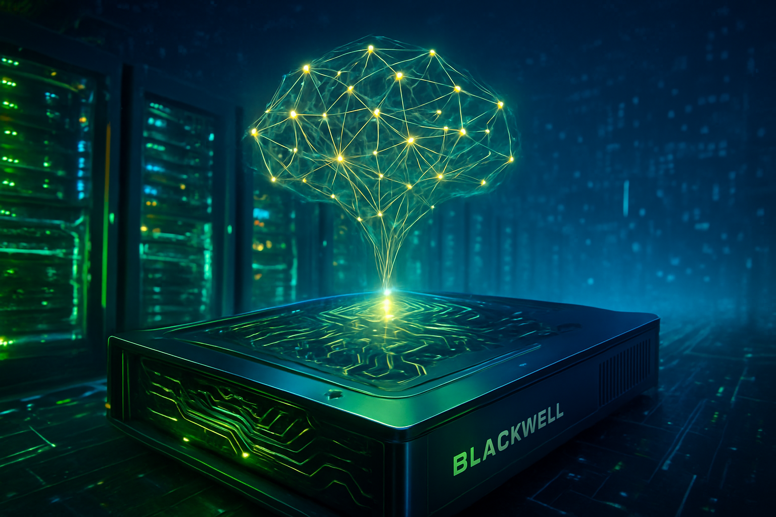
As 2025 draws to a close, the technology landscape looks fundamentally different than it did just twelve months ago. The catalyst for this transformation was the January 2025 launch of Nvidia’s (NASDAQ: NVDA) Blackwell architecture, a release that signaled the end of the "GPU as a component" era and the beginning of the "AI platform" age. By delivering the computational muscle required to run trillion-parameter models with unprecedented energy efficiency, Blackwell has effectively democratized the most advanced forms of generative AI, moving them from experimental labs into the heart of global enterprise and consumer hardware.
The arrival of the Blackwell B200 and the consumer-grade GeForce RTX 50-series in early 2025 addressed the most significant bottleneck in the industry: the "inference wall." Before Blackwell, running models with over a trillion parameters—the scale required for true reasoning and multi-modal agency—was prohibitively expensive and power-hungry. Today, as we look back on a year of rapid deployment, Nvidia’s strategic pivot toward system-level scaling has solidified its position as the foundational architect of the intelligence economy.
Engineering the Trillion-Parameter Powerhouse
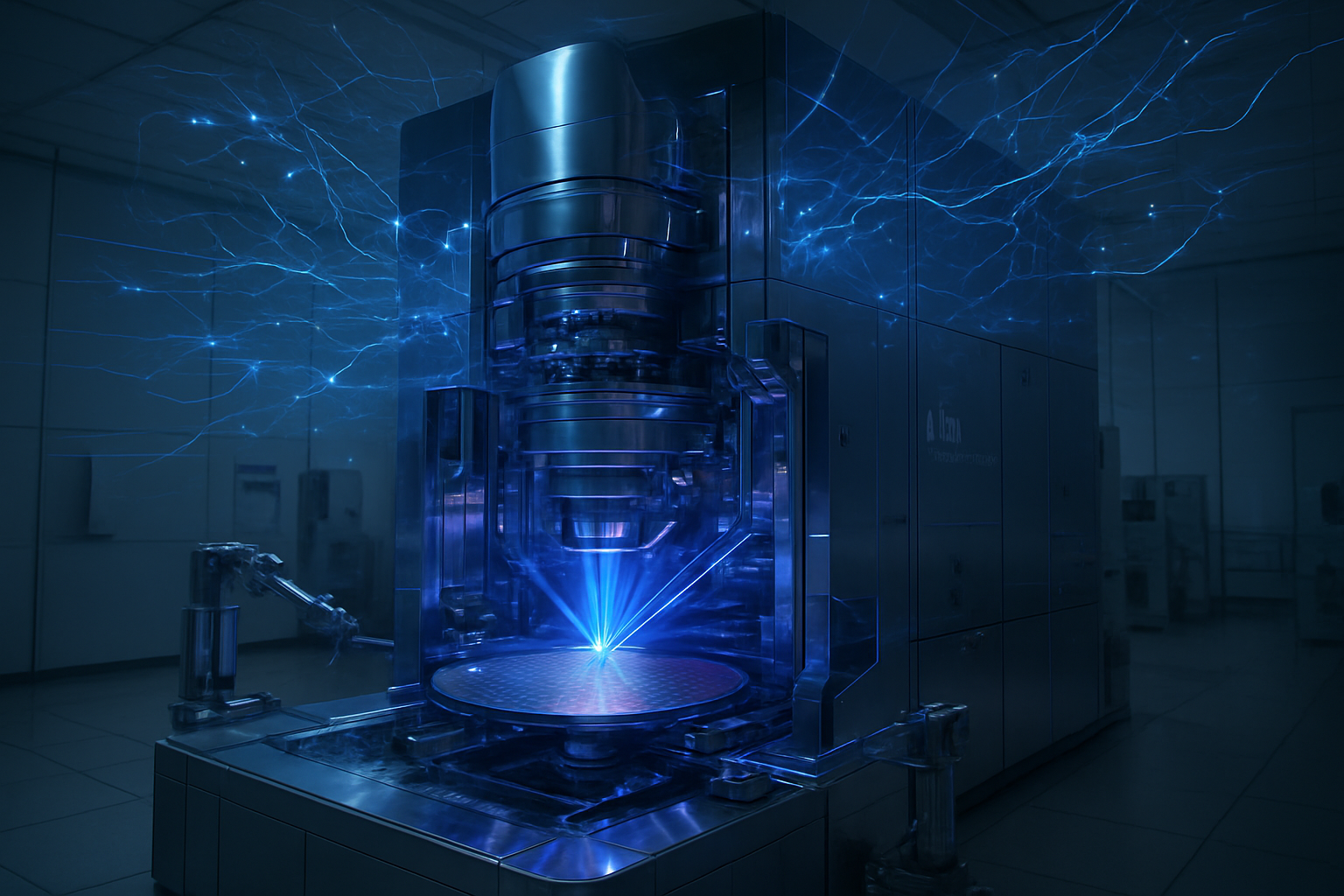
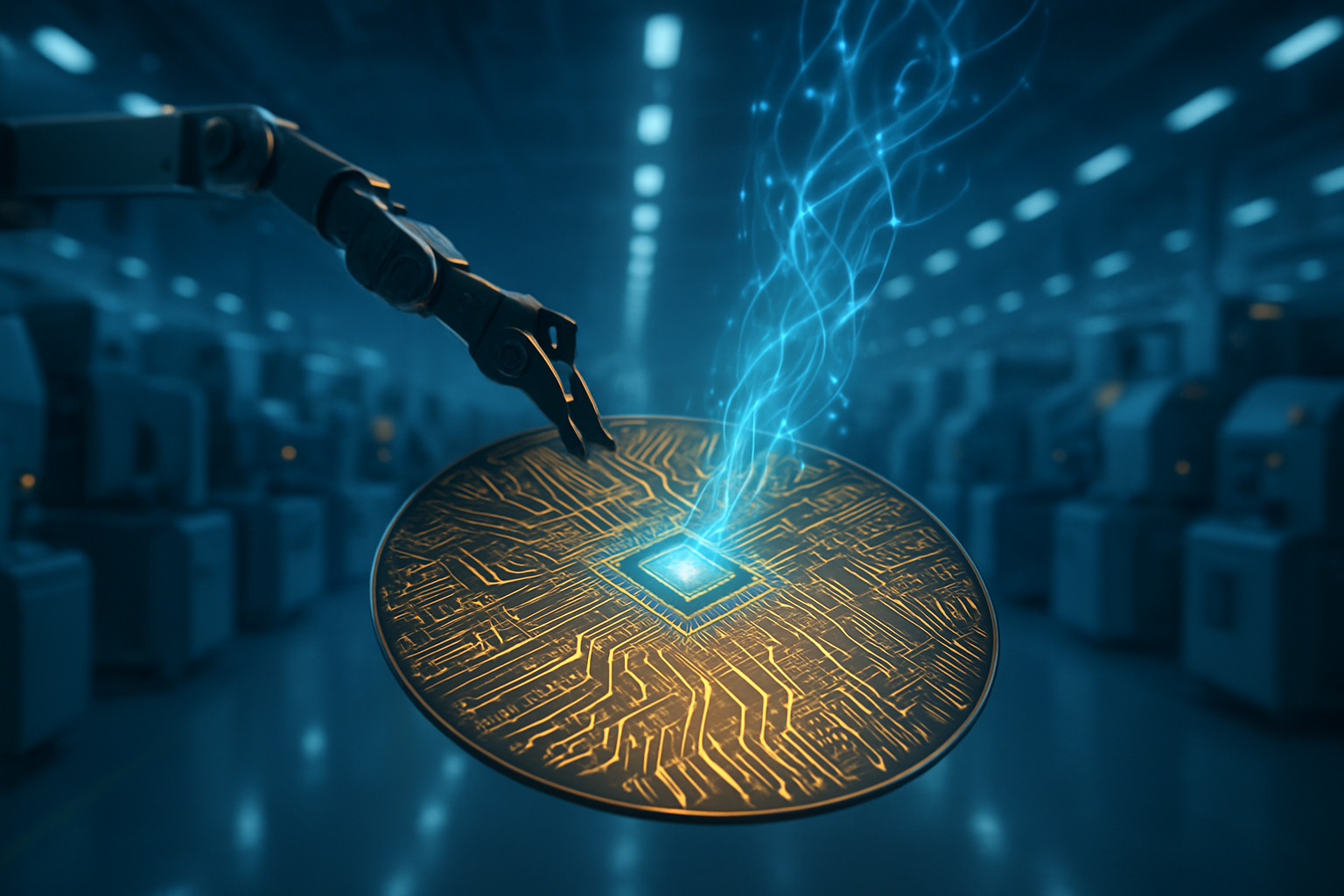
The technical cornerstone of the Blackwell architecture is the B200 GPU, a marvel of silicon engineering featuring 208 billion transistors. Unlike its predecessor, the H100, the B200 utilizes a multi-die design connected by a 10 TB/s chip-to-chip interconnect, allowing it to function as a single, massive unified processor. This is complemented by the second-generation Transformer Engine, which introduced support for FP4 and FP6 precision. These lower-bit formats have been revolutionary, allowing AI researchers to compress massive models to fit into memory with negligible loss in accuracy, effectively tripling the throughput for the latest Large Language Models (LLMs).
For the consumer and "prosumer" markets, the January 30, 2025, launch of the GeForce RTX 5090 and RTX 5080 brought this architecture to the desktop. The RTX 5090, featuring 32GB of GDDR7 VRAM and a staggering 3,352 AI TOPS (Tera Operations Per Second), has become the gold standard for local AI development. Perhaps most significant for the average user was the introduction of DLSS 4. By replacing traditional convolutional neural networks with a Vision Transformer architecture, DLSS 4 can generate three AI frames for every one native frame, providing a 4x boost in performance that has redefined high-end gaming and real-time 3D rendering.
The industry's reaction to these specs was immediate. Research labs noted that the GB200 NVL72—a liquid-cooled rack containing 72 Blackwell GPUs—delivers up to 30x faster real-time inference for 1.8-trillion parameter models compared to the previous Hopper-based systems. This leap allowed companies to move away from simple chatbots toward "agentic" AI systems capable of long-term planning and complex problem-solving, all while reducing the total cost of ownership by nearly 25x for inference tasks.
A New Hierarchy in the AI Arms Race
The launch of Blackwell has intensified the competitive dynamics among "hyperscalers" and AI startups alike. Major cloud providers, including Microsoft (NASDAQ: MSFT), Alphabet (NASDAQ: GOOGL), and Amazon (NASDAQ: AMZN), moved aggressively to integrate Blackwell into their data centers. By mid-2025, Oracle (NYSE: ORCL) and specialized AI cloud provider CoreWeave were among the first to offer "live" Blackwell instances, giving them a temporary but crucial edge in attracting high-growth AI startups that required the highest possible compute density for training next-generation models.
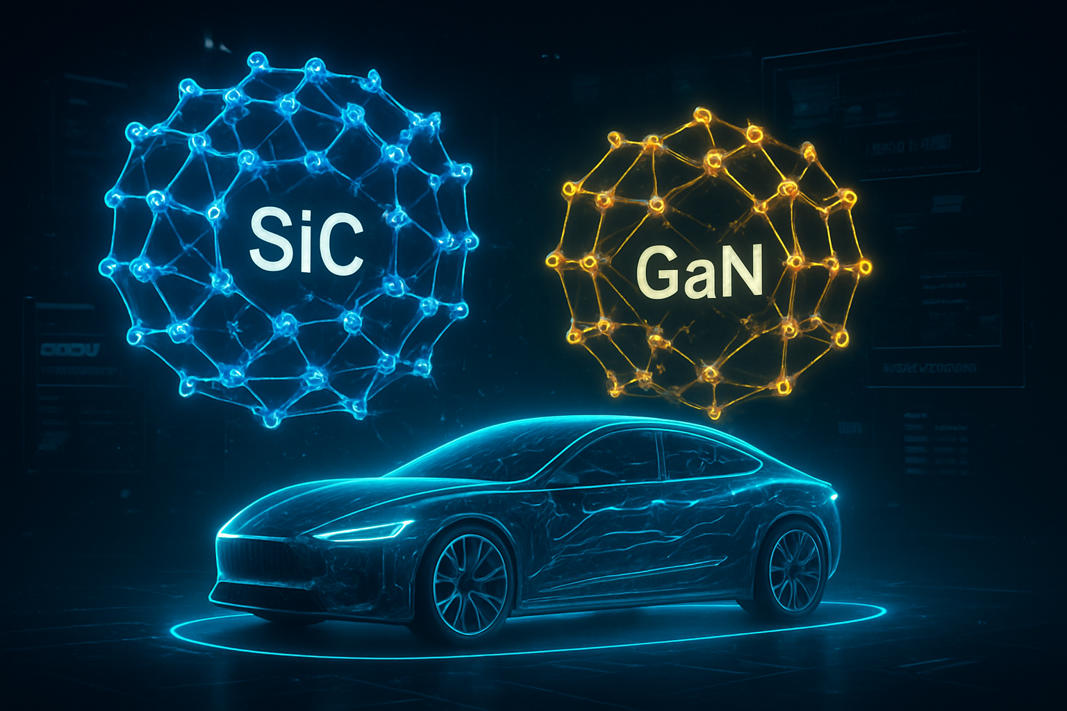
Beyond the cloud giants, the Blackwell architecture has disrupted the automotive and robotics sectors. Companies like Tesla (NASDAQ: TSLA) and various humanoid robot developers have leveraged the Blackwell-based GR00T foundation models to accelerate real-time imitation learning. The ability to process massive amounts of sensor data locally with high energy efficiency has turned Blackwell into the "brain" of the 2025 robotics boom. Meanwhile, competitors like Advanced Micro Devices (NASDAQ: AMD) and Intel (NASDAQ: INTC) have been forced to accelerate their own roadmaps, focusing on open-source software stacks to counter Nvidia's proprietary NVLink and CUDA dominance.
The market positioning of the RTX 50-series has also created a new tier of "local AI" power users. With the RTX 5090's massive VRAM, small-to-medium enterprises (SMEs) are now fine-tuning 70B and 100B parameter models in-house rather than relying on expensive, privacy-compromising cloud APIs. This shift toward "Hybrid AI"—where prototyping happens on a 50-series desktop and scaling happens on Blackwell cloud clusters—has become the standard workflow for the modern developer.
The Green Revolution and Sovereign AI
Perhaps the most significant long-term impact of the Blackwell launch is its contribution to "Green AI." In a year where energy consumption by data centers became a major political and environmental flashpoint, Nvidia’s focus on efficiency proved timely. Blackwell offers a 25x reduction in energy consumption for LLM inference compared to the Hopper architecture. This efficiency is largely driven by the transition to liquid cooling in the NVL72 racks, which has allowed data centers to triple their compute density without a corresponding spike in power usage or cooling costs.
This efficiency has also fueled the rise of "Sovereign AI." Throughout 2025, nations such as South Korea, India, and various European states have invested heavily in national AI clouds powered by Blackwell hardware. These initiatives aim to host localized models that reflect domestic languages and cultural nuances, ensuring that the benefits of the trillion-parameter era are not concentrated solely in Silicon Valley. By providing a platform that is both powerful and energy-efficient enough to be hosted within national power grids, Nvidia has become an essential partner in global digital sovereignty.
Comparing this to previous milestones, Blackwell is often cited as the "GPT-4 moment" of hardware. Just as GPT-4 proved that scaling models could lead to emergent reasoning, Blackwell has proved that scaling systems can make those emergent capabilities economically viable. However, this has also raised concerns regarding the "Compute Divide," where the gap between those who can afford Blackwell clusters and those who cannot continues to widen, potentially centralizing the most powerful AI capabilities in the hands of a few ultra-wealthy corporations and states.
Looking Toward the Rubin Architecture and Beyond
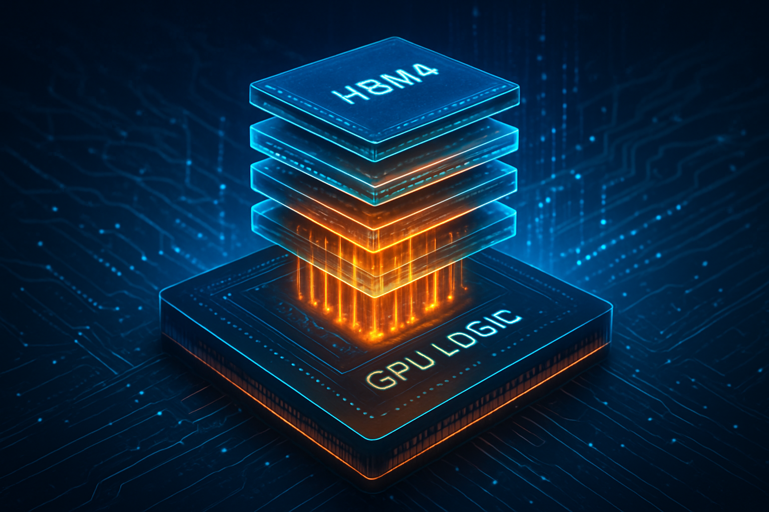
As we move into 2026, the focus is already shifting toward Nvidia's next leap: the Rubin architecture. While Blackwell focused on mastering the trillion-parameter model, early reports suggest that Rubin will target "World Models" and physical AI, integrating even more advanced HBM4 memory and a new generation of optical interconnects to handle the data-heavy requirements of autonomous systems.
In the near term, we expect to see the full rollout of "Project Digits," a rumored personal AI supercomputer that utilizes Blackwell-derived chips to bring data-center-grade inference to a consumer form factor. The challenge for the coming year will be software optimization; as hardware capacity has exploded, the industry is now racing to develop software frameworks that can fully utilize the FP4 precision and multi-die architecture of the Blackwell era. Experts predict that the next twelve months will see a surge in "small-but-mighty" models that use Blackwell’s specialized engines to outperform much larger models from the previous year.
Reflections on a Pivotal Year
The January 2025 launch of Blackwell and the RTX 50-series will likely be remembered as the moment the AI revolution became sustainable. By solving the dual challenges of massive model complexity and runaway energy consumption, Nvidia has provided the infrastructure for the next decade of digital growth. The key takeaways from 2025 are clear: the future of AI is multi-die, it is energy-efficient, and it is increasingly local.
As we enter 2026, the industry will be watching for the first "Blackwell-native" models—AI systems designed from the ground up to take advantage of FP4 precision and the NVLink 5 interconnect. While the hardware battle for 2025 has been won, the race to define what this unprecedented power can actually achieve is only just beginning.
This content is intended for informational purposes only and represents analysis of current AI developments.
TokenRing AI delivers enterprise-grade solutions for multi-agent AI workflow orchestration, AI-powered development tools, and seamless remote collaboration platforms.
For more information, visit https://www.tokenring.ai/.