San Francisco, CA – December 16, 2025 – OpenAI has officially launched GPT Image 1.5, its latest and most advanced image generation model, marking a significant leap forward in the capabilities of generative artificial intelligence. Released today, December 16, 2025, this new iteration is now integrated into ChatGPT and accessible via its API, promising unprecedented speed, precision, and control over visual content creation. The announcement intensifies the already fierce competition in the AI image generation landscape, particularly against rivals like Google (NASDAQ: GOOGL), and is poised to reshape how creative professionals and businesses approach visual design and content production.
GPT Image 1.5 arrives as a direct response to the accelerating pace of innovation in multimodal AI, aiming to set a new benchmark for production-quality visuals and highly controllable creative workflows. Its immediate significance lies in its potential to democratize sophisticated image creation, making advanced AI-driven editing and generation tools available to a broader audience while simultaneously pushing the boundaries of what is achievable in terms of realism, accuracy, and efficiency in AI-generated imagery.
Technical Prowess and Competitive Edge
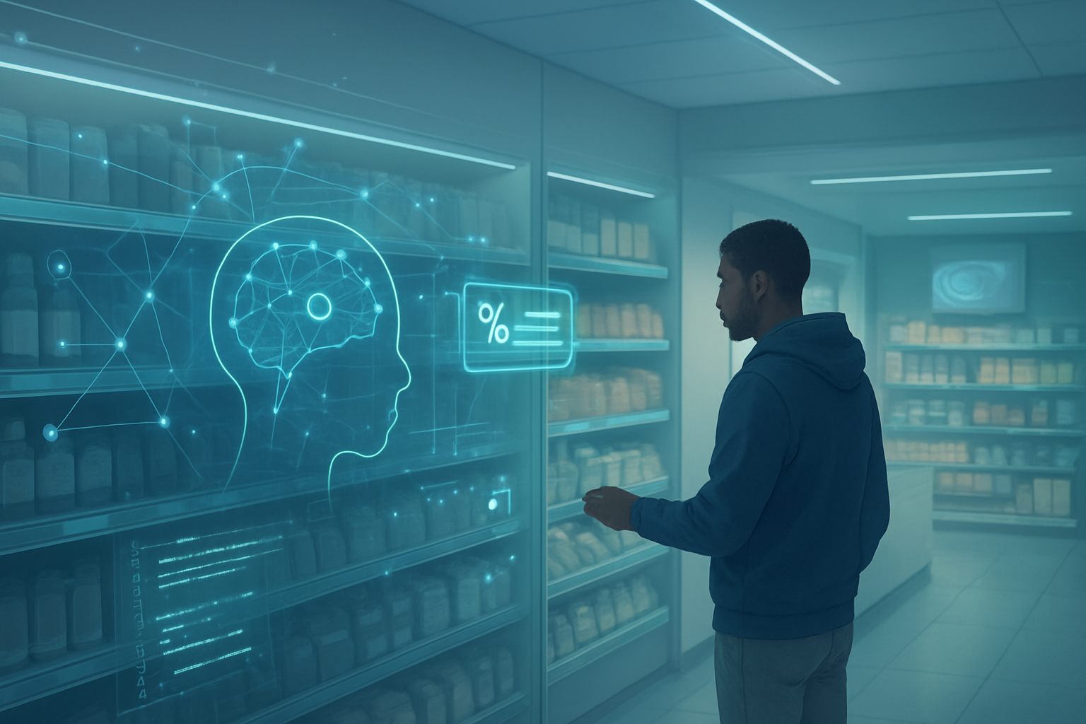
GPT Image 1.5 builds upon OpenAI's previous efforts, succeeding the GPT Image 1 model, with a focus on delivering major improvements across several critical areas. Technically, the model boasts up to four times faster image generation, drastically cutting down feedback cycles for users. Its core strength lies in its precise editing capabilities, allowing for granular control to add, subtract, combine, blend, and transpose elements within images. Crucially, it is engineered to maintain details such as lighting, composition, and facial appearance during edits, ensuring consistency that was often a challenge in earlier models where minor tweaks could lead to a complete reinterpretation of the image.
A standout feature is GPT Image 1.5's enhanced instruction following, demonstrating superior adherence to user prompts and complex directives, which translates into more accurate and desired outputs. Furthermore, it exhibits significantly improved text rendering within generated images, handling denser and smaller text with greater reliability—a critical advancement for applications requiring legible text in visuals. For developers, OpenAI (NASDAQ: OPENAI) has made GPT Image 1.5 available through its API at a 20% reduced cost for image inputs and outputs compared to its predecessor, gpt-image-1, making high-quality image generation more accessible for a wider range of applications and businesses. The model also introduces a dedicated "Images" interface within ChatGPT, offering a more intuitive "creative studio" experience with preset filters and trending prompts.
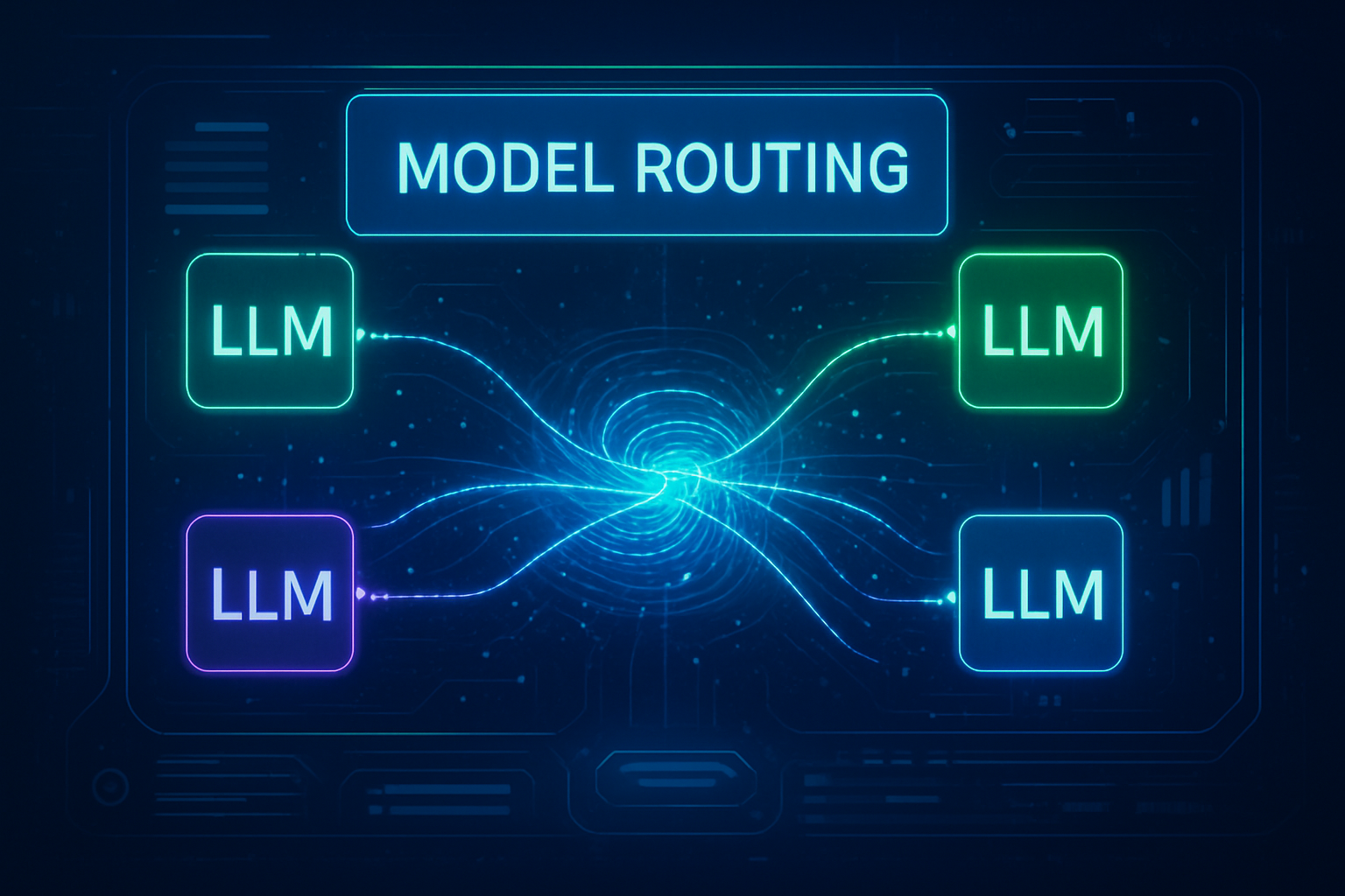
This release directly challenges Google's formidable Gemini image generation models, specifically Gemini 2.5 Flash Image (codenamed "Nano Banana"), launched in August 2025, and Gemini 3 Pro Image (codenamed "Nano Banana Pro"), released in November 2025. While Google's models were lauded for multi-image fusion, character consistency, and advanced visual design, GPT Image 1.5 emphasizes superior instruction adherence, precise detail preservation for logos and faces, and enhanced text rendering. Nano Banana Pro, in particular, offers higher resolution outputs (up to 4K) and multilingual text rendering with a variety of stylistic options, along with SynthID watermarking for provenance—a feature not explicitly detailed for GPT Image 1.5. However, GPT Image 1.5's speed and cost-effectiveness for API users present a strong counter-argument. Initial reactions from the AI research community and industry experts highlight GPT Image 1.5's potential as a "game-changer" for professionals due to its realism, text integration, and refined editing, intensifying the "AI arms race" in multimodal capabilities.
Reshaping the AI Industry Landscape
The introduction of GPT Image 1.5 is set to profoundly impact AI companies, tech giants, and startups alike. OpenAI (NASDAQ: OPENAI) itself stands to solidify its leading position in the generative AI space, enhancing its DALL-E product line and attracting more developers and enterprise clients to its API services. This move reinforces its ecosystem and demonstrates continuous innovation, strategically positioning it against competitors. Cloud computing providers like Amazon (AWS), Microsoft (Azure), and Google Cloud will see increased demand for computational resources, while hardware manufacturers, particularly those producing advanced GPUs such as NVIDIA (NASDAQ: NVDA), will experience a surge in demand for their specialized AI accelerators. Creative industries, including marketing, advertising, gaming, and entertainment, are poised to benefit immensely from accelerated content creation and reduced costs.
For tech giants like Google (NASDAQ: GOOGL), the release intensifies the competitive pressure. Google will likely accelerate its internal research and development, potentially fast-tracking an equivalent or superior model, or focusing on differentiating factors like integration with its extensive cloud services and Android ecosystem. The competition could also spur Google to acquire promising AI image startups or invest heavily in specific application areas.
Startups in the AI industry face both significant challenges and unprecedented opportunities. Those building foundational image generation models will find it difficult to compete with OpenAI's resources. However, application-layer startups focusing on specialized tools for content creation, e-commerce (e.g., AI-powered product visualization), design, architecture, education, and accessibility stand to benefit significantly. These companies can thrive by building unique user experiences and domain-specific workflows on top of GPT Image 1.5's core capabilities, much like software companies build on cloud infrastructure. This development could disrupt traditional stock photo agencies by reducing demand for generic imagery and force graphic design tools like Adobe Photoshop (NASDAQ: ADBE) and Canva to innovate on advanced editing, collaborative features, and professional workflows, rather than competing directly on raw image generation. Entry-level design services might also face increased competition from AI-powered tools enabling clients to generate their own assets.
Wider Significance and Societal Implications
GPT Image 1.5 fits seamlessly into the broader AI landscape defined by the dominance of multimodal AI, the rise of agentic AI, and continuous advancements in self-training and inference scaling. By December 2025, AI is increasingly integrated into everyday applications, and GPT Image 1.5 will accelerate this trend, becoming an indispensable tool across various sectors. Its enhanced capabilities will revolutionize content creation, marketing, research and development, and education, enabling faster, more efficient, and hyper-personalized visual content generation. It will also foster the emergence of new professional roles such as "prompt engineers" and "AI directors" who can effectively leverage these advanced tools.
However, this powerful technology amplifies existing ethical and societal concerns. The ability to generate highly realistic images exacerbates the risk of misinformation and deepfakes, potentially impacting public trust and individual reputations. If trained on biased datasets, GPT Image 1.5 could perpetuate and amplify societal biases. Questions of copyright and intellectual property for AI-generated content will intensify, and concerns about data privacy, job displacement for visual content creators, and the environmental impact of training large models remain paramount. Over-reliance on AI might also diminish human creativity and critical thinking, highlighting the need for clear accountability.
Comparing GPT Image 1.5 to previous AI milestones reveals its evolutionary significance. It surpasses early image generation efforts like GANs, DALL-E 1, Midjourney, and Stable Diffusion by offering more nuanced control, higher fidelity, and deeper contextual understanding, moving beyond simple text-to-image synthesis. While GPT-3 and GPT-4 brought breakthroughs in language understanding and multimodal input, GPT Image 1.5 is distinguished by its native and advanced image generation capabilities, producing sophisticated visuals with high precision. In the context of cutting-edge multimodal models like Google's Gemini and OpenAI's GPT-4o, GPT Image 1.5 signifies a specialized iteration that pushes the boundaries of visual generation and manipulation beyond general multimodal capabilities, offering unparalleled control over image details and creative elements.
The Road Ahead: Future Developments and Challenges
In the near term, following the release of GPT Image 1.5, expected developments will focus on further refining its core strengths. This includes even more precise instruction following and editing, perfecting text rendering within images for diverse applications, and advanced multi-turn and contextual understanding to maintain coherence across ongoing visual conversations. Seamless multimodal integration will deepen, enabling the generation of comprehensive content that combines various media types effortlessly.
Longer term, experts predict a future where multimodal AI systems like GPT Image 1.5 evolve to possess emotional intelligence, capable of interpreting tone and mood for more human-like interactions. This will pave the way for sophisticated AI-powered companions, unified work assistants, and next-generation search engines that dynamically combine images, voice, and written queries. The vision extends to advanced generative AI for video and 3D content, pushing the boundaries of digital art and immersive experiences, with models like OpenAI's Sora already demonstrating early potential in video generation.
Potential applications span creative industries (advertising, fashion, art, visual storytelling), healthcare (medical imaging analysis, drug discovery), e-commerce (product image generation, personalized recommendations), education (rich, illustrative content), accessibility (real-time visual descriptions), human-computer interaction, and security (image recognition and content moderation).
However, significant challenges remain. Data alignment and synchronization across different modalities, computational costs, and model complexity for robust generalization are technical hurdles. Ensuring data quality and consistency, mitigating bias, and addressing ethical considerations are crucial for responsible deployment. Furthermore, bridging the gap between flexible generation and reliable, precise control, along with fostering transparency about model architectures and training data, are essential for the continued progress and societal acceptance of such powerful AI systems. Gartner predicts that 40% of generative AI solutions will be multimodal by 2027, underscoring the rapid shift towards integrated AI experiences. Experts also foresee the rise of "AI teammates" across business functions and accelerated enterprise adoption of generative AI in 2025.
A New Chapter in AI History
The release of OpenAI's GPT Image 1.5 on December 16, 2025, marks a pivotal moment in the history of artificial intelligence. It represents a significant step towards the maturation of generative AI, particularly in the visual domain, by consolidating multimodal capabilities, advancing agentic intelligence, and pushing the boundaries of creative automation. Its enhanced speed, precision editing, and improved text rendering capabilities promise to democratize high-quality image creation and empower professionals across countless industries.
The immediate weeks and months will be crucial for observing the real-world adoption and impact of GPT Image 1.5. We will be watching for how quickly developers integrate its API, the innovative applications that emerge, and the competitive responses from other tech giants. The ongoing dialogue around ethical AI, copyright, and job displacement will intensify, necessitating thoughtful regulation and responsible development. Ultimately, GPT Image 1.5 is not just another model release; it's a testament to the relentless pace of AI innovation and a harbinger of a future where AI becomes an even more indispensable creative and analytical partner, reshaping our visual world in profound ways.
This content is intended for informational purposes only and represents analysis of current AI developments.
TokenRing AI delivers enterprise-grade solutions for multi-agent AI workflow orchestration, AI-powered development tools, and seamless remote collaboration platforms.
For more information, visit https://www.tokenring.ai/.