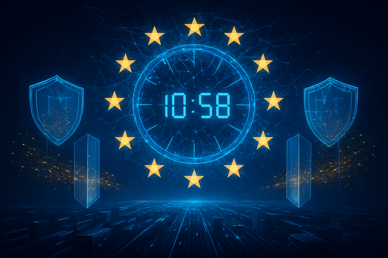
SACRAMENTO, CA — As of January 1, 2026, the digital landscape in California has undergone a fundamental shift. California Senate Bill 942 (SB 942), officially known as the California AI Transparency Act, is now in full effect, marking the most aggressive effort by any U.S. state to combat the rising tide of deepfakes and synthetic media. The law mandates that large-scale artificial intelligence providers—those with over one million monthly users—must now provide clear disclosures for AI-generated content and offer free, public tools to help users verify the provenance of digital media.
The implementation of SB 942 represents a watershed moment for the tech industry. By requiring a "cryptographic fingerprint" to be embedded in images, video, and audio, California is attempting to build a standardized infrastructure for truth in an era where seeing is no longer believing. As of January 5, 2026, major AI labs have already begun rolling out updated interfaces and public APIs to comply with the new mandates, even as a looming legal battle with federal authorities threatens to complicate the rollout.
The Technical Architecture of Trust: Watermarks and Detection APIs
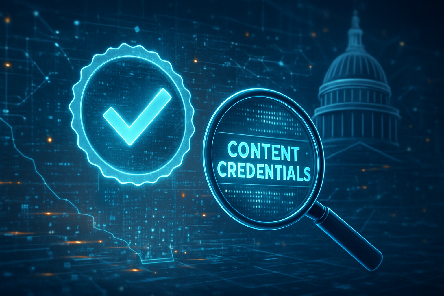
At the heart of SB 942 are two distinct types of disclosures: latent and manifest. Latent disclosures are invisible, "extraordinarily difficult to remove" metadata embedded directly into the file's code. This metadata must include the provider’s name, the AI system’s version, the timestamp of creation, and a unique identifier. Manifest disclosures, conversely, are visible watermarks or icons that a user can choose to include, providing an immediate visual cue that the content was synthesized. This dual-layered approach is designed to ensure that even if a visible watermark is cropped out, the underlying data remains intact for verification.
To facilitate this, the law leans heavily on the C2PA (Coalition for Content Provenance and Authenticity) standard. This industry-wide framework, championed by companies like Adobe Inc. (NASDAQ:ADBE) and Microsoft Corp. (NASDAQ:MSFT), uses cryptographically signed "Content Credentials" to track a file's history. Unlike previous voluntary efforts, SB 942 makes this technical standard a legal necessity for any major provider operating in California. Furthermore, providers are now legally required to offer a free, publicly accessible URL-based tool and an API that allows third-party platforms—such as social media networks—to instantly query whether a specific piece of media originated from their system.
This technical mandate differs significantly from previous "best effort" approaches. Earlier watermarking techniques were often easily defeated by simple compression or screenshots. SB 942 raises the bar by requiring that disclosures remain functional through common editing processes. Initial reactions from the AI research community have been cautiously optimistic, though some experts warn that the "arms race" between watermarking and removal tools will only intensify. Researchers at Stanford’s Internet Observatory noted that while the law provides a robust framework, the "provenance gap"—the ability of sophisticated actors to strip metadata—remains a technical hurdle that the law’s "technically feasible" clause will likely test in court.
Market Bifurcation: Tech Giants vs. Emerging Startups
The economic impact of SB 942 is already creating a two-tier market within the AI sector. Tech giants like Alphabet Inc. (NASDAQ:GOOGL) and Meta Platforms Inc. (NASDAQ:META) were largely prepared for the January 1 deadline, having integrated C2PA standards into their generative tools throughout 2025. For these companies, compliance is a manageable operational cost that doubles as a competitive advantage, allowing them to market their models as "safety-first" and "legally compliant" for enterprise clients who fear the liability of un-watermarked content.
In contrast, mid-sized startups and "scalers" approaching the one-million-user threshold are feeling the "compliance drag." The requirement to host a free, high-uptime detection API and manage the legal risks of third-party licensing is a significant burden. Under SB 942, if an AI provider discovers that a licensee—such as a smaller app using their API—is stripping watermarks, the provider must revoke the license within 96 hours or face civil penalties of $5,000 per violation, per day. This "policing" requirement is forcing startups to divert up to 20% of their R&D budgets toward compliance and legal teams, potentially slowing the pace of innovation for smaller players.
Strategic positioning is already shifting in response. Some smaller firms are opting to remain under the one-million-user cap or are choosing to build their applications on top of compliant "big tech" APIs rather than developing proprietary models. This "platformization" could inadvertently consolidate power among the few companies that can afford the robust transparency infrastructure required by California law. Meanwhile, companies like Adobe are capitalizing on the shift, offering "Provenance-as-a-Service" tools to help smaller developers meet the state's rigorous technical mandates.
A Global Standard or a Federal Flashpoint?
The significance of SB 942 extends far beyond the borders of California. As the fifth-largest economy in the world, California’s regulations often become the de facto national standard—a phenomenon known as the "California Effect." The law is more prescriptive than the EU AI Act, which focuses on a broader risk-based approach but is less specific about the technical metadata required for multimedia. While the EU mandates that AI-generated text be identifiable, SB 942 focuses specifically on the "high-stakes" media of audio, video, and images, creating a more targeted but technically deeper transparency regime.
However, the law has also become a focal point for federal tension. In December 2025, the Trump Administration established an "AI Litigation Task Force" aimed at rolling out a "minimally burdensome" federal framework for AI. The administration has signaled its intent to challenge SB 942 on the grounds of federal preemption, arguing that a patchwork of state laws interferes with interstate commerce. This sets the stage for a major constitutional showdown between California Attorney General Rob Bonta and federal regulators, with the future of state-led AI safety hanging in the balance.
Potential concerns remain regarding the "text exemption" in SB 942. Currently, the law does not require disclosures for AI-generated text, a decision made during the legislative process to avoid First Amendment challenges and technical difficulties in watermarking prose. Critics argue that this leaves a massive loophole for AI-driven disinformation campaigns that rely on text-based "fake news" articles. Despite this, the law's focus on deepfake images and videos addresses the most immediate and visceral threats to public trust and election integrity.
The Horizon: From Watermarks to Verified Reality
Looking ahead, the next 12 to 24 months will likely see an evolution in both the technology and the scope of transparency laws. Experts predict that if SB 942 survives its legal challenges, the next frontier will be "authenticated capture"—technology built directly into smartphone cameras that signs "real" photos at the moment of creation. This would shift the burden from identifying what is fake to verifying what is real. We may also see future amendments to SB 942 that expand its reach to include text-based generative AI as watermarking techniques for LLMs (Large Language Models) become more sophisticated.
In the near term, the industry will be watching for the first "notice of violation" letters from the California Attorney General’s office. These early enforcement actions will define what "technically feasible" means in practice. If a company's watermark is easily removed by a third-party tool, will the provider be held liable? The answer to that question will determine whether SB 942 becomes a toothless mandate or a powerful deterrent against the malicious use of synthetic media.
Conclusion: A Landmark in AI Governance
California’s SB 942 is more than just a regulatory hurdle; it is a fundamental attempt to re-establish the concept of provenance in a post-truth digital environment. By mandating that the largest AI providers take responsibility for the content their systems produce, the law shifts the burden of proof from the consumer to the creator. The key takeaways for the industry are clear: transparency is no longer optional, and technical standards like C2PA are now the bedrock of AI development.
As we move deeper into 2026, the success of the AI Transparency Act will be measured not just by the number of watermarks, but by the resilience of our information ecosystem. While the legal battle with the federal government looms, California has successfully forced the world’s most powerful AI companies to build the tools necessary for a more honest internet. For now, the tech industry remains in a state of high alert, balancing the drive for innovation with the new, legally mandated reality of total transparency.
This content is intended for informational purposes only and represents analysis of current AI developments.
TokenRing AI delivers enterprise-grade solutions for multi-agent AI workflow orchestration, AI-powered development tools, and seamless remote collaboration platforms.
For more information, visit https://www.tokenring.ai/.