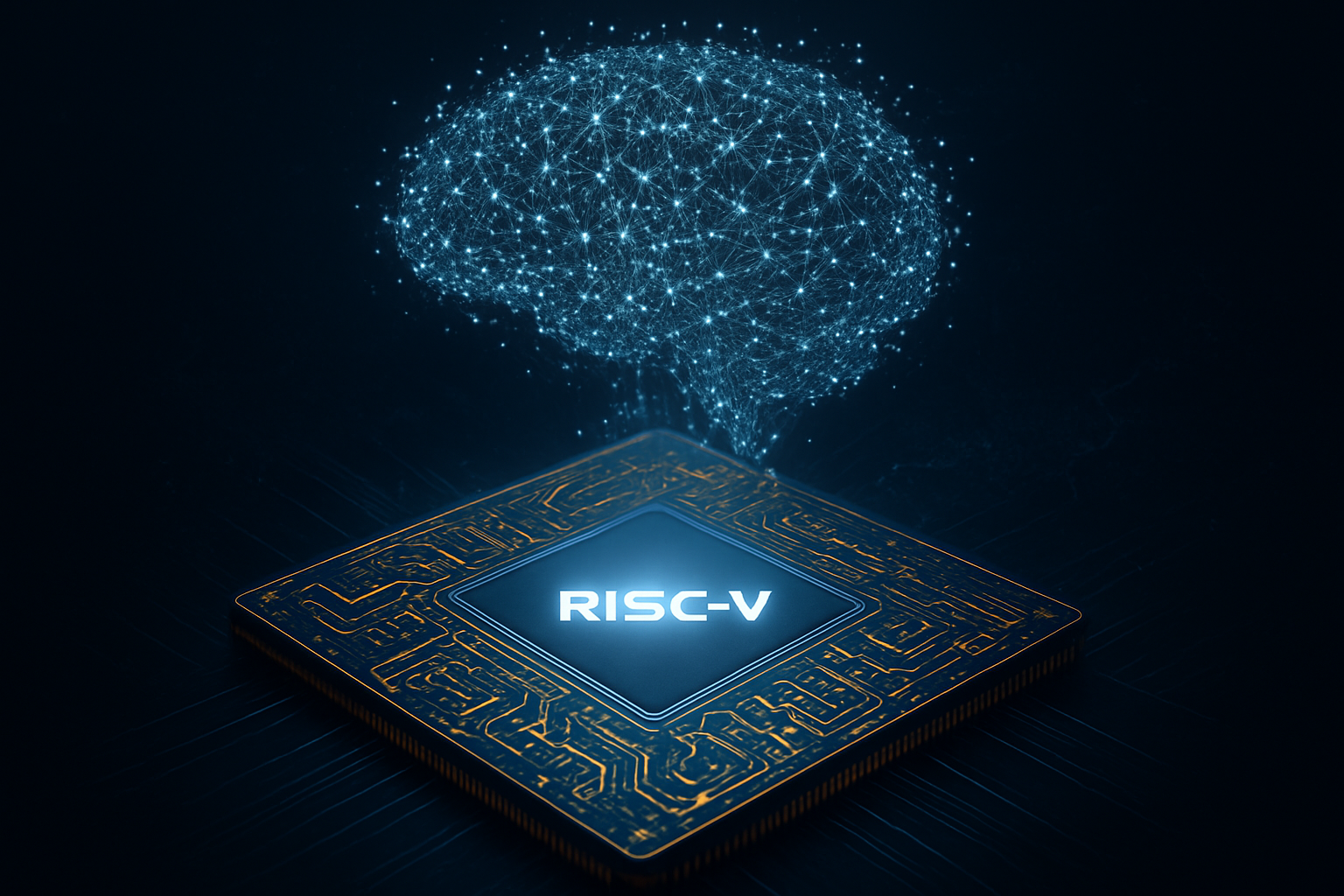
Tag: TechNews

  • The Great Memory Crunch: Why AI’s Insatiable Hunger for HBM is Starving the Global Tech Market

    The Great Memory Crunch: Why AI’s Insatiable Hunger for HBM is Starving the Global Tech Market

    As we move deeper into 2026, the global technology landscape is grappling with a "structural crisis" in memory supply that few predicted would be this severe. The pivot toward High Bandwidth Memory (HBM) to power generative AI is no longer just a corporate strategy; it has become a disruptive force that is cannibalizing the production of traditional DRAM and NAND. With the world’s leading chipmakers—Samsung Electronics (KRX: 005930), SK Hynix (KRX: 000660), and Micron Technology (NASDAQ: MU)—reporting that their HBM capacity is fully booked through the end of 2026, the downstream effects are beginning to hit consumer wallets.

    This unprecedented shift has triggered a "supercycle" of rising prices for smartphones, laptops, and enterprise hardware. As manufacturers divert their most advanced fabrication lines to fulfill massive orders from AI giants like NVIDIA (NASDAQ: NVDA), the "commodity" memory used in everyday devices is becoming increasingly scarce. We are now entering a two-year window where the cost of digital storage and processing power may rise for the first time in a decade, fundamentally altering the economics of the consumer electronics industry.

    The 1:3 Penalty: The Technical Bottleneck of AI Memory

    The primary driver of this shortage is a harsh technical reality known in the industry as the "1:3 Capacity Penalty." Unlike standard DDR5 memory, which is produced on a single horizontal plane, HBM is a complex 3D structure that stacks 12 to 16 DRAM dies vertically. To produce a single HBM wafer, manufacturers must sacrifice the equivalent of approximately three standard DDR5 wafers. This is due to the larger physical footprint of HBM dies and the significantly lower yields associated with the vertical stacking process. While a standard DRAM line might see yields exceeding 90%, the extreme precision required for Through-Silicon Vias (TSVs)—thousands of microscopic holes drilled through the silicon—keeps HBM yields closer to 65%.

    Furthermore, the transition to HBM4 in early 2026 has introduced a new layer of complexity. For the first time, memory manufacturers are integrating "foundry-logic" dies at the base of the memory stack, often requiring partnerships with specialized foundries like TSMC (TPE: 2330). This shift from a pure memory product to a hybrid logic-memory component has slowed production cycles and increased the "cleanroom footprint" required for each unit of output. As the industry moves toward 16-layer HBM4 stacks later this year, the thinning of silicon dies to just 30 micrometers—about a third the thickness of a human hair—has made the manufacturing process even more volatile.

    Initial reactions from industry analysts suggest that we are witnessing the end of "cheap memory." Experts from Gartner and TrendForce have noted that the divergence in manufacturing is creating a tiered silicon market. While AI data centers are receiving the latest HBM4 innovations, the consumer PC and mobile markets are being forced to survive on "scraps" from older, less efficient production lines. The industry’s focus has shifted entirely from maximizing volume to maximizing high-margin, high-complexity AI components.

    A Zero-Sum Game for the Silicon Giants

    The competitive landscape of 2026 has become a high-stakes race for HBM dominance, leaving little room for the traditional DRAM business. SK Hynix (KRX: 000660) continues to hold a commanding lead, controlling over 50% of the HBM market. Their early bet on mass-producing 12-layer HBM3E has paid off, as they have secured the vast majority of NVIDIA's (NASDAQ: NVDA) orders for the current fiscal year. Samsung Electronics (KRX: 005930), meanwhile, is aggressively playing catch-up, repurposing vast sections of its P4 fab in Pyeongtaek to HBM production, effectively reducing its output of mobile LPDDR5X RAM by nearly 30% in the process.

    Micron Technology (NASDAQ: MU) has also joined the fray, focusing on energy-efficient HBM3E for edge AI applications. However, the surge in demand from "Big Tech" firms like Google (NASDAQ: GOOGL) and Meta (NASDAQ: META) has led to a situation where these three suppliers have zero unallocated capacity for the next 20 months. For major AI labs and hyperscalers, this means their growth is limited not by software or capital, but by the physical availability of silicon. This has created a strategic advantage for those who signed "Long-Term Agreements" (LTAs) early in 2025, effectively locking out smaller startups and mid-tier server providers from the AI gold rush.

    This corporate pivot is causing significant disruption to traditional product roadmaps. Companies that rely on high-volume, low-cost memory—such as budget smartphone manufacturers and IoT device makers—are finding themselves at the back of the line. The market positioning has shifted: the big three memory makers are no longer just suppliers; they are now the gatekeepers of AI progress, and their preference for high-margin HBM contracts is starving the rest of the ecosystem.

    The "BOM Crisis" and the Rise of Spec Shrinkflation

    The wider significance of this memory drought is most visible in the rising "Bill of Materials" (BOM) for consumer devices. As of early 2026, the average selling price of a smartphone has climbed toward $465, a significant jump from previous years. Memory, which typically accounts for 10-15% of a device's cost, has seen spot prices for LPDDR5 and NAND flash increase by 60% since mid-2025. This is forcing PC manufacturers to engage in what analysts call "Spec Shrinkflation"—releasing new laptop models with 8GB or 12GB of RAM instead of the 16GB standard that was becoming the norm, just to keep price points stable.

    This trend is particularly problematic for Microsoft (NASDAQ: MSFT) and its "Copilot+" PC initiative, which mandates a minimum of 16GB of RAM for local AI processing. With 16GB modules in short supply, the price of "AI-ready" PCs is expected to rise by at least 8% by the end of 2026. This creates a paradox: the very AI revolution that is driving memory demand is also making the hardware required to run that AI too expensive for the average consumer.

    Concerns are also mounting regarding the inflationary impact on the broader economy. As memory is a foundational component of everything from cars to medical devices, the scarcity is rippling through sectors far removed from Silicon Valley. We are seeing a repeat of the 2021 chip shortage, but with a crucial difference: this time, the shortage is not caused by a supply chain breakdown, but by a deliberate shift in manufacturing priority toward the highest bidder—AI data centers.

    Looking Ahead: The Road to 2027 and HBM4E

    Looking toward 2027, the industry is preparing for the arrival of HBM4E, which promises even greater bandwidth but at the cost of even more complex manufacturing requirements. Near-term developments will likely focus on "Foundry-Memory" integration, where memory stacks are increasingly customized for specific AI chips. This bespoke approach will likely further reduce the supply of "generic" memory, as production lines become highly specialized for individual customers.

    Experts predict that the memory shortage will not ease until at least mid-2027, when new greenfield fabrication plants in Idaho and South Korea are expected to come online. Until then, the primary challenge will be balancing the needs of the AI industry with the survival of the consumer electronics market. We may see a shift toward "modular" memory designs in laptops to allow users to upgrade their own RAM, a trend that could reverse the years-long move toward soldered, non-replaceable components.

    A New Era of Silicon Scarcity

    The memory crisis of 2026-2027 represents a pivotal moment in the history of computing. It marks the transition from an era of silicon abundance to an era of strategic allocation. The key takeaway is clear: High Bandwidth Memory is the new oil of the digital economy, and its extraction comes at a high price for the rest of the tech world. Samsung, SK Hynix, and Micron have fundamentally changed their business models, moving away from the volatile commodity cycles of the past toward a more stable, high-margin future anchored by AI.

    For consumers and enterprise IT buyers, the next 24 months will be characterized by higher costs and difficult trade-offs. The significance of this development cannot be overstated; it is the first time in the modern era that the growth of one specific technology—Generative AI—has directly restricted the availability of basic computing resources for the global population. As we move into the second half of 2026, all eyes will be on whether manufacturing yields can improve fast enough to prevent a total stagnation in the consumer hardware market.


    This content is intended for informational purposes only and represents analysis of current AI developments.

    TokenRing AI delivers enterprise-grade solutions for multi-agent AI workflow orchestration, AI-powered development tools, and seamless remote collaboration platforms.
    For more information, visit https://www.tokenring.ai/.

  • Silicon Sovereignty: India’s Semiconductor Mission Hits Full Throttle as Commercial Production Begins in 2026

    Silicon Sovereignty: India’s Semiconductor Mission Hits Full Throttle as Commercial Production Begins in 2026

    As of January 21, 2026, the global semiconductor landscape has reached a definitive turning point. The India Semiconductor Mission (ISM), once viewed by skeptics as an ambitious but distant dream, has transitioned into a tangible industrial powerhouse. With a cumulative investment of Rs 1.60 lakh crore ($19.2 billion) fueling the domestic ecosystem, India has officially joined the elite ranks of semiconductor-producing nations. This milestone marks the shift from construction and planning to the active commercial rollout of "Made in India" chips, positioning the nation as a critical pillar in the global technology supply chain and a burgeoning hub for AI hardware.

    The immediate significance of this development cannot be overstated. As global demand for AI-optimized silicon, automotive electronics, and 5G infrastructure continues to surge, India’s entry into high-volume manufacturing provides a much-needed alternative to traditional East Asian hubs. By successfully operationalizing four major plants—led by industry giants like Tata Electronics and Micron Technology, Inc. (NASDAQ: MU)—India is not just securing its own digital future but is also offering global tech firms a resilient, geographically diverse production base to mitigate supply chain risks.

    From Blueprints to Silicon: The Technical Evolution of India’s Fab Landscape

    The technical cornerstone of this evolution is the Dholera "mega-fab" established by Tata Electronics in partnership with Powerchip Semiconductor Manufacturing Corp. (TWSE: 6770). As of January 2026, this $10.9 billion facility has initiated high-volume trial runs, processing 300mm wafers at nodes ranging from 28nm to 110nm. Unlike previous attempts at semiconductor manufacturing in the region, the Dholera plant utilizes state-of-the-art automated wafer handling and precision lithography systems tailored for the automotive and power management sectors. This shift toward mature nodes is a strategic calculation, addressing the most significant volume demands in the global market rather than competing immediately for the sub-5nm "bleeding edge" occupied by TSMC.

    Simultaneously, the advanced packaging sector has seen explosive growth. Micron Technology, Inc. (NASDAQ: MU) has officially moved its Sanand facility into full-scale commercial production this month, shipping high-density DRAM and NAND flash products to global markets. This facility is notable for its modular construction and advanced ATMP (Assembly, Testing, Marking, and Packaging) techniques, which have set a new benchmark for speed-to-market in the industry. Meanwhile, Tata’s Assam-based facility is preparing for mid-2026 pilot production, aiming for a staggering capacity of 48 million chips per day using Flip Chip and Integrated Systems Packaging technologies, which are essential for high-performance AI servers.

    Industry experts have noted that India’s approach differs from previous efforts through its focus on the "OSAT-first" (Outsourced Semiconductor Assembly and Test) strategy. By proving capability in testing and packaging before the full fabrication process is matured, India has successfully built a workforce and logistics network that can support the complex needs of modern silicon. This strategy has drawn praise from the international research community, which views India's rapid scale-up as a masterclass in industrial policy and public-private partnership.

    Competitive Landscapes and the New Silicon Silk Road

    The commercial success of these plants is creating a ripple effect across the public markets and the broader tech sector. CG Power and Industrial Solutions Ltd (NSE: CGPOWER), through its joint venture with Renesas Electronics Corporation (TSE: 6723) and Stars Microelectronics, has already inaugurated its pilot production line in Sanand. This move has positioned CG Power as a formidable player in the specialty chip market, particularly for power electronics used in electric vehicles and industrial automation. Similarly, Kaynes Technology India Ltd (NSE: KAYNES) has achieved a historic milestone this month, commencing full-scale commercial operations at its Sanand OSAT facility and shipping the first "Made in India" Multi-Chip Modules (MCM) to international clients.

    For global tech giants, India’s semiconductor surge represents a strategic advantage in the AI arms race. Companies specializing in AI hardware can now look to India for diversified sourcing, reducing their over-reliance on a handful of concentrated manufacturing zones. This diversification is expected to disrupt the existing pricing power of established foundries, as India offers competitive labor costs coupled with massive government subsidies (averaging 50% of project costs from the central government, with additional state-level support).

    Startups in the fabless design space are also among the biggest beneficiaries. With local manufacturing and packaging now available, the cost of prototyping and small-batch production is expected to plummet. This is likely to trigger a "design-led" boom in India, where local engineers—who already form 20% of the world’s semiconductor design workforce—can now see their designs manufactured on home soil, accelerating the development of domestic AI accelerators and IoT devices.

    Geopolitics, AI, and the Strategic Significance of the Rs 1.60 Lakh Crore Bet

    The broader significance of the India Semiconductor Mission extends far beyond economic metrics; it is a play for strategic autonomy. In a world where silicon is the "new oil," India's ability to manufacture its own chips provides a buffer against geopolitical tensions and supply chain weaponization. This aligns with the global trend of "friend-shoring," where democratic nations seek to build critical technology infrastructure within the borders of trusted allies.

    The mission's success is a vital component of the global AI landscape. Modern AI models require massive amounts of memory and specialized processing power. By hosting facilities like Micron’s Sanand plant, India is directly contributing to the hardware stack that powers the next generation of Large Language Models (LLMs) and autonomous systems. This development mirrors historical milestones like the rise of the South Korean semiconductor industry in the 1980s, but at a significantly accelerated pace driven by the urgent needs of the 2020s' AI revolution.

    However, the rapid expansion is not without its concerns. The sheer scale of these plants places immense pressure on local infrastructure, particularly the requirements for ultra-pure water and consistent, high-voltage electricity. Environmental advocates have also raised questions regarding the management of hazardous waste and chemicals used in the etching and cleaning processes. Addressing these sustainability challenges will be crucial if India is to maintain its momentum without compromising local ecological health.

    The Horizon: ISM 2.0 and the Path to Sub-7nm Nodes

    Looking ahead, the next 24 to 36 months will see the launch of "ISM 2.0," a policy framework expected to focus on advanced logic nodes and specialized compound semiconductors like Gallium Nitride (GaN) and Silicon Carbide (SiC). Near-term developments include the expected announcements of second-phase expansions for both Tata and Micron, potentially moving toward 14nm or 12nm nodes to support more advanced AI processing.

    The potential applications on the horizon are vast. Experts predict that by 2027, India will not only be a packaging hub but will also host dedicated fabs for "edge AI" chips—low-power processors designed to run AI locally on smartphones and wearable devices. The primary challenge remaining is the cultivation of a high-skill talent pipeline. While India has a surplus of design engineers, the "shop floor" expertise required to run billion-dollar cleanrooms is still being developed through intensive international training programs.

    Conclusion: A New Era for Global Technology

    The status of the India Semiconductor Mission in January 2026 is a testament to what can be achieved through focused industrial policy and massive capital injection. With Tata Electronics, Micron, CG Semi, and Kaynes all moving into commercial or pilot production, India has successfully broken the barrier to entry into one of the world's most complex and capital-intensive industries. The cumulative investment of Rs 1.60 lakh crore has laid a foundation that will support India's goal of reaching a $100 billion semiconductor market by 2030.

    In the history of AI and computing, 2026 will likely be remembered as the year the "Silicon Map" was redrawn. For the tech industry, the coming months will be defined by the first performance data from Indian-packaged chips as they enter global servers and devices. As India continues to scale its capacity and refine its technical expertise, the world will be watching closely to see if the nation can maintain this breakneck speed and truly establish itself as the third pillar of the global semiconductor industry.


    This content is intended for informational purposes only and represents analysis of current AI developments.

    TokenRing AI delivers enterprise-grade solutions for multi-agent AI workflow orchestration, AI-powered development tools, and seamless remote collaboration platforms.
    For more information, visit https://www.tokenring.ai/.

  • The Silicon Surcharge: How the New 25% AI Chip Tariff is Redrawing the Global Tech Map

    The Silicon Surcharge: How the New 25% AI Chip Tariff is Redrawing the Global Tech Map

    On January 15, 2026, the global semiconductor landscape underwent its most seismic shift in decades as the United States officially implemented the "Silicon Surcharge." This 25% ad valorem tariff, enacted under Section 232 of the Trade Expansion Act of 1962, targets high-end artificial intelligence processors manufactured outside of American soil. Designed as a "revenue-capture" mechanism, the surcharge is intended to directly fund the massive reshoring of semiconductor manufacturing, marking a definitive end to the era of unfettered globalized silicon production and the beginning of what the administration calls "Silicon Sovereignty."

    The immediate significance of the surcharge cannot be overstated. By placing a premium on the world’s most advanced computational hardware, the U.S. government has effectively weaponized its market dominance to force a migration of manufacturing back to domestic foundries. For the tech industry, this is not merely a tax; it is a structural pivot. The billions of dollars expected to be collected annually are already earmarked for the "Pax Silica" fund, a multi-billion-dollar federal initiative to subsidize the construction of next-generation 2nm and 1.8nm fabrication plants within the United States.

    The Technical Thresholds of "Frontier-Class" Hardware

    The Silicon Surcharge is surgically precise, targeting what the Department of Commerce defines as "frontier-class" hardware. Rather than a blanket tax on all electronics, the tariff applies to any processor meeting specific high-performance metrics that are essential for training and deploying large-scale AI models. Specifically, the surcharge hits chips with a Total Processing Performance (TPP) exceeding 14,000 and a DRAM bandwidth higher than 4,500 GB/s. This definition places the industry’s most coveted assets—NVIDIA (NASDAQ: NVDA) H200 and Blackwell series, as well as the Instinct MI325X and MI300 accelerators from AMD (NASDAQ: AMD)—squarely in the crosshairs.

    Technically, this differs from previous export controls that focused on denying technology to specific adversaries. The Silicon Surcharge is a broader economic tool that applies even to chips coming from friendly nations, provided the fabrication occurs in foreign facilities. The legislation introduces a tiered system: Tier 1 chips face a 15% levy, while Tier 2 "Cutting Edge" chips—those with TPP exceeding 20,800, such as the upcoming Blackwell Ultra—are hit with the full 25% surcharge.

    The AI research community and industry experts have expressed a mixture of shock and resignation. Dr. Elena Vance, a lead architect at the Frontier AI Lab, noted that "while we expected some form of protectionism, the granularity of these technical thresholds means that even minor design iterations could now cost companies hundreds of millions in additional duties." Initial reactions suggest that the tariff is already driving engineers to rethink chip architectures, potentially optimizing for "efficiency over raw power" to duck just under the surcharge's performance ceilings.

    Corporate Impact: Strategic Hedging and Market Rotation

    The corporate fallout of the Silicon Surcharge has been immediate and volatile. NVIDIA, the undisputed leader in the AI hardware race, has already begun a major strategic pivot. In an unprecedented move, NVIDIA recently announced a $5 billion partnership with Intel (NASDAQ: INTC) to secure domestic capacity on Intel’s 18A process node. This deal is widely seen as a direct hedge against the tariff, allowing NVIDIA to eventually bypass the surcharge by shifting production from foreign foundries to American soil.

    While hardware giants like NVIDIA and AMD face the brunt of the costs, hyper-scalers such as Microsoft (NASDAQ: MSFT) and Amazon (NASDAQ: AMZN) have negotiated complex "Domestic Use Exemptions." These carve-outs allow for duty-free imports of chips destined for U.S.-based data centers, provided the companies commit to long-term purchasing agreements with domestic fabs. This creates a distinct competitive advantage for U.S.-based cloud providers over international rivals, who must pay the full 25% premium to equip their own regional clusters.

    However, the "Silicon Surcharge" is expected to cause significant disruption to the startup ecosystem. Small-scale AI labs without the lobbying power to secure exemptions are finding their hardware procurement costs rising overnight. This could lead to a consolidation of AI power, where only the largest, most well-funded tech giants can afford the premium for "Tier 2" hardware, potentially stifling the democratic innovation that characterized the early 2020s.

    The Pax Silica and the New Geopolitical Reality

    The broader significance of the surcharge lies in its role as the financial engine for American semiconductor reshoring. The U.S. government intends to use the revenue to bridge the "cost gap" between foreign and domestic manufacturing. Following a landmark agreement in early January, Taiwan Semiconductor Manufacturing Company (NYSE: TSM), commonly known as TSMC, committed to an additional $250 billion in U.S. investments. In exchange, the "Taiwan Deal" allows TSMC-made chips to be imported at a reduced rate if they are tied to verified progress on the company’s Arizona and Ohio fabrication sites.

    This policy signals the arrival of the "Silicon Curtain"—a decoupling of the high-end hardware market into domestic and foreign spheres. By making foreign-made silicon 25% more expensive, the U.S. is creating a "competitive moat" for domestic players like GlobalFoundries (NASDAQ: GFS) and Intel. It is a bold, protectionist gambit that aims to solve the national security risk posed by a supply chain that currently sees 90% of high-end chips produced outside the U.S.

    Comparisons are already being made to the 1986 Semiconductor Trade Agreement, but the stakes today are far higher. Unlike the 80s, which focused on memory chips (DRAM), the 2026 surcharge targets the very "brains" of the AI revolution. Critics warn that this could lead to a retaliatory cycle. Indeed, China has already responded by accelerating its own indigenous programs, such as the Huawei Ascend series, and threatening to restrict the export of rare earth elements essential for chip production.

    Looking Ahead: The Reshoring Race and the 1.8nm Frontier

    Looking to the future, the Silicon Surcharge is expected to accelerate the timeline for 1.8nm and 1.4nm domestic fabrication. By 2028, experts predict that the U.S. could account for nearly 30% of global leading-edge manufacturing, up from less than 10% in 2024. In the near term, we can expect a flurry of "Silicon Surcharge-compliant" product announcements, as chip designers attempt to balance performance with the new economic realities of the 25% tariff.

    The next major challenge will be the "talent gap." While the surcharge provides the capital for fabs, the industry still faces a desperate shortage of specialized semiconductor engineers to man these new American facilities. We may see the government introduce a "Semiconductor Visa" program as a companion to the tariff, designed to import the human capital necessary to run the reshored factories.

    Predictions for the coming months suggest that other nations may follow suit. The European Union is reportedly discussing a similar "Euro-Silicon Levy" to fund its own domestic manufacturing goals. If this trend continues, the era of globalized, low-cost AI hardware may be officially over, replaced by a fragmented world where computational power is as much a matter of geography as it is of engineering.

    Summary of the "Silicon Surcharge" Era

    The implementation of the Silicon Surcharge on January 15, 2026, marks the end of a multi-decade experiment in globalized semiconductor supply chains. The key takeaway is that the U.S. government has decided that national security and "Silicon Sovereignty" are worth the price of higher hardware costs. By taxing the most advanced chips from NVIDIA and AMD, the administration is betting that it can force the industry to rebuild its manufacturing base on American soil.

    This development will likely be remembered as a turning point in AI history—the moment when the digital revolution met the hard realities of physical borders and geopolitical competition. In the coming weeks, market watchers should keep a close eye on the first quarter earnings reports of major tech firms to see how they are accounting for the surcharge, and whether the "Domestic Use Exemptions" are being granted as widely as promised. The "Silicon Curtain" has fallen, and the race to build the next generation of AI within its borders has officially begun.


    This content is intended for informational purposes only and represents analysis of current AI developments.

    TokenRing AI delivers enterprise-grade solutions for multi-agent AI workflow orchestration, AI-powered development tools, and seamless remote collaboration platforms.
    For more information, visit https://www.tokenring.ai/.

  • TSMC Post Record-Breaking Q4 Profits as AI Demand Hits New Fever Pitch

    TSMC Post Record-Breaking Q4 Profits as AI Demand Hits New Fever Pitch

    Taiwan Semiconductor Manufacturing Co. (NYSE: TSM) has shattered financial records, reporting a net profit of US$16 billion for the fourth quarter of 2025—a 35% year-over-year increase. The blowout results were driven by unrelenting demand for AI accelerators and the rapid ramp-up of 3nm and 5nm technologies, which now account for 63% of the company's total wafer revenue. CEO C.C. Wei confirmed that the 'AI gold rush' continues to fuel high utilization rates across all advanced fabs, solidifying TSMC's role as the indispensable backbone of the global AI economy.

    The financial surge marks a historic milestone for the foundry giant, as revenue from High-Performance Computing (HPC) and AI applications now officially accounts for 55% of the company's total intake, significantly outpacing the smartphone segment for the first time. As the world transitions into a new era of generative AI, TSMC’s quarterly performance serves as a primary bellwether for the entire tech sector, signaling that the infrastructure build-out for artificial intelligence is accelerating rather than cooling off.

    Scaling the Silicon Frontier: 3nm Dominance and the CoWoS Breakthrough

    At the heart of TSMC’s record-breaking quarter is the massive commercial success of its N3 (3nm) and N5 (5nm) process nodes. The 3nm family alone contributed 28% of total wafer revenue in Q4 2025, a steep climb from previous quarters as major clients migrated their flagship products to the more efficient node. This transition represents a significant technical leap over the 5nm generation, offering up to 15% better performance at the same power levels or a 30% reduction in power consumption. These specifications have become critical for AI data centers, where energy efficiency is the primary constraint on scaling massive LLM (Large Language Model) clusters.

    Beyond traditional wafer fabrication, TSMC has successfully navigated the "packaging crunch" that plagued the industry throughout 2024. The company’s Chip-on-Wafer-on-Substrate (CoWoS) advanced packaging capacity—a prerequisite for high-bandwidth memory integration in AI chips—has doubled over the last year to approximately 80,000 wafers per month. This expansion has been vital for the delivery of next-generation accelerators like the Blackwell series from NVIDIA (NASDAQ: NVDA). Industry experts note that TSMC’s ability to integrate advanced lithography with sophisticated 3D packaging is what currently separates it from competitors like Samsung and Intel (NASDAQ: INTC).

    The quarter also saw the official commencement of 2nm (N2) mass production at TSMC’s Hsinchu and Kaohsiung facilities. Unlike the FinFET transistors used in previous nodes, the 2nm process utilizes Nanosheet (GAAFET) architecture, allowing for finer control over current flow and further reducing leakage. Initial yields are reportedly ahead of schedule, with research analysts suggesting that the "AI gold rush" has provided TSMC with the necessary capital to accelerate this transition faster than any previous node shift in the company's history.

    The Kingmaker: Impact on Big Tech and the Fabless Ecosystem

    TSMC’s dominance has created a unique market dynamic where the company acts as the ultimate gatekeeper for the AI industry. Major clients, including NVIDIA, Apple (NASDAQ: AAPL), and Advanced Micro Devices (NASDAQ: AMD), are currently in a high-stakes competition to secure "golden wafers" for 2026 and 2027. NVIDIA, which is projected to become TSMC’s largest customer by revenue in the coming year, has reportedly secured nearly 60% of all available CoWoS output for its upcoming Rubin architecture, leaving rivals and hyperscalers to fight for the remaining capacity.

    This supply-side dominance provides a strategic advantage to "Early Adopters" like Apple, which has utilized its massive capital reserves to lock in 2nm capacity for its upcoming A19 and M5 chips. For smaller AI startups and specialized chipmakers, the barrier to entry is rising. With TSMC’s advanced node capacity essentially pre-sold through 2027, the "haves" of the AI world—those with established TSMC allocations—are pulling further ahead of the "have-nots." This has led to a surge in strategic partnerships and long-term supply agreements as companies seek to avoid the crippling shortages seen in early 2024.

    The competitive landscape is also shifting for TSMC’s foundry rivals. While Intel has made strides with its 18A node, TSMC’s Q4 results suggest that the scale of its ecosystem remains its greatest moat. The "Foundry 2.0" model, as CEO C.C. Wei describes it, integrates manufacturing, advanced packaging, and testing into a single, seamless pipeline. This vertical integration has made it difficult for competitors to lure away high-margin AI clients who require the guaranteed reliability of TSMC’s proven high-volume manufacturing.

    The Backbone of the Global AI Economy

    TSMC’s $16 billion profit is more than just a corporate success story; it is a reflection of the broader geopolitical and economic significance of semiconductors in 2026. The shift in revenue mix toward HPC/AI underscores the reality that "Sovereign AI"—nations building their own localized AI infrastructure—is becoming a primary driver of global demand. From the United States to Europe and the Middle East, governments are subsidizing data center builds that rely almost exclusively on the silicon produced in TSMC’s Taiwan-based fabs.

    The wider significance of this milestone also touches on the environmental impact of AI. As the industry faces criticism over the energy consumption of data centers, the rapid adoption of 3nm and the impending move to 2nm are seen as the only viable path to sustainable AI. By packing more transistors into the same area with lower voltage requirements, TSMC is effectively providing the "efficiency dividends" necessary to keep the AI revolution from overwhelming global power grids. This technical necessity has turned TSMC into a critical pillar of global ESG goals, even as its own power consumption rises to meet production demands.

    Comparisons to previous AI milestones are striking. While the release of ChatGPT in 2022 was the "software moment" for AI, TSMC’s Q4 2025 results mark the "hardware peak." The sheer volume of capital being funneled into advanced nodes suggests that the industry has moved past the experimental phase and is now in a period of heavy industrialization. Unlike the "dot-com" bubble, this era is characterized by massive, tangible hardware investments that are already yielding record profits for the infrastructure providers.

    The Road to 1.6nm: What Lies Ahead

    Looking toward the future, the momentum shows no signs of slowing. TSMC has already announced a massive capital expenditure budget of $52–$56 billion for 2026, aimed at further expanding its footprint in Arizona, Japan, and Germany. The focus is now shifting toward the A16 (1.6nm) process, which is slated for volume production in the second half of 2026. This node will introduce "Super Power Rail" technology—a backside power delivery system that decouples power routing from signal routing, significantly boosting efficiency and performance for AI logic.

    Experts predict that the next major challenge for TSMC will be managing the "complexity wall." As transistors shrink toward the atomic scale, the cost of design and manufacturing continues to skyrocket. This may lead to a more modular future, where "chiplets" from different process nodes are combined using TSMC’s SoIC (System-on-Integrated-Chips) technology. This would allow customers to use expensive 2nm logic only where necessary, while utilizing 5nm or 7nm for less critical components, potentially easing the demand on the most advanced nodes.

    Furthermore, the integration of silicon photonics into the packaging process is expected to be the next major breakthrough. As AI models grow, the bottleneck is no longer just how fast a chip can think, but how fast chips can talk to each other. TSMC’s research into CPO (Co-Packaged Optics) is expected to reach commercial viability by late 2026, potentially enabling a 10x increase in data transfer speeds between AI accelerators.

    Conclusion: A New Era of Silicon Supremacy

    TSMC’s Q4 2025 earnings represent a definitive statement: the AI era is not a speculative bubble, but a fundamental restructuring of the global technology landscape. By delivering a $16 billion profit and scaling 3nm and 5nm nodes to dominate 63% of its revenue, the company has proven that it is the heartbeat of modern computing. CEO C.C. Wei’s "AI gold rush" is more than a metaphor; it is a multi-billion dollar reality that is reshaping every industry from healthcare to high finance.

    As we move further into 2026, the key metrics to watch will be the 2nm ramp-up and the progress of TSMC’s overseas expansion. While geopolitical tensions remain a constant background noise, the world’s total reliance on TSMC’s advanced nodes has created a "silicon shield" that makes the company’s stability a matter of global economic security. For now, TSMC stands alone at the top of the mountain, the essential architect of the intelligence age.


    This content is intended for informational purposes only and represents analysis of current AI developments.

    TokenRing AI delivers enterprise-grade solutions for multi-agent AI workflow orchestration, AI-powered development tools, and seamless remote collaboration platforms.
    For more information, visit https://www.tokenring.ai/.

  • The $1 Billion Solopreneur: How AI Agents Are Engineering the Era of the One-Person Unicorn

    The $1 Billion Solopreneur: How AI Agents Are Engineering the Era of the One-Person Unicorn

    The dream of the "one-person unicorn"—a company reaching a $1 billion valuation with a single employee—has transitioned from a Silicon Valley thought experiment to a tangible reality. As of January 14, 2026, the tech industry is witnessing a structural shift where the traditional requirement of massive human capital is being replaced by "agentic leverage." Powered by the reasoning capabilities of the recently refined GPT-5.2 and specialized coding agents, solo founders are now orchestrating sophisticated digital workforces that handle everything from full-stack development to complex legal compliance and global marketing.

    This evolution marks the end of the "lean startup" era and the beginning of the "invisible enterprise." Recent data from the Scalable.news Solo Founders Report, released on January 7, 2026, reveals that a staggering 36.3% of all new global startups are now solo-founded. These founders are leveraging a new generation of autonomous tools, such as Cursor and Devin, to achieve revenue-per-employee metrics that were once considered impossible. With the barrier to entry for building complex software nearly dissolved, the focus has shifted from managing people to managing agentic workflows.

    The Technical Backbone: From "Vibe Coding" to Autonomous Engineering

    The current surge in solo-founded success is underpinned by radical advancements in AI-native development environments. Cursor, developed by Anysphere, recently hit a milestone valuation of $29.3 billion following a Series D funding round in late 2025. On January 14, 2026, the company introduced "Dynamic Context Discovery," a breakthrough that allows its AI to navigate massive codebases with 50% less token usage, making it possible for a single person to manage enterprise-level systems that previously required dozens of engineers.

    Simultaneously, Cognition AI’s autonomous engineer, Devin, has reached a level of maturity where it is now producing 25% of its own company’s internal pull requests. Unlike the "co-pilots" of 2024, the 2026 version of Devin functions as a proactive agent capable of executing complex migrations, debugging legacy systems, and even collaborating with other AI agents via the Model Context Protocol (MCP). This shift is part of the "Vibe Coding" movement, where platforms like Lovable and Bolt.new allow non-technical founders to "prompt" entire SaaS platforms into existence, effectively democratizing the role of the CTO.

    Initial reactions from the AI research community suggest that we have moved past the era of "hallucination-prone" assistance. The introduction of "Agent Script" by Salesforce (NYSE: CRM) on January 7, 2026, has provided the deterministic guardrails necessary for these agents to operate in high-stakes environments. Experts note that the integration of reasoning-heavy backbones like GPT-5.2 has provided the "cognitive consistency" required for agents to handle multi-step business logic without human intervention, a feat that was the primary bottleneck just eighteen months ago.

    Market Disruption: Tech Giants Pivot to the Agentic Economy

    The rise of the one-person unicorn is forcing a massive strategic realignment among tech's biggest players. Microsoft (NASDAQ: MSFT) recently rebranded its development suite to "Microsoft Agent 365," a centralized control plane that allows solo operators to manage "digital labor" with the same level of oversight once reserved for HR departments. By integrating its "AI Shell" across Windows and Teams, Microsoft is positioning itself as the primary operating system for this new class of lean startups.

    NVIDIA (NASDAQ: NVDA) continues to be the foundational beneficiary of this trend, as the compute requirements for running millions of autonomous agents around the clock have skyrocketed. Meanwhile, Alphabet (NASDAQ: GOOGL) has introduced "Agent Mode" into its core search and workspace products, allowing solo founders to automate deep market research and competitive analysis. Even Oracle (NYSE: ORCL) has entered the fray, partnering in the $500 billion "Stargate Project" to build the massive compute clusters required to train the next generation of agentic models.

    Traditional SaaS companies and agencies are facing significant disruption. As solo founders use AI-native marketing tools like Icon.com (which functions as an autonomous CMO) and legal platforms like Arcline to handle fundraising and compliance, the need for third-party service providers is plummeting. VCs are following the money; firms like Sequoia and Andreessen Horowitz have adjusted their underwriting models to prioritize "agentic leverage" over team size, with 65% of all U.S. deal value in January 2026 flowing into AI-centric ventures.

    The Wider Significance: RPE as the New North Star

    The broader economic implications of the one-person unicorn era are profound. We are seeing a transition where Revenue-per-Employee (RPE) has replaced headcount as the primary status symbol in tech. This productivity boom allows for unprecedented capital efficiency, but it also raises pressing concerns regarding the future of work. If a single founder can build a billion-dollar company, the traditional ladder of junior-level roles in engineering, marketing, and legal may vanish, leading to a "skills gap" for the next generation of talent.

    Ethical concerns are also coming to the forefront. The "Invisible Enterprise" model makes it difficult for regulators to monitor corporate activity, as much of the company's internal operations are handled within private agentic loops. Comparison to previous milestones, like the mobile revolution of 2010, suggests that while the current AI boom is creating immense wealth, it is doing so with a significantly smaller "wealth-sharing" footprint, potentially exacerbating economic inequality within the tech sector.

    Despite these concerns, the benefits to innovation are undeniable. The "Great Acceleration" report by Antler, published on January 7, 2026, found that AI startups now reach unicorn status nearly two years faster than any other sector in history. By removing the friction of hiring and management, founders are free to focus entirely on product-market fit and creative problem-solving, leading to a surge in specialized, high-value services that were previously too expensive to build.

    The Horizon: Fully Autonomous Entities and GPT-6

    Looking forward, the next logical step is the emergence of "Fully Autonomous Entities"—companies that are not just run by one person, but are legally and operationally designed to function with near-zero human oversight. Industry insiders predict that by late 2026, we will see the first "DAO-Agent hybrid" unicorns, where an AI agent acts as the primary executive, governed by a board of human stakeholders via smart contracts.

    The "Stargate Project," which broke ground on a new Michigan site in early January 2026, is expected to produce the first "Stargate-trained" models (GPT-6 prototypes) by the end of the year. These models are rumored to possess "system 2" thinking capabilities—the ability to deliberate and self-correct over long time horizons—which would allow AI agents to handle even more complex tasks, such as long-term strategic planning and independent R&D.

    Challenges remain, particularly in the realm of energy and security. The integration of the Crane Clean Energy Center (formerly Three Mile Island) to provide nuclear power for AI clusters highlights the massive physical infrastructure required to sustain the "agentic cloud." Furthermore, the partnership between Cursor and 1Password to prevent agents from exposing raw credentials underscores the ongoing security risks of delegating autonomous power to digital entities.

    Closing Thoughts: A Landmark in Computational Capitalism

    The rise of the one-person unicorn is more than a trend; it is a fundamental rewriting of the rules of business. We are moving toward a world where the power of an organization is determined by the quality of its "agentic orchestration" rather than the size of its payroll. The milestone reached in early 2026 marks a turning point in history where human creativity, augmented by near-infinite digital labor, has reached its highest level of leverage.

    As we watch the first true solo unicorns emerge in the coming months, the industry will be forced to grapple with the societal shifts this efficiency creates. For now, the "invisible enterprise" is here to stay, and the tools being forged today by companies like Cursor, Cognition AI, and the "Stargate" partners are the blueprints for the next century of industry.


    This content is intended for informational purposes only and represents analysis of current AI developments.

    TokenRing AI delivers enterprise-grade solutions for multi-agent AI workflow orchestration, AI-powered development tools, and seamless remote collaboration platforms.
    For more information, visit https://www.tokenring.ai/.

  • The End of SaaS? Lovable Secures $330M to Launch the ‘Software-as-a-System’ Era

    The End of SaaS? Lovable Secures $330M to Launch the ‘Software-as-a-System’ Era

    STOCKHOLM — In a move that signals a tectonic shift in how digital infrastructure is conceived and maintained, Stockholm-based AI powerhouse Lovable announced today, January 1, 2026, that it has closed a massive $330 million Series A funding round. The investment, led by a coalition of heavyweights including CapitalG—the growth fund of Alphabet Inc. (NASDAQ: GOOGL)—and Menlo Ventures, values the startup at a staggering $6.6 billion. The capital injection is earmarked for a singular, radical mission: replacing the traditional "Software-as-a-Service" (SaaS) model with what CEO Anton Osika calls "Software-as-a-System"—an autonomous AI architecture capable of building, deploying, and self-healing entire software stacks without human intervention.

    The announcement marks a watershed moment for the European tech ecosystem, positioning Stockholm as a primary rival to Silicon Valley in the race toward agentic Artificial General Intelligence (AGI). Lovable, which evolved from the viral open-source project "GPT Engineer," has transitioned from a coding assistant into a comprehensive "builder system." By cross-referencing this milestone with the current state of the market, it is clear that the industry is moving beyond mere code generation toward a future where software is no longer a static product users buy, but a dynamic, living entity that evolves in real-time to meet business needs.

    From 'Copilots' to Autonomous Architects: The Technical Leap

    At the heart of Lovable’s breakthrough is a proprietary orchestration layer that moves beyond the "autocomplete" nature of early AI coding tools. While previous iterations of AI assistants required developers to review every line of code, Lovable’s "Software-as-a-System" operates on a principle known as "Vibe Coding." This technical framework allows users to describe the "vibe"—the intent, logic, and aesthetic—of an application in natural language. The system then autonomously manages the full-stack lifecycle, from provisioning Supabase databases to generating complex React frontends and maintaining secure API integrations.

    Unlike the "Human-in-the-Loop" models championed by Microsoft Corp. (NASDAQ: MSFT) with its early GitHub Copilot releases, Lovable’s architecture is designed for "Agentic Autonomy." The system utilizes a multi-agent reasoning engine that can self-correct during the build process. If a deployment fails or a security vulnerability is detected in a third-party library, the AI does not simply alert the user; it investigates the logs, writes a patch, and redeploys the system. Industry experts note that this represents a shift from "LLMs as a tool" to "LLMs as a system-level architect," capable of maintaining context across millions of lines of code—a feat that previously required dozens of senior engineers.

    Initial reactions from the AI research community have been a mix of awe and strategic caution. While researchers at the Agentic AI Foundation have praised Lovable for solving the "long-term context" problem, others warn that the move toward fully autonomous systems necessitates new standards for AI safety and observability. "We are moving from a world where we write code to a world where we curate intentions," noted one prominent researcher. "Lovable isn't just building an app; they are building the factory that builds the app."

    Disrupting the $300 Billion SaaS Industrial Complex

    The strategic implications of Lovable’s $330 million round are reverberating through the boardrooms of enterprise giants. For decades, the tech industry has relied on the SaaS model—fixed, subscription-based tools like those offered by Salesforce Inc. (NYSE: CRM). However, Lovable’s vision threatens to commoditize these "point solutions." If a company can use Lovable to generate a bespoke, perfectly tailored CRM or project management tool in minutes for a fraction of the cost, the value proposition of off-the-shelf software begins to evaporate.

    Major tech labs and cloud providers are already pivoting to meet this threat. Salesforce has responded by aggressively rolling out "Agentforce," attempting to transform its static databases into autonomous workers. Meanwhile, Nvidia Corp. (NASDAQ: NVDA), which participated in Lovable's funding through its NVentures arm, is positioning its hardware as the essential substrate for these "Software-as-a-System" workloads. The competitive advantage has shifted from who has the best features to who has the most capable autonomous agents.

    Startups, too, find themselves at a crossroads. While Lovable provides a "force multiplier" for small teams, it also lowers the barrier to entry so significantly that traditional "SaaS-wrapper" startups may find their moats disappearing overnight. The market positioning for Lovable is clear: they are not selling a tool; they are selling the "last piece of software" a business will ever need to purchase—a generative engine that creates all other necessary tools on demand.

    The AGI Builder and the Broader AI Landscape

    Lovable’s ascent is more than just a successful funding story; it is a benchmark for the broader AI landscape in 2026. We are witnessing the realization of "The AGI Builder" concept—the idea that the first true application of AGI will be the creation of more software. This mirrors previous milestones like the release of GPT-4 or the emergence of Devin by Cognition AI, but with a crucial difference: Lovable is focusing on the systemic integration of AI into the very fabric of business operations.

    However, this transition is not without its concerns. The primary anxiety centers on the displacement of junior and mid-level developers. If an AI system can manage the entire software stack, the traditional career path for software engineers may be fundamentally altered. Furthermore, there are growing questions regarding "algorithmic monoculture." If thousands of companies are using the same underlying AI system to build their infrastructure, a single flaw in the AI's logic could lead to systemic vulnerabilities across the entire digital economy.

    Comparisons are already being drawn to the "Netscape moment" of the 1990s or the "iPhone moment" of 2007. Just as those technologies redefined our relationship with information and communication, Lovable’s "Software-as-a-System" is redefining our relationship with logic and labor. The focus has shifted from how to build to what to build, placing a premium on human creativity and strategic vision over technical syntax.

    2026: The Year of the 'Founder-Led' Hiring Push

    Looking ahead, Lovable’s roadmap for 2026 is as unconventional as its technology. Rather than hiring hundreds of junior developers to scale, the company has announced an ambitious "Founder-Led" hiring push. CEO Anton Osika has publicly invited former startup founders and "system thinkers" to join the Stockholm headquarters. The goal is to assemble a team of "architects" who can guide the AI in solving high-level logic problems, rather than manual coders.

    Near-term developments are expected to include deep integrations with enterprise data layers and the launch of "Autonomous DevOps," where the AI manages cloud infrastructure costs and scaling in real-time. Experts predict that by the end of 2026, we will see the first "Unicorn" company—a startup valued at over $1 billion—operated by a team of fewer than five humans, powered almost entirely by a Lovable-built software stack. The challenge remains in ensuring these systems are transparent and that the "vibe" provided by humans translates accurately into secure, performant code.

    A New Chapter in Computing History

    The $330 million Series A for Lovable is a definitive signal that the "Copilot" era is over and the "Agent" era has begun. By moving from Software-as-a-Service to Software-as-a-System, Lovable is attempting to fulfill the long-standing promise of the "no-code" movement, but with the power of AGI-level reasoning. The key takeaway for the industry is clear: the value of software is no longer in its existence, but in its ability to adapt and act autonomously.

    As we look toward the coming months, the tech world will be watching Stockholm closely. The success of Lovable’s vision will depend on its ability to handle the messy, complex realities of enterprise legacy systems and the high stakes of cybersecurity. If they succeed, the way we define "software" will be changed forever. For now, the "vibe" in the AI industry is one of cautious optimism and intense preparation for a world where the software builds itself.


    This content is intended for informational purposes only and represents analysis of current AI developments.

    TokenRing AI delivers enterprise-grade solutions for multi-agent AI workflow orchestration, AI-powered development tools, and seamless remote collaboration platforms.
    For more information, visit https://www.tokenring.ai/.

  • The DeepSeek Shockwave: How a $6M Chinese Startup Upended the Global AI Arms Race in 2025

    The DeepSeek Shockwave: How a $6M Chinese Startup Upended the Global AI Arms Race in 2025

    As 2025 draws to a close, the landscape of artificial intelligence looks fundamentally different than it did just twelve months ago. The primary catalyst for this shift was not a trillion-dollar announcement from Silicon Valley, but the meteoric rise of DeepSeek, a Chinese startup that shattered the "compute moat" long thought to protect the dominance of Western tech giants. By releasing models that matched or exceeded the performance of the world’s most advanced systems for a fraction of the cost, DeepSeek forced a global reckoning over the economics of AI development.

    The "DeepSeek Shockwave" reached its zenith in early 2025 with the release of DeepSeek-V3 and DeepSeek-R1, which proved that frontier-level reasoning could be achieved with training budgets under $6 million—a figure that stands in stark contrast to the multi-billion-dollar capital expenditure cycles of US rivals. This disruption culminated in the historic "DeepSeek Monday" market crash in January and the unprecedented sight of a Chinese AI application sitting at the top of the US iOS App Store, signaling a new era of decentralized, hyper-efficient AI progress.

    The $5.6 Million Miracle: Technical Mastery Over Brute Force

    The technical foundation of DeepSeek’s 2025 dominance rests on the release of DeepSeek-V3 and its reasoning-focused successor, DeepSeek-R1. While the industry had become accustomed to "scaling laws" that demanded exponentially more GPUs and electricity, DeepSeek-V3 utilized a Mixture-of-Experts (MoE) architecture with 671 billion total parameters, of which only 37 billion are activated per token. This sparse activation allows the model to maintain the "intelligence" of a massive system while operating with the speed and cost-efficiency of a much smaller one.

    At the heart of their efficiency is a breakthrough known as Multi-head Latent Attention (MLA). Traditional transformer models are often bottlenecked by "KV cache" memory requirements, which balloon during long-context processing. DeepSeek’s MLA uses low-rank compression to reduce this memory footprint by a staggering 93.3%, enabling the models to handle massive 128k-token contexts with minimal hardware overhead. Furthermore, the company pioneered the use of FP8 (8-bit floating point) precision throughout the training process, significantly accelerating compute on older hardware like the NVIDIA (NASDAQ: NVDA) H800—chips that were previously thought to be insufficient for frontier-level training due to US export restrictions.

    The results were undeniable. In benchmark after benchmark, DeepSeek-R1 demonstrated reasoning capabilities on par with OpenAI’s o1 series, particularly in mathematics and coding. On the MATH-500 benchmark, R1 scored 91.6%, surpassing the 85.5% mark set by its primary Western competitors. The AI research community was initially skeptical of the $5.57 million training cost claim, but as the company released its open-weights and detailed technical reports, the industry realized that software optimization had effectively bypassed the need for massive hardware clusters.

    Market Disruption and the "DeepSeek Monday" Crash

    The economic implications of DeepSeek’s efficiency hit Wall Street with the force of a sledgehammer on Monday, January 27, 2025. Now known as "DeepSeek Monday," the day saw NVIDIA (NASDAQ: NVDA) experience the largest single-day loss in stock market history, with its shares plummeting nearly 18% and erasing roughly $600 billion in market capitalization. Investors, who had bet on the "hardware moat" as a permanent barrier to entry, were spooked by the realization that world-class AI could be built using fewer, less-expensive chips.

    The ripple effects extended across the entire "Magnificent Seven." Microsoft (NASDAQ: MSFT), Alphabet (NASDAQ: GOOGL), and Meta (NASDAQ: META) all saw significant declines as the narrative shifted from "who has the most GPUs" to "who can innovate on architecture." The success of DeepSeek suggested that the trillion-dollar capital expenditure plans for massive data centers might be over-leveraged if frontier models could be commoditized so cheaply. This forced a strategic pivot among US tech giants, who began emphasizing "inference scaling" and architectural efficiency over raw cluster size.

    DeepSeek’s impact was not limited to the stock market; it also disrupted the consumer software space. In late January, the DeepSeek app surged to the #1 spot on the US iOS App Store, surpassing ChatGPT and Google’s Gemini. This marked the first time a Chinese AI model achieved widespread viral adoption in the United States, amassing over 23 million downloads in less than three weeks. The app's success proved that users were less concerned with the "geopolitical origin" of their AI and more interested in the raw reasoning power and speed that the R1 model provided.

    A Geopolitical Shift in the AI Landscape

    The rise of DeepSeek has fundamentally altered the broader AI landscape, moving the industry toward an "open-weights" standard. By releasing their models under the MIT License, DeepSeek democratized access to frontier-level AI, allowing developers and startups worldwide to build on top of their architecture without the high costs associated with proprietary APIs. This move put significant pressure on closed-source labs like OpenAI and Anthropic, who found their "paywall" models competing against a free, high-performance alternative.

    This development has also sparked intense debate regarding the US-China AI rivalry. For years, US export controls on high-end semiconductors were designed to slow China's AI progress. DeepSeek’s ability to innovate around these restrictions using H800 GPUs and clever architectural optimizations has been described as a "Sputnik Moment" for the US government. It suggests that while hardware access remains a factor, the "intelligence gap" can be closed through algorithmic ingenuity.

    However, the rise of a Chinese-led model has not been without concerns. Issues regarding data privacy, government censorship within the model's outputs, and the long-term implications of relying on foreign-developed infrastructure have become central themes in tech policy discussions throughout 2025. Despite these concerns, the "DeepSeek effect" has accelerated the global trend toward transparency and efficiency, ending the era where only a handful of multi-billion-dollar companies could define the state of the art.

    The Road to 2026: Agentic Workflows and V4

    Looking ahead, the momentum established by DeepSeek shows no signs of slowing. Following the release of DeepSeek-V3.2 in December 2025, which introduced "Sparse Attention" to cut inference costs by another 70%, the company is reportedly working on DeepSeek-V4. This next-generation model is expected to focus heavily on "agentic workflows"—the ability for AI to not just reason, but to autonomously execute complex, multi-step tasks across different software environments.

    Experts predict that the next major challenge for DeepSeek and its followers will be the integration of real-time multimodal capabilities and the refinement of "Reinforcement Learning from Human Feedback" (RLHF) to minimize hallucinations in high-stakes environments. As the cost of intelligence continues to drop, we expect to see a surge in "Edge AI" applications, where DeepSeek-level reasoning is embedded directly into consumer hardware, from smartphones to robotics, without the need for constant cloud connectivity.

    The primary hurdle remains the evolving geopolitical landscape. As US regulators consider tighter restrictions on AI model sharing and "open-weights" exports, DeepSeek’s ability to maintain its global user base will depend on its ability to navigate a fractured regulatory environment. Nevertheless, the precedent has been set: the "scaling laws" of the past are being rewritten by the efficiency laws of the present.

    Conclusion: A Turning Point in AI History

    The year 2025 will be remembered as the year the "compute moat" evaporated. DeepSeek’s rise from a relatively niche player to a global powerhouse has proven that the future of AI belongs to the efficient, not just the wealthy. By delivering frontier-level performance for under $6 million, they have forced the entire industry to rethink its strategy, moving away from brute-force scaling and toward architectural innovation.

    The key takeaways from this year are clear: software optimization can overcome hardware limitations, open-weights models are a formidable force in the market, and the geography of AI leadership is more fluid than ever. As we move into 2026, the focus will shift from "how big" a model is to "how smart" it can be with the resources available.

    For the coming months, the industry will be watching the adoption rates of DeepSeek-V3.2 and the response from US labs, who are now under immense pressure to prove their value proposition in a world where "frontier AI" is increasingly accessible to everyone. The "DeepSeek Moment" wasn't just a flash in the pan; it was the start of a new chapter in the history of artificial intelligence.


    This content is intended for informational purposes only and represents analysis of current AI developments.

    TokenRing AI delivers enterprise-grade solutions for multi-agent AI workflow orchestration, AI-powered development tools, and seamless remote collaboration platforms.
    For more information, visit https://www.tokenring.ai/.

  • Beyond the Transistor: How Advanced 3D-IC Packaging Became the New Frontier of AI Dominance

    Beyond the Transistor: How Advanced 3D-IC Packaging Became the New Frontier of AI Dominance

    As of December 2025, the semiconductor industry has reached a historic inflection point. For decades, the primary metric of progress was the "node"—the relentless shrinking of transistors to pack more power into a single slice of silicon. However, as physical limits and skyrocketing costs have slowed traditional Moore’s Law scaling, the focus has shifted from how a chip is made to how it is assembled. Advanced 3D-IC packaging, led by technologies such as CoWoS and SoIC, has emerged as the true engine of the AI revolution, determining which companies can build the massive "super-chips" required to power the next generation of frontier AI models.

    The immediate significance of this shift cannot be overstated. In late 2025, the bottleneck for AI progress is no longer just the availability of advanced lithography machines, but the capacity of specialized packaging facilities. With AI giants like Nvidia (NASDAQ: NVDA) and AMD (NASDAQ: AMD) pushing the boundaries of chip size, the ability to "stitch" multiple dies together with near-monolithic performance has become the defining competitive advantage. This move toward "System-on-Package" (SoP) architectures represents the most significant change in computer engineering since the invention of the integrated circuit itself.

    The Architecture of Scale: CoWoS-L and SoIC-X

    The technical foundation of this new era rests on two pillars from Taiwan Semiconductor Manufacturing Co. (NYSE: TSM): CoWoS (Chip on Wafer on Substrate) and SoIC (System on Integrated Chips). In late 2025, the industry has transitioned to CoWoS-L, a 2.5D packaging technology that uses an organic interposer with embedded Local Silicon Interconnect (LSI) bridges. Unlike previous iterations that relied on a single, massive silicon interposer, CoWoS-L allows for packages that exceed the "reticle limit"—the maximum size a lithography machine can print. This enables Nvidia’s Blackwell and the upcoming Rubin architectures to link multiple GPU dies with a staggering 10 TB/s of chip-to-chip bandwidth, effectively making two separate pieces of silicon behave as one.

    Complementing this is SoIC-X, a true 3D stacking technology that uses "hybrid bonding" to fuse dies vertically. By late 2025, TSMC has achieved a 6μm bond pitch, allowing for over one million interconnects per square millimeter. This "bumpless" bonding eliminates the traditional micro-bumps used in older packaging, drastically reducing electrical impedance and power consumption. While AMD was an early pioneer of this with its MI300 series, 2025 has seen Nvidia adopt SoIC for its high-end Rubin chips to integrate logic and I/O tiles more efficiently. This differs from previous approaches by moving the "interconnect" from the circuit board into the silicon itself, solving the "Memory Wall" by placing High Bandwidth Memory (HBM) microns away from the compute cores.

    Initial reactions from the research community have been transformative. Experts note that these packaging technologies have allowed for a 3.5x increase in effective chip area compared to monolithic designs. However, the complexity of these 3D structures has introduced new challenges in thermal management. With AI accelerators now drawing upwards of 1,200W, the industry has been forced to innovate in liquid cooling and backside power delivery to prevent these multi-layered "silicon skyscrapers" from overheating.

    A New Power Dynamic: Foundries, OSATs, and the "Nvidia Tax"

    The rise of advanced packaging has fundamentally altered the business landscape of Silicon Valley. TSMC remains the dominant force, with its packaging capacity projected to reach 80,000 wafers per month by the end of 2025. This dominance has allowed TSMC to capture a larger share of the total value chain, as packaging now accounts for a significant portion of a chip's final cost. However, the persistent "CoWoS shortage" of 2024 and 2025 has created an opening for competitors. Intel (NASDAQ: INTC) has positioned its Foveros and EMIB technologies as a strategic "escape valve," attracting major customers like Apple (NASDAQ: AAPL) and even Nvidia, which has reportedly diversified some of its packaging needs to Intel’s facilities to mitigate supply risks.

    This shift has also elevated the status of Outsourced Semiconductor Assembly and Test (OSAT) providers. Companies like Amkor Technology (NASDAQ: AMKR) and ASE Technology Holding (NYSE: ASX) are no longer just "back-end" service providers; they are now critical partners in the AI supply chain. By late 2025, OSATs have taken over the production of more mature advanced packaging variants, allowing foundries to focus their high-end capacity on the most complex 3D-IC projects. This "Foundry 2.0" model has created a tripartite ecosystem where the ability to secure packaging slots is as vital as securing the silicon itself.

    Perhaps the most disruptive trend is the move by AI labs like OpenAI and Meta (NASDAQ: META) to design their own custom ASICs. By bypassing the "Nvidia Tax" and working directly with Broadcom (NASDAQ: AVGO) and TSMC, these companies are attempting to secure their own dedicated packaging allocations. Meta, for instance, has secured an estimated 50,000 CoWoS wafers for its MTIA v3 chips in 2026, signaling a future where the world’s largest AI consumers are also its most influential hardware architects.

    The Death of the Monolith and the Rise of "More than Moore"

    The wider significance of 3D-IC packaging lies in its role as the savior of computational scaling. As we enter late 2025, the industry has largely accepted that "Moore's Law" in its traditional sense—doubling transistor density every two years on a single chip—is dead. In its place is the "More than Moore" era, where performance gains are driven by Heterogeneous Integration. This allows designers to use the most expensive 2nm or 3nm nodes for critical compute cores while using cheaper, more mature nodes for I/O and analog components, all unified in a single high-performance package.

    This transition has profound implications for the AI landscape. It has enabled the creation of chips with over 200 billion transistors, a feat that would have been economically and physically impossible five years ago. However, it also raises concerns about the "Packaging Wall." As packages become larger and more complex, the risk of a single defect ruining a massive, expensive multi-die system increases. This has led to a renewed focus on "Known Good Die" (KGD) testing and sophisticated AI-driven inspection tools to ensure yields remain viable.

    Comparatively, this milestone is being viewed as the "multicore moment" for the 2020s. Just as the shift to multicore CPUs saved the PC industry from the "Power Wall" in the mid-2000s, 3D-IC packaging is saving the AI industry from the "Reticle Wall." It is a fundamental architectural shift that will define the next decade of hardware, moving us toward a future where the "computer" is no longer a collection of chips on a board, but a single, massive, three-dimensional system-on-package.

    The Future: Glass, Light, and HBM4

    Looking ahead to 2026 and beyond, the roadmap for advanced packaging is even more radical. The next major frontier is the transition from organic substrates to glass substrates. Intel is currently leading this charge, aiming for mass production in 2026. Glass offers superior flatness and thermal stability, which will be essential as packages grow to 120x120mm and beyond. TSMC and Samsung (OTC: SSNLF) are also fast-tracking their glass R&D to compete in what is expected to be a trillion-transistor-per-package era by 2030.

    Another imminent breakthrough is the integration of Optical Interconnects or Silicon Photonics directly into the package. TSMC’s COUPE (Compact Universal Photonic Engine) technology is expected to debut in 2026, replacing copper wires with light for chip-to-chip communication. This will drastically reduce the power required for data movement, which is currently one of the biggest overheads in AI training. Furthermore, the upcoming HBM4 standard will introduce "Active Base Dies," where the memory stack is bonded directly onto a logic die manufactured on an advanced node, effectively merging memory and compute into a single vertical unit.

    A New Chapter in Silicon History

    The story of AI in 2025 is increasingly a story of advanced packaging. What was once a mundane step at the end of the manufacturing process has become the primary theater of innovation and geopolitical competition. The success of CoWoS and SoIC has proved that the future of silicon is not just about getting smaller, but about getting smarter in how we stack and connect the building blocks of intelligence.

    As we look toward 2026, the key takeaways are clear: packaging is the new bottleneck, heterogeneous integration is the new standard, and the "Systems Foundry" is the new business model. For investors and tech enthusiasts alike, the metrics to watch are no longer just nanometers, but interconnect density, bond pitch, and CoWoS wafer starts. The "Silicon Age" is entering its third dimension, and the companies that master this vertical frontier will be the ones that define the future of artificial intelligence.


    This content is intended for informational purposes only and represents analysis of current AI developments.

    TokenRing AI delivers enterprise-grade solutions for multi-agent AI workflow orchestration, AI-powered development tools, and seamless remote collaboration platforms. For more information, visit https://www.tokenring.ai/.