Generative Artificial Intelligence is no longer a futuristic concept confined to sci-fi scripts; it's a transformative force actively reshaping the very fabric of the film and television industry. With its unprecedented ability to conjure elaborate cinematic worlds from simple text prompts, AI is ushering in a profound "shakeup" that promises to redefine content creation, streamline production workflows, and dramatically alter the economic landscape of entertainment. This technological revolution, spearheaded by advancements in text-to-video and text-to-image generation, holds the potential to democratize filmmaking, accelerate production timelines, and unlock new realms of creative expression.
However, this seismic shift is not without its tremors. While offering tantalizing prospects of enhanced efficiency and boundless imagination, the rapid ascent of Generative AI has ignited intense debate and apprehension within Hollywood and beyond. Concerns regarding job displacement, artistic integrity, intellectual property rights, and the very definition of human creativity are at the forefront of this evolving narrative, prompting industry-wide discussions and historic union negotiations aimed at establishing crucial guardrails for the technology's integration. The future of storytelling is being rewritten, and Generative AI is holding the pen.
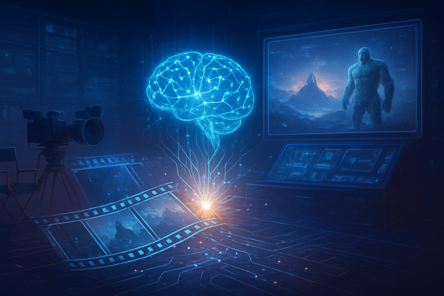
The Technical Canvas: From Prompts to Photorealism
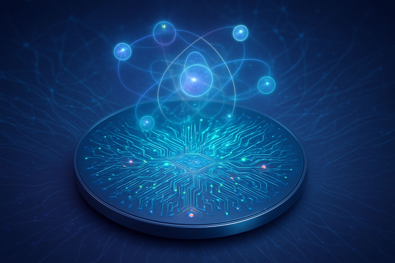
The core of this impending revolution lies in sophisticated Generative AI models that transcend traditional Computer-Generated Imagery (CGI) by moving beyond manual construction to automated creation from high-level prompts. Leading this charge are advancements in text-to-video and 3D world generation. OpenAI's (NASDAQ: MSFT) Sora, for instance, is a groundbreaking diffusion transformer capable of producing realistic and imaginative video scenes up to one minute in length from textual descriptions. Unlike previous models, Sora leverages a denoising latent diffusion model with a Transformer as its denoiser, generating videos in a latent space by denoising 3D "patches" and then converting them. It can even infer different camera angles without explicit prompts and has shown a surprising ability to generate 3D graphics from its training data, though it still grapples with perfect physical accuracy and intricate details like human hands.
Another significant player is Runway ML, which has iteratively developed its Gen-1, Gen-2, and Gen-4 models. Gen-2, notably, was among the first publicly available text-to-video models, capable of creating entirely new video content from text or stylizing existing footage. Recent updates have pushed its resolution, fidelity, and consistency, allowing for outputs exceeding Full HD. These tools differ fundamentally from traditional CGI, which requires meticulous, labor-intensive manual construction by artists for every detail—modeling, texturing, rigging, animation, lighting, and rendering. Generative AI shifts this paradigm from "creation by instruction" to "creation by prompt," automating rote tasks like rotoscoping and enabling rapid ideation and iteration, significantly reducing time and cost.
Beyond video, Generative AI is transforming 3D asset and world creation. Tools like World Labs' Marble model allow users to generate persistent 3D environments from a single image, enabling real-time navigation. Luma AI creates photorealistic 3D models from text and can convert live video into dynamic 3D environments, leveraging technologies such as Neural Radiance Fields (NeRFs) and 3D Gaussian Splatting for realistic scene synthesis. Companies like Autodesk (NASDAQ: ADSK) with Flow Studio (formerly Wonder Studio) offer cloud-based, AI-powered toolsets that convert live-action footage into editable CG scenes, reconstructing them in 3D space and matching camera and character movements. Even text-to-image generators like Midjourney, which employ diffusion-based models and Generative Adversarial Networks (GANs), serve as foundational tools, influencing visual style and prompt engineering for subsequent video and 3D workflows.
The AI research community, while acknowledging the immense potential for new artistic expressions, is actively addressing challenges like maintaining temporal and object consistency, achieving perfect physical accuracy, and improving fine-grained control over AI outputs. Concerns also loom over computational demands and the phenomenon of "hallucinations" where AI generates content misaligned with intent. Industry experts, including filmmakers and VFX artists, are excited by the efficiency gains and the potential to democratize high-quality effects. However, a strong undercurrent of apprehension exists regarding job displacement, creative control, and intellectual property. Prominent figures like James Cameron have expressed strong reservations, calling AI-generated performances "horrifying" and emphasizing the irreplaceable human element of emotional honesty, highlighting a critical debate on whether AI augments or replaces human artistry.
The Corporate Canvas: Giants, Innovators, and the New Gold Rush
The rise of Generative AI is creating a new competitive battleground, profoundly impacting tech giants, specialized AI companies, and nimble startups within the film and TV ecosystem. Foundational AI model developers like OpenAI (NASDAQ: MSFT) are poised to be major beneficiaries, licensing their cutting-edge technologies—such as the text-to-video model Sora—as the backbone for countless industry applications. Their strategic advantage lies in the development of highly capable and versatile models that can generate movie-quality effects and video clips from simple prompts, making them critical enablers for the entire creative workflow. However, the race for superior models is intense, with intellectual property rights and the provenance of training data emerging as significant concerns, as reports suggest widespread use of copyrighted material without explicit permission.
Tech giants are strategically leveraging their vast resources. Google (NASDAQ: GOOGL, NASDAQ: GOOG) is developing its own generative AI models like Lumiere for video and integrating its broader Gemini AI, while also investing heavily in custom AI chips (TPUs) to optimize performance and reduce reliance on external hardware. Similarly, Meta (NASDAQ: META) is focusing on AI for content moderation, recommendations, and metaverse development, simultaneously building its own AI chips (MTIA) to gain greater control and efficiency. Adobe (NASDAQ: ADBE) stands out by integrating its Firefly family of generative AI models directly into its ubiquitous Creative Cloud suite, offering "commercially safe" solutions trained on licensed content—a crucial differentiator that appeals strongly to professional creators wary of copyright infringement. This strategy aims to augment existing products and maintain market dominance rather than disrupt its user base.
Nvidia (NASDAQ: NVDA) remains an indispensable powerhouse, providing the GPUs that are the computational bedrock for training and deploying these complex generative AI models. Its NeMo language service and Picasso image, video, and 3D services further empower enterprises to build proprietary AI applications. However, Nvidia's dominance is attracting competition, with tech giants actively developing their own custom AI chips to reduce dependency. Microsoft (NASDAQ: MSFT), through its multi-billion dollar investment in OpenAI and its Azure AI services, is strategically integrating advanced generative AI across its cloud offerings, simultaneously developing its own AI accelerators (Azure Maia AI) to bolster its Azure cloud AI ecosystem. These moves indicate a broader trend among tech giants to internalize AI development and infrastructure, securing long-term strategic advantages.
Startups, characterized by their agility and specialization, are also carving out significant niches. Companies like RunwayML and Pika Labs are offering "best-in-class" text-to-video generation, disrupting traditional workflows by providing targeted solutions for tasks like AI-assisted storyboarding, visual effects, and automated dubbing (e.g., Flawless's TrueSync). Generative AI lowers the barrier to entry, enabling smaller companies and independent filmmakers to produce high-quality content more affordably, challenging the established order of major studios. These startups thrive by focusing on specific pain points, offering intuitive user interfaces, and demonstrating clear cost and time savings. The competitive landscape is thus a dynamic interplay between established giants leveraging their scale and infrastructure, and innovative startups pushing the boundaries of specific AI applications, all vying for a share in a rapidly evolving market.
The Wider Canvas: Societal Shifts and Ethical Crossroads
As of December 2025, Generative AI stands as a monumental leap in the broader AI landscape, moving beyond mere prediction and classification to actively producing novel content across text, image, video, and audio. This era of multimodal generative AI, exemplified by models like OpenAI's (NASDAQ: MSFT) Sora and Google's (NASDAQ: GOOGL, NASDAQ: GOOG) Gemini 1.5, signifies a shift from isolated tool experimentation to strategic, full-scale enterprise implementation. The trend is towards integrated AI platforms that can seamlessly operate across various data types, fostering autonomous AI assistants within creative workflows and driving ecosystem convergence. This profound evolution is not just a technological advancement but a societal inflection point, promising creative renewal and unprecedented efficiency while simultaneously raising fundamental questions about the nature of art, authenticity, and human labor.
The cultural impacts are two-fold. On one hand, Generative AI offers a democratic pathway to filmmaking, allowing independent creators with limited budgets to produce high-quality content that was once the exclusive domain of large studios. It facilitates hyper-personalized audience engagement, dynamic storylines, and localized content through advanced dubbing and translation, potentially transforming local narratives into global phenomena. On the other hand, deep-seated concerns persist regarding the erosion of human artistry and cultural authenticity. Critics like director James Cameron voice apprehension about AI generating characters and performances from scratch, arguing that AI, being trained on existing data, tends to produce an "average" of human experience rather than unique, individual creativity, thereby risking the "soul" of artistic expression.
The most pressing concerns revolve around job displacement, ethical dilemmas, and intellectual property. Projections indicate that over 20% of jobs in the US film, TV, and animation industry—amounting to over 200,000 positions—could be significantly disrupted by AI by 2026, particularly in visual effects, dubbing, editing, and animation. This threatens entry and mid-level roles, potentially limiting career development for aspiring talent. Ethically, the increasing realism of AI-generated video tools, like Sora, raises the specter of "industrial-scale misinformation pipelines" and "likeness theft," necessitating robust safeguards and transparency from studios to combat deepfakes and maintain public trust. The legal landscape for intellectual property remains murky; as of November 2025, court cases regarding the use of copyrighted material for AI training have yielded contradictory verdicts, and the U.S. Copyright Office maintains that purely AI-generated works, without sufficient human authorship, are not copyrightable.
This current wave of Generative AI represents a more fundamental shift than previous AI milestones. While AI has long supported production schedules or script analysis, generative AI actively participates in creating the content itself. Its disruptive potential is often compared to historical technological shifts, such as the impact of automation on manufacturing jobs in the 1980s, signaling a critical inflection point for creative industries. Unlike motion-capture technology, which enhances human performance, the ability of generative AI to create performances from scratch is viewed by some as a potentially dehumanizing force, highlighting a deep philosophical divide on the role of technology in art. The industry is currently grappling with defining the precise balance between AI augmentation and the irreplaceable essence of human creativity.
The Horizon: A Future Forged by Algorithms
As of December 2025, the film and TV industry stands at the precipice of even more profound changes driven by Generative AI. In the near term, we can expect AI to become an indispensable tool across all stages of production. Pre-production will see AI accelerating storyboarding, generating 3D models for sets, and optimizing camera paths, allowing directors to rapidly visualize and iterate on scenes with unprecedented speed and cost efficiency. Post-production will be further streamlined, with AI automating cosmetic improvements, de-aging actors, sophisticated dialogue replacement, and VFX microtasks, potentially achieving 80-90% efficiency gains in areas like shot extension and element removal. Furthermore, AI will evolve into a powerful scriptwriting collaborator, assisting with brainstorming, dialogue crafting, and plot structuring, significantly cutting down pre-production timelines.
Looking further ahead, towards 2030 and beyond, the industry anticipates truly transformative shifts. Experts, including Cristóbal Valenzuela, CEO of Runway, boldly predict the emergence of the first fully AI-generated feature films reaching major theaters as early as the end of 2025, democratizing film production and drastically reducing traditional budget requirements. The rise of multimodal AI models, capable of seamlessly processing and generating text, images, audio, and 3D content from a single prompt, will lead to highly integrated and efficient production pipelines. This will enable hyper-personalized and interactive entertainment experiences, where viewers can influence storylines or even insert themselves into narratives, moving beyond static content to dynamic, AI-curated entertainment journeys. The industry model itself is poised for a fundamental restructuring, with user-generated content powered by accessible AI tools becoming a significant part of mainstream TV.
However, this future is not without its hurdles. The primary challenges remain job displacement, particularly for VFX artists, animators, and entry-level roles, with estimates suggesting over 100,000 jobs in the U.S. sector could be "disrupted" by 2026. Intellectual property and copyright issues continue to be a legal battleground, with ongoing lawsuits challenging the use of copyrighted material for AI training and the copyrightability of AI-generated content. Ethical considerations, including bias in AI outputs, privacy concerns, and the preservation of human creativity, demand urgent attention. While AI is advancing rapidly, addressing the "uncanny valley" effect in photorealistic human depictions and generating longer, coherent narratives at a blockbuster quality level remain significant technical and creative challenges. Experts predict a future of "hybrid AI pipelines" blending AI-generated elements with traditional techniques, and a continued focus on specialized "creative co-pilots" to augment human artistry rather than replace it, alongside increased scrutiny on ethical and regulatory frameworks.
The Grand Finale: Reshaping the Art of Storytelling
As of December 2025, Generative AI has firmly established itself not as a fleeting trend, but as a foundational recalibrator of the film and television industry. The key takeaways are clear: AI is driving unprecedented operational efficiencies in backend tasks like contract management, marketing, and localization, significantly reducing costs and enhancing profitability for studios. It is revolutionizing pre- and post-production workflows, streamlining everything from script evaluation and storyboarding to complex VFX and editing. Crucially, Generative AI is democratizing content creation, empowering independent filmmakers with limited resources to produce high-quality content, fostering a "prompt-first filmmaking" approach that challenges traditional gatekeepers. While job displacement remains a significant concern, the prevailing sentiment leans towards AI augmenting human creativity, rather than outright replacing it, though the contentious issues of intellectual property and fair compensation for artists continue to evolve.
This development marks a pivotal moment in AI history, akin to the advent of streaming for the entertainment industry. Building on breakthroughs like Generative Adversarial Networks (GANs) in 2014 and the mainstream arrival of large language models like ChatGPT in late 2022, Generative AI has rapidly matured into a transformative tool capable of producing novel, sophisticated outputs. Its significance lies in its ability to fundamentally alter how content is conceived, produced, and consumed, pushing the boundaries of what's creatively and economically feasible. In the long term, Generative AI is poised to restructure the entire entertainment landscape, fostering hyper-personalized audience experiences and unlocking new storytelling formats, while simultaneously forcing a re-evaluation of the human element in art.
In the coming weeks and months, watch for accelerated studio experimentation with Generative AI in core content creation, particularly text-to-video, alongside continued rapid integration into operational functions for business optimization. Anticipate further advancements in image, audio, and video generation models, delivering even more realistic and controllable outputs. The legal battleground around intellectual property and fair use of training data will intensify, likely leading to more defined frameworks. New job roles, such as prompt engineers and AI ethicists, will continue to emerge, highlighting the evolving human-AI collaboration. The independent filmmaking community will remain a hotbed for innovation, pushing creative boundaries with accessible AI tools, while the industry as a whole grapples with preserving authenticity and the unique emotional resonance of human-created works in an increasingly AI-augmented world.
This content is intended for informational purposes only and represents analysis of current AI developments.
TokenRing AI delivers enterprise-grade solutions for multi-agent AI workflow orchestration, AI-powered development tools, and seamless remote collaboration platforms.
For more information, visit https://www.tokenring.ai/.