Government bodies worldwide are rapidly embracing Artificial Intelligence (AI) and data analytics, ushering in a transformative era aimed at enhancing public services, streamlining operations, and improving governance. This accelerating trend signals a significant shift towards data-driven decision-making, promising increased efficiency, cost savings, and more personalized citizen engagement. The adoption is driven by escalating demands from citizens for more efficient and responsive services, along with the need to manage vast amounts of public data that are too complex for manual analysis.
This paradigm shift is characterized by leveraging machine learning, predictive analytics, and automation to process vast amounts of data, extract meaningful insights, and anticipate future challenges with unprecedented speed and accuracy. Governments are strategically integrating AI into broader e-government and digital transformation initiatives, building on modernized IT systems and digitized processes. This involves fostering a data-driven mindset within organizations, establishing robust data governance practices, and developing frameworks to address ethical concerns, ensure accountability, and promote transparency in AI-driven decisions.
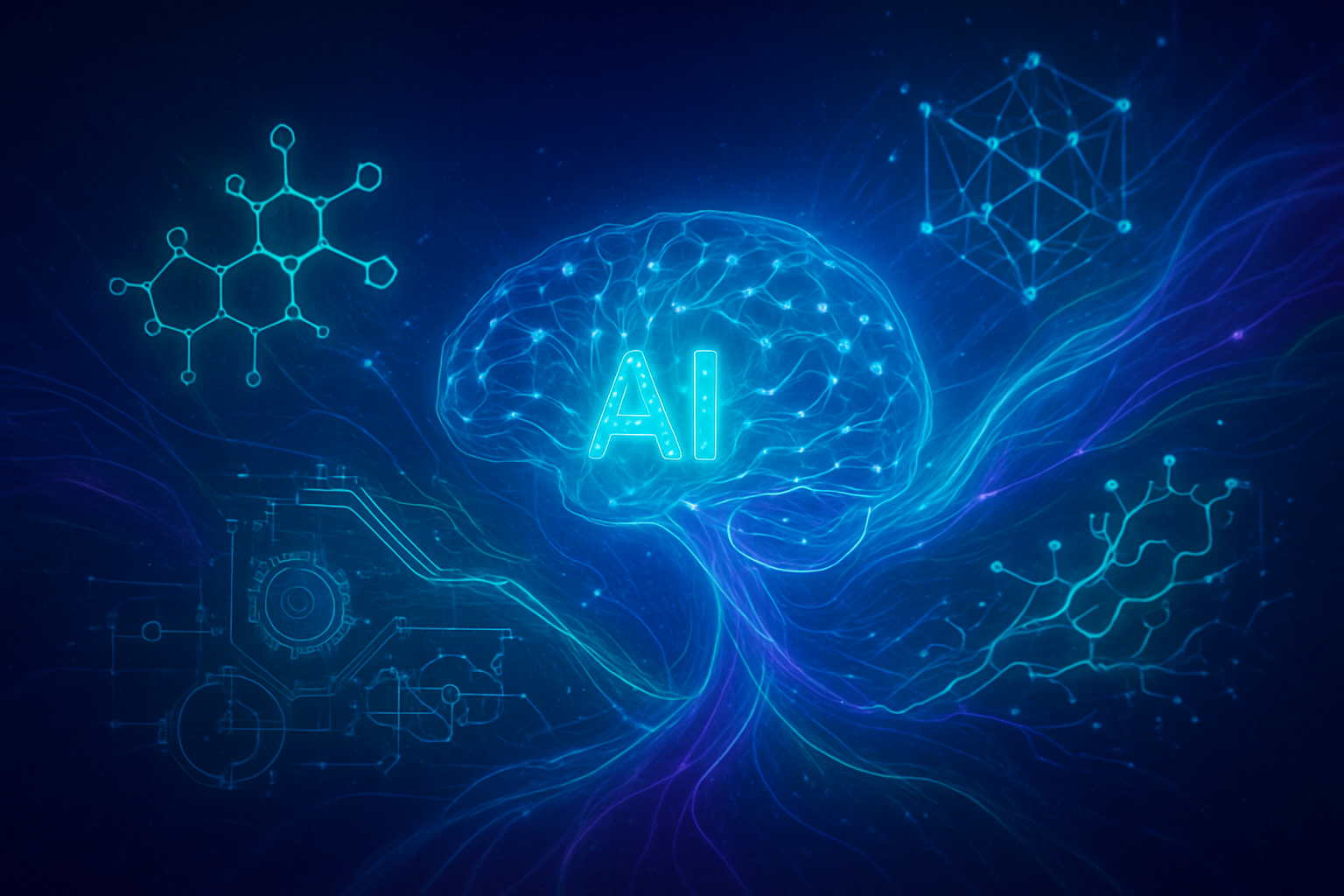
The Technical Core: AI Advancements Powering Public Sector Transformation
The current wave of government AI adoption is underpinned by sophisticated technical capabilities that significantly diverge from previous, often static, rule-based approaches. These advancements are enabling real-time analysis, predictive power, and adaptive learning, revolutionizing how public services are delivered.
Specific technical advancements and their applications include:
- Fraud Detection and Prevention: AI systems utilize advanced machine learning (ML) models and neural networks to analyze vast datasets of financial transactions and public records in real-time. These systems identify anomalous patterns and suspicious behaviors, adapting to evolving fraud schemes. For instance, the U.S. Treasury Department has employed ML since 2022, preventing or recovering over $4 billion in fiscal year 2024 by analyzing transaction data. This differs from older rule-based systems by continuously learning and improving accuracy, often by over 50%.
- Urban Planning and Smart Cities: AI in urban planning leverages geospatial analytics and predictive modeling from sensors and urban infrastructure. Capabilities include predicting traffic patterns, optimizing traffic flow, and managing critical infrastructure like power grids. Singapore, for example, uses AI for granular citizen services, such as collecting available badminton courts based on user preferences. Unlike slow, manual data collection, AI provides data-driven insights at unprecedented scale and speed for proactive development.
- Healthcare and Public Health: Federal health agencies are implementing AI for diagnostics, administrative efficiency, and predictive health analytics. AI models process medical imaging and electronic health records (EHRs) for faster disease detection (e.g., cancer), streamline clinical workflows (e.g., speech-to-text), and forecast disease outbreaks. The U.S. Department of Health and Human Services (HHS) has numerous AI use cases. This moves beyond static data analysis, offering real-time insights and personalized treatment plans.
- Enhanced Citizen Engagement and Services: Governments are deploying Natural Language Processing (NLP)-powered chatbots and virtual assistants that provide 24/7 access to information. These tools handle routine inquiries, assist with forms, and offer real-time information. Some government chatbots have handled over 3 million conversations, resolving 88% of queries on first contact. This offers instant, personalized interactions, a significant leap from traditional call centers.
- Defense and National Security: AI and ML are crucial for modern defense, enabling autonomous systems (drones, unmanned vehicles), predictive analytics for threat forecasting and equipment maintenance, and enhanced cybersecurity. The Defense Intelligence Agency (DIA) is actively seeking AI/ML prototype projects. AI significantly enhances the speed and accuracy of threat detection and response, reducing risks to human personnel in dangerous missions.
Initial reactions from the AI research community and industry experts are a mix of optimism and caution. While acknowledging AI's potential for enhanced efficiency, improved service delivery, and data-driven decision-making, paramount concerns revolve around data privacy, algorithmic bias, and the need for robust ethical and regulatory frameworks. Experts emphasize the importance of explainable AI (XAI) for transparency and accountability, especially given AI's direct impact on citizens. Skill gaps within government workforces and the quality of data used to train AI models are also highlighted as critical challenges.
Market Dynamics: AI Companies Vie for Government Contracts
The growing adoption of AI and data analytics by governments is creating a dynamic and lucrative market, projected to reach USD 135.7 billion by 2035. This shift significantly benefits a diverse range of companies, from established tech giants to agile startups and traditional government contractors.
Tech Giants like Amazon Web Services (AWS) (NASDAQ: AMZN), Google (NASDAQ: GOOGL), and Microsoft (NASDAQ: MSFT) are at the forefront, leveraging their extensive cloud infrastructure, advanced AI/ML capabilities, and robust security frameworks. Their strategic advantage lies in providing integrated "full-stack" solutions tailored for government needs, including compliance certifications and specialized government cloud regions. AWS, for example, recently announced an investment of up to $50 billion to expand its AI and supercomputing infrastructure for federal agencies, aiming to add nearly 1.3 gigawatts of computing capacity across its secure Top Secret, Secret, and GovCloud (US) regions. Google, along with OpenAI and Anthropic, recently received contracts worth up to $200 million from the U.S. Department of Defense (DoD) for advanced AI capabilities.
Specialized AI/Data Analytics Companies like Palantir Technologies (NYSE: PLTR) are titans in this space. Palantir's Gotham platform is critical for defense and intelligence agencies, while its Foundry platform serves commercial and civil government sectors. It has secured significant contracts, including a $795 million to $1.3 billion DoD deal for data fusion and AI programs, and a potential $10 billion Enterprise Service Agreement with the U.S. Army. NVIDIA (NASDAQ: NVDA), while not a direct government contractor for AI services, is foundational, as its GPU technology powers virtually all government AI initiatives.
AI Startups are gaining traction by focusing on niche innovations. Generative AI leaders like OpenAI, Anthropic, and xAI have received direct contracts from the Pentagon. OpenAI's ChatGPT Enterprise and Anthropic's Claude have been approved for government-wide use by the General Services Administration. Other specialized startups like CITYDATA.ai (local data insights for smart cities), CrowdAI (military intelligence processing), and Shield AI (software/hardware for autonomous military aircraft) are securing crucial early revenue.
Traditional Government Contractors and Integrators such as Booz Allen Hamilton (NYSE: BAH), ManTech (NASDAQ: MANT), and SAIC (NYSE: SAIC) are integrating AI into their existing service portfolios, enhancing offerings in defense, cybersecurity, and public services. Booz Allen Hamilton, a leader in scaling AI solutions for federal missions, has approximately $600 million in annual revenue from AI projects and aims to surpass $1 billion.
The competitive landscape is characterized by cloud dominance, where tech giants offer secure, government-accredited environments. Specialized firms like Palantir thrive on deep integration for complex government challenges, while startups drive innovation. Strategic partnerships and acquisitions are common, allowing faster integration of cutting-edge AI into government-ready solutions. Companies prioritizing "Responsible AI" and ethical frameworks are also gaining a competitive edge. This shift disrupts legacy software and manual processes through automation, enhances cybersecurity, and transforms government procurement by automating bid management and contract lifecycle.
Broader Significance: Reshaping Society and Governance
The adoption of AI and data analytics by governments marks a profound evolution in public administration, promising to redefine governance, enhance public services, and influence the broader technological landscape. This transformation brings both substantial opportunities and considerable challenges, echoing past technological revolutions in their profound impact on society and citizens.
In the broader AI landscape, government adoption is part of a global trend where AI is seen as a key driver of economic and social development across both private and public sectors. Many countries, including the UK, India, and the US, have developed national AI strategies to guide research and development, build human capacity, and establish regulatory frameworks. This indicates a move from isolated pilot projects to a more systematic and integrated deployment of AI across various government operations. The public sector is projected to be among the largest investors in AI by 2025, with a significant compound annual growth rate in investment.
For citizens, the positive impacts include enhanced service delivery and efficiency, with 24/7 accessibility through AI-powered assistants. AI enables data-driven decision-making, leading to more effective and impactful policies in areas like public safety, fraud detection, and personalized interactions. However, significant concerns loom large, particularly around privacy, as AI systems often rely on vast amounts of personal and sensitive data, raising fears of unchecked surveillance and data breaches. Ethical implications and algorithmic bias are critical, as AI systems can perpetuate existing societal biases if trained on unrepresentative data, leading to discrimination in areas like healthcare and law enforcement. Job displacement is another concern, though experts often highlight AI's role in augmenting human capabilities, necessitating significant investment in workforce reskilling. Transparency, accountability, and security risks associated with AI-driven technologies also demand robust governance.
Comparing this to previous technological milestones in governance, such as the introduction of computers and the internet, reveals parallels. Just as computers automated record-keeping and e-governance streamlined processes, AI now automates complex data analysis and personalizes service delivery. The internet facilitated data sharing; AI goes further by actively processing data to derive insights and predict outcomes in real-time. Each wave brought similar challenges related to infrastructure, workforce skills, and the need for new legal and ethical frameworks. AI introduces new complexities, particularly concerning algorithmic bias and the scale of data collection, demanding proactive and thoughtful strategic implementation.
The Horizon: Future Developments and Emerging Challenges
The integration of AI and data analytics is poised to profoundly transform government operations in the near and long term, leading to enhanced efficiency, improved service delivery, and more informed decision-making.
In the near term (1-5 years), governments are expected to significantly advance their use of AI through:
- Multimodal AI: Agencies will increasingly utilize AI that can understand and analyze information from various sources simultaneously (text, images, video, audio) for comprehensive data analysis in areas like climate risk assessment.
- AI Agents and Virtual Assistants: Sophisticated AI agents capable of reasoning and planning will emerge, handling complex tasks, managing applications, identifying security threats, and providing 24/7 citizen support.
- Assistive Search: Generative AI will transform how government employees access and understand information, improving the accuracy and efficiency of searching vast knowledge bases.
- Increased Automation: AI will automate mundane and process-heavy routines across government functions, freeing human employees for mission-critical tasks.
- Enhanced Predictive Analytics: Governments will increasingly leverage predictive analytics to forecast trends, optimize resource allocation, and anticipate public needs in areas like disaster preparedness and healthcare demand.
Long-term developments will see AI fundamentally reshaping the public sector, with a focus on augmentation over automation, where AI "copilots" enhance human capabilities. This will lead to a reimagining of public services and potentially a new industrial renaissance driven by AI and robotics. The maturity of AI governance and ethical standards, potentially grounded in legislation, will be crucial for responsible deployment.
Future applications include 24/7 virtual assistants for citizen services, AI-powered document automation for administrative tasks, enhanced cybersecurity and fraud detection, and predictive policy planning for climate change risks and urban development. In healthcare, AI will enable real-time disease monitoring, prediction, and hospital resource optimization.
However, several challenges must be addressed. Persistent issues with data quality, inconsistent formats, and data silos hinder effective AI implementation. A significant talent and skills gap exists within government agencies, requiring substantial investment in training. Many agencies rely on legacy infrastructure not designed for modern AI/ML. Ethical and governance concerns are paramount, including algorithmic bias, privacy infringements, lack of transparency, and accountability. Organizational and cultural resistance also slows adoption.
Experts predict AI will become a cornerstone of public sector operations by 2025, leading to an increased pace of life and efficiency. The trend is towards AI augmenting human intelligence, though it will have a significant, uneven effect on the workforce. The regulatory environment will become much more intricate, with a "thicket of AI law" emerging. Governments need to invest in AI leadership, workforce training, and continue to focus on ethical and responsible AI deployment.
A New Chapter in Governance: The AI-Powered Future
The rapid acceleration of AI and data analytics adoption by governments worldwide marks a pivotal moment in public administration and AI history. This is not merely an incremental technological upgrade but a fundamental shift in how public services are conceived, delivered, and governed. The key takeaway is a move towards a more data-driven, efficient, and responsive public sector, but one that is acutely aware of the complexities and ethical responsibilities involved.
This development signifies AI's maturation beyond research labs into critical societal infrastructure. Unlike previous "AI winters," the current era is characterized by widespread practical application, substantial investment, and a concerted effort to integrate AI across diverse public sector functions. Its long-term impact on society and governance is profound: reshaping public services to be more personalized and accessible, evolving decision-making processes towards data-driven policies, and transforming the labor market within the public sector. However, the success of this transformation hinges on navigating critical ethical and societal risks, including algorithmic bias, privacy infringements, and the potential for mass surveillance.
What to watch for in the coming weeks and months includes the rollout of more comprehensive AI governance frameworks, executive orders, and agency-specific policies outlining ethical guidelines, data privacy, and security standards. The increasing focus on multimodal AI and sophisticated AI agents will enable governments to handle more complex tasks. Continued investment in workforce training and skill development, along with efforts to modernize data infrastructure and break down silos, will be crucial. Expect ongoing international cooperation on AI safety and ethics, and a sustained focus on building public trust through transparency and accountability in AI applications. The journey of government AI adoption is a societal transformation that demands continuous evaluation, adaptation, and a human-centered approach to ensure AI serves the public good.
This content is intended for informational purposes only and represents analysis of current AI developments.
TokenRing AI delivers enterprise-grade solutions for multi-agent AI workflow orchestration, AI-powered development tools, and seamless remote collaboration platforms.
For more information, visit https://www.tokenring.ai/.