Tag: Technology News

  • Intel Reclaims Silicon Crown: 18A Process Hits High-Volume Production as ‘PowerVia’ Reshapes the AI Landscape

    Intel Reclaims Silicon Crown: 18A Process Hits High-Volume Production as ‘PowerVia’ Reshapes the AI Landscape

    As of January 27, 2026, the global semiconductor hierarchy has undergone its most significant shift in a decade. Intel Corporation (NASDAQ:INTC) has officially announced that its 18A (1.8nm-class) manufacturing node has reached high-volume manufacturing (HVM) status, signaling the successful completion of its "five nodes in four years" roadmap. This milestone is not just a technical victory for Intel; it marks the company’s return to the pinnacle of process leadership, a position it had ceded to competitors during the late 2010s.

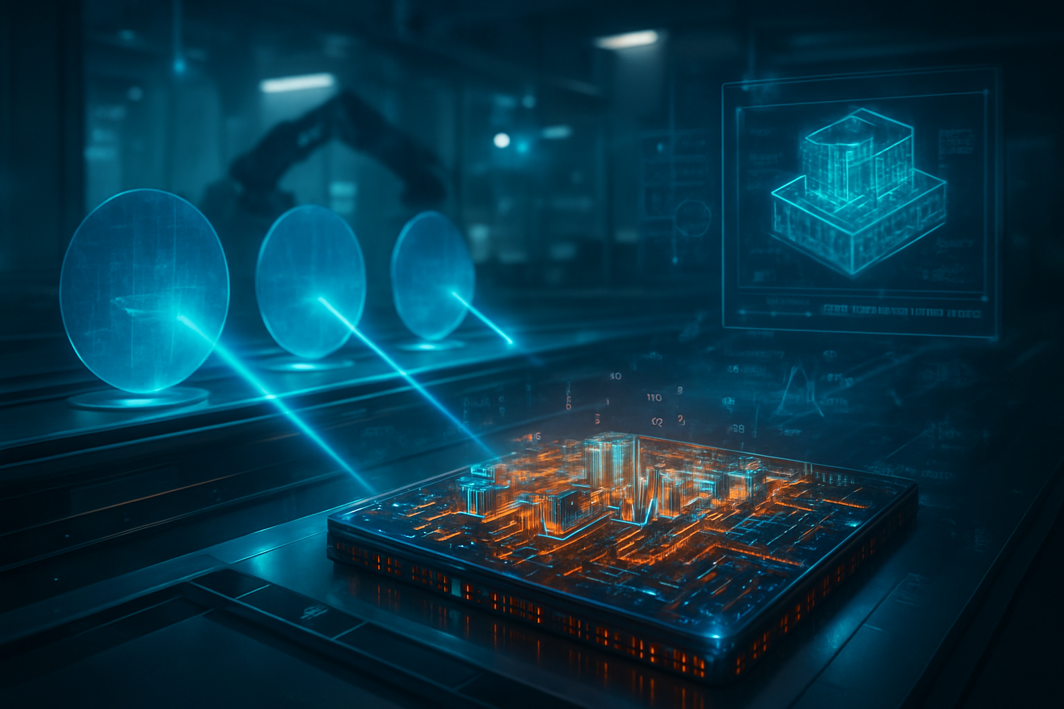
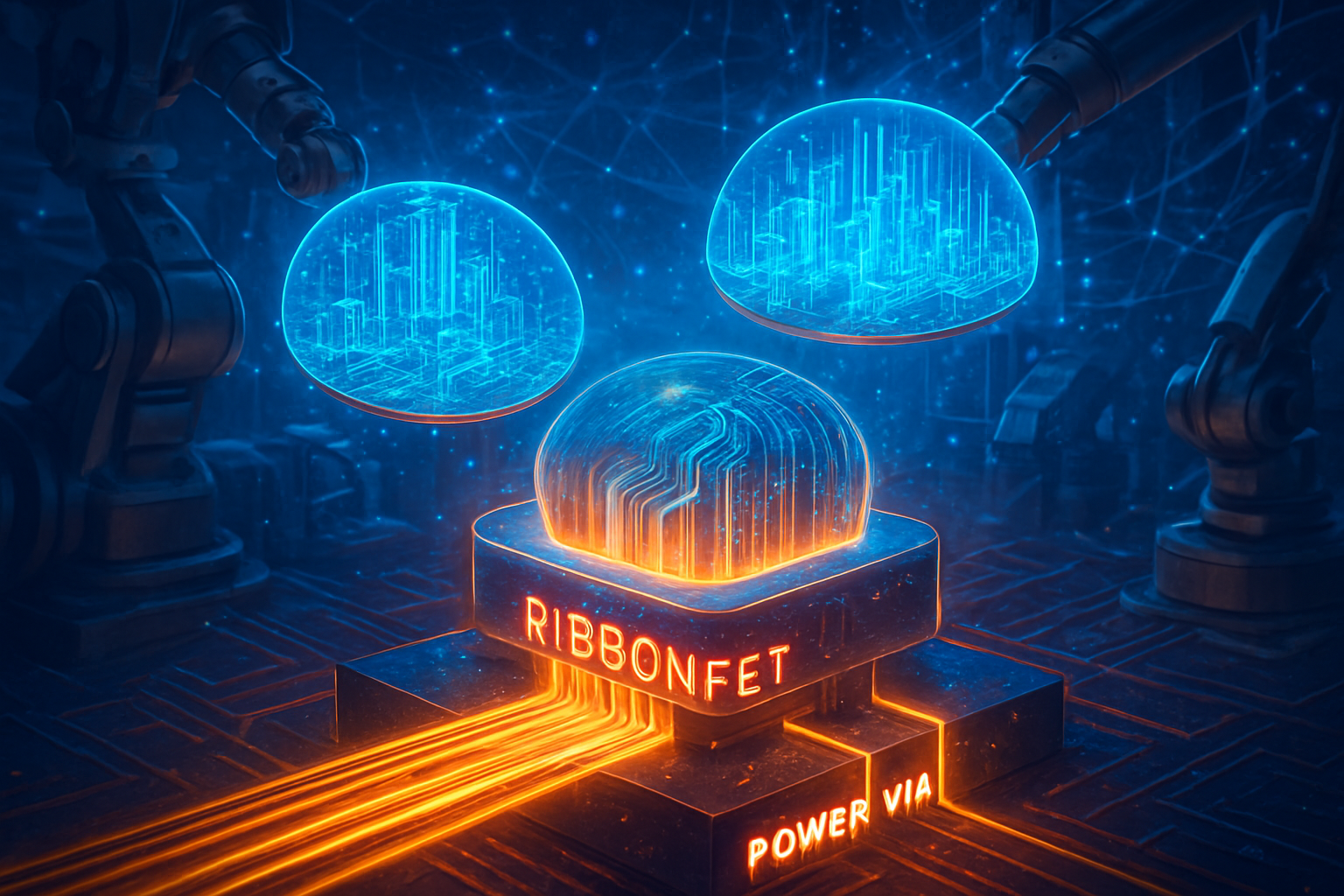
    The arrival of Intel 18A represents a critical turning point for the artificial intelligence industry. By integrating the revolutionary RibbonFET gate-all-around (GAA) architecture with its industry-leading PowerVia backside power delivery technology, Intel has delivered a platform optimized for the next generation of generative AI and high-performance computing (HPC). With early silicon already shipping to lead customers, the 18A node is proving to be the "holy grail" for AI developers seeking maximum performance-per-watt in an era of skyrocketing energy demands.

    The Architecture of Leadership: RibbonFET and the PowerVia Advantage

    At the heart of Intel 18A are two foundational innovations that differentiate it from the FinFET-based nodes of the past. The first is RibbonFET, Intel’s implementation of a Gate-All-Around (GAA) transistor. Unlike the previous FinFET design, which used a vertical fin to control current, RibbonFET surrounds the transistor channel on all four sides. This allows for superior control over electrical leakage and significantly faster switching speeds. The 18A node refines the initial RibbonFET design introduced in the 20A node, resulting in a 10-15% speed boost at the same power levels compared to the already impressive 20A projections.

    The second, and perhaps more consequential breakthrough, is PowerVia—Intel’s implementation of Backside Power Delivery (BSPDN). Traditionally, power and signal wires are bundled together on the "front" of the silicon wafer, leading to "routing congestion" and voltage droop. PowerVia moves the power delivery network to the backside of the wafer, using nano-TSVs (Through-Silicon Vias) to connect directly to the transistors. This decoupling of power and signal allows for much thicker, more efficient power traces, reducing resistance and reclaiming nearly 10% of previously wasted "dark silicon" area.

    While competitors like TSMC (NYSE:TSM) have announced their own version of this technology—marketed as "Superpower Rail" for their upcoming A16 node—Intel has successfully brought its version to market nearly a year ahead of the competition. This "first-mover" advantage in backside power delivery is a primary reason for the 18A node's high performance. Industry analysts have noted that the 18A node offers a 25% performance-per-watt improvement over the Intel 3 node, a leap that effectively resets the competitive clock for the foundry industry.

    Shifting the Foundry Balance: Microsoft, Apple, and the Race for AI Supremacy

    The successful ramp of 18A has sent shockwaves through the tech giant ecosystem. Intel Foundry has already secured a backlog exceeding $20 billion, with Microsoft (NASDAQ:MSFT) emerging as a flagship customer. Microsoft is utilizing the 18A-P (Performance-enhanced) variant to manufacture its next-generation "Maia 2" AI accelerators. By leveraging Intel's domestic manufacturing capabilities in Arizona and Ohio, Microsoft is not only gaining a performance edge but also securing its supply chain against geopolitical volatility in East Asia.

    The competitive implications extend to the highest levels of the consumer electronics market. Reports from late 2025 indicate that Apple (NASDAQ:AAPL) has moved a portion of its silicon production for entry-level devices to Intel’s 18A-P node. This marks a historic diversification for Apple, which has historically relied almost exclusively on TSMC for its A-series and M-series chips. For Intel, winning an "Apple-sized" contract validates the maturity of its 18A process and proves it can meet the stringent yield and quality requirements of the world’s most demanding hardware company.

    For AI hardware startups and established giants like NVIDIA (NASDAQ:NVDA), the availability of 18A provides a vital alternative in a supply-constrained market. While NVIDIA remains a primary partner for TSMC, the introduction of Intel’s 18A-PT—a variant optimized for advanced multi-die "System-on-Chip" (SoC) designs—offers a compelling path for future Blackwell successors. The ability to stack high-performance 18A logic tiles using Intel’s Foveros Direct 3D packaging technology is becoming a key differentiator in the race to build the first 100-trillion parameter AI models.

    Geopolitics and the Reshoring of the Silicon Frontier

    Beyond the technical specifications, Intel 18A is a cornerstone of the broader geopolitical effort to reshore semiconductor manufacturing to the United States. Supported by funding from the CHIPS and Science Act, Intel’s expansion of Fab 52 in Arizona has become a symbol of American industrial renewal. The 18A node is the first advanced process in over a decade to be pioneered and mass-produced on U.S. soil before any other region, a fact that has significant implications for national security and technological sovereignty.

    The success of 18A also serves as a validation of the "Five Nodes in Four Years" strategy championed by Intel’s leadership. By maintaining an aggressive cadence, Intel has leapfrogged the standard industry cycle, forcing competitors to accelerate their own roadmaps. This rapid iteration has been essential for the AI landscape, where the demand for compute is doubling every few months. Without the efficiency gains provided by technologies like PowerVia and RibbonFET, the energy costs of maintaining massive AI data centers would likely become unsustainable.

    However, the transition has not been without concerns. The immense capital expenditure required to maintain this pace has pressured Intel’s margins, and the complexity of 18A manufacturing requires a highly specialized workforce. Critics initially doubted Intel's ability to achieve commercial yields (currently estimated at a healthy 65-75%), but the successful launch of the "Panther Lake" consumer CPUs and "Clearwater Forest" Xeon processors has largely silenced the skeptics.

    The Road to 14A and the Era of High-NA EUV

    Looking ahead, the 18A node is just the beginning of Intel’s "Angstrom-era" roadmap. The company has already begun sampling its next-generation 14A node, which will be the first in the industry to utilize High-Numerical Aperture (High-NA) Extreme Ultraviolet (EUV) lithography tools from ASML (NASDAQ:ASML). While 18A solidified Intel's recovery, 14A is intended to extend that lead, targeting another 15% performance improvement and a further reduction in feature sizes.

    The integration of 18A technology into the "Nova Lake" architecture—scheduled for late 2026—will be the next major milestone for the consumer market. Experts predict that Nova Lake will redefine the desktop and mobile computing experience by offering over 50 TOPS of NPU (Neural Processing Unit) performance, effectively making every 18A-powered PC a localized AI powerhouse. The challenge for Intel will be maintaining this momentum while simultaneously scaling its foundry services to accommodate a diverse range of third-party designs.

    A New Chapter for the Semiconductor Industry

    The high-volume manufacturing of Intel 18A marks one of the most remarkable corporate turnarounds in recent history. By delivering 10-15% speed gains and pioneering backside power delivery via PowerVia, Intel has not only caught up to the leading edge but has actively set the pace for the rest of the decade. This development ensures that the AI revolution will have the "silicon fuel" it needs to continue its exponential growth.

    As we move further into 2026, the industry's eyes will be on the retail performance of the first 18A devices and the continued expansion of Intel Foundry's customer list. The "Angstrom Race" is far from over, but with 18A now in production, Intel has firmly re-established itself as a titan of the silicon world. For the first time in a generation, the fastest and most efficient transistors on the planet are being made by the company that started it all.


    This content is intended for informational purposes only and represents analysis of current AI developments.

    TokenRing AI delivers enterprise-grade solutions for multi-agent AI workflow orchestration, AI-powered development tools, and seamless remote collaboration platforms.
    For more information, visit https://www.tokenring.ai/.
  • The Silicon Shield Moves West: US and Taiwan Ink $500 Billion AI and Semiconductor Reshoring Pact

    The Silicon Shield Moves West: US and Taiwan Ink $500 Billion AI and Semiconductor Reshoring Pact

    In a move that signals a seismic shift in the global technology landscape, the United States and Taiwan finalized a historic trade and investment agreement on January 15, 2026. The deal, spearheaded by the U.S. Department of Commerce, centers on a massive $250 billion direct investment pledge from Taiwanese industry titans to build advanced semiconductor and artificial intelligence production capacity on American soil. Combined with an additional $250 billion in credit guarantees from the Taiwanese government to support supply-chain migration, the $500 billion package represents the most significant effort in history to reshore the foundations of the digital age.

    The agreement aims to fundamentally alter the geographical concentration of high-end computing. Its central strategic pillar is an ambitious goal to relocate 40% of Taiwan’s entire chip supply chain to the United States within the next few years. By creating a domestic "Silicon Shield," the U.S. hopes to secure its leadership in the AI revolution while mitigating the risks of regional instability in the Pacific. For Taiwan, the pact serves as a "force multiplier," ensuring that its "Sacred Mountain" of tech companies remains indispensable to the global economy through a permanent and integrated presence in the American industrial heartland.

    The "Carrot and Stick" Framework: Section 232 and the Quota System

    The technical core of the agreement revolves around a sophisticated utilization of Section 232 of the Trade Expansion Act, transforming traditional protectionist tariffs into powerful incentives for industrial relocation. To facilitate the massive capital flight required, the U.S. has introduced a "quota-based exemption" model. Under this framework, Taiwanese firms that commit to building new U.S.-based capacity are granted the right to import up to 2.5 times their planned U.S. production volume from their home facilities in Taiwan entirely duty-free during the construction phase. Once these facilities become operational, the companies maintain a 1.5-times duty-free import quota based on their actual U.S. output.

    This mechanism is designed to prevent supply chain disruptions while the new American "Gigafabs" are being built. Furthermore, the agreement caps general reciprocal tariffs on a wide range of goods—including auto parts and timber—at 15%, down from previous rates that reached as high as 32% for certain sectors. For the AI research community, the inclusion of 0% tariffs on generic pharmaceuticals and specialized aircraft components is seen as a secondary but vital win for the broader high-tech ecosystem. Initial reactions from industry experts have been largely positive, with many praising the deal's pragmatic approach to bridging the cost gap between manufacturing in East Asia versus the United States.

    Corporate Titans Lead the Charge: TSMC, Foxconn, and the 2nm Race

    The success of the deal rests on the shoulders of Taiwan’s largest corporations. Taiwan Semiconductor Manufacturing Co., Ltd. (NYSE: TSM) has already confirmed that its 2026 capital expenditure will surge to a record $52 billion to $56 billion. As a direct result of the pact, TSM has acquired hundreds of additional acres in Arizona to create a "Gigafab" cluster. This expansion is not merely about volume; it includes the rapid deployment of 2nm production lines and advanced "CoWoS" packaging facilities, which are essential for the next generation of AI accelerators used by firms like NVIDIA Corp. (NASDAQ: NVDA).

    Hon Hai Precision Industry Co., Ltd., better known as Foxconn (OTC: HNHPF), is also pivoting its U.S. strategy toward high-end AI infrastructure. Under the new trade framework, Foxconn is expanding its footprint to assemble the highly complex NVL 72 AI servers for NVIDIA and has entered a strategic partnership with OpenAI to co-design AI hardware components within the U.S. Meanwhile, MediaTek Inc. (TPE: 2454) is shifting its smartphone System-on-Chip (SoC) roadmap to utilize U.S.-based 2nm nodes, a strategic move to avoid potential 100% tariffs on foreign-made chips that could be applied to companies not participating in the reshoring initiative. This positioning grants these firms a massive competitive advantage, securing their access to the American market while stabilizing their supply lines against geopolitical volatility.

    A New Era of Economic Security and Geopolitical Friction

    This agreement is more than a trade deal; it is a declaration of economic sovereignty. By aiming to bring 40% of the supply chain to the U.S., the Department of Commerce is attempting to reverse a thirty-year decline in American wafer fabrication, which fell from a 37% global share in 1990 to less than 10% in 2024. The deal seeks to replicate Taiwan’s successful "Science Park" model in states like Arizona, Ohio, and Texas, creating self-sustaining industrial clusters where R&D and manufacturing exist side-by-side. This move is seen as the ultimate insurance policy for the AI era, ensuring that the hardware required for LLMs and autonomous systems is produced within a secure domestic perimeter.

    However, the pact has not been without its detractors. Beijing has officially denounced the agreement as "economic plunder," accusing the U.S. of hollowing out Taiwan’s industrial base for its own gain. Within Taiwan, a heated debate persists regarding the "brain drain" of top engineering talent to the U.S. and the potential loss of the island's "Silicon Shield"—the theory that its dominance in chipmaking protects it from invasion. In response, Taiwanese Vice Premier Cheng Li-chiun has argued that the deal represents a "multiplication" of Taiwan's strength, moving from a single island fortress to a global distributed network that is even harder to disrupt.

    The Road Ahead: 2026 and Beyond

    Looking toward the near-term, the focus will shift from diplomatic signatures to industrial execution. Over the next 18 to 24 months, the tech industry will watch for the first "breaking of ground" on the new Gigafab sites. The primary challenge remains the development of a skilled workforce; the agreement includes provisions for "educational exchange corridors," but the sheer scale of the 40% reshoring goal will require tens of thousands of specialized engineers that the U.S. does not currently have in reserve.

    Experts predict that if the "2.5x/1.5x" quota system proves successful, it could serve as a blueprint for similar trade agreements with other key allies, such as Japan and South Korea. We may also see the emergence of "sovereign AI clouds"—compute clusters owned and operated within the U.S. using exclusively domestic-made chips—which would have profound implications for government and military AI applications. The long-term vision is a world where the hardware for artificial intelligence is no longer a bottleneck or a geopolitical flashpoint, but a commodity produced with American energy and labor.

    Final Reflections on a Landmark Moment

    The US-Taiwan Agreement of January 2026 marks a definitive turning point in the history of the information age. By successfully incentivizing a $250 billion private sector investment and securing a $500 billion total support package, the U.S. has effectively hit the "reset" button on global manufacturing. This is not merely an act of protectionism, but a massive strategic bet on the future of AI and the necessity of a resilient, domestic supply chain for the technologies that will define the rest of the century.

    As we move forward, the key metrics of success will be the speed of fab construction and the ability of the U.S. to integrate these Taiwanese giants into its domestic economy without stifling innovation. For now, the message to the world is clear: the era of hyper-globalized, high-risk supply chains is ending, and the era of the "domesticated" AI stack has begun. Investors and industry watchers should keep a close eye on the quarterly Capex reports of TSMC and Foxconn throughout 2026, as these will be the first true indicators of how quickly this historic transition is taking hold.


    This content is intended for informational purposes only and represents analysis of current AI developments.

    TokenRing AI delivers enterprise-grade solutions for multi-agent AI workflow orchestration, AI-powered development tools, and seamless remote collaboration platforms.
    For more information, visit https://www.tokenring.ai/.

  • India’s Silicon Revolution: Groundbreaking for Dholera Fab Marks Bold Leap Toward 2032 Semiconductor Leadership

    India’s Silicon Revolution: Groundbreaking for Dholera Fab Marks Bold Leap Toward 2032 Semiconductor Leadership

    The landscape of global electronics manufacturing shifted significantly this week as India officially commenced the next phase of its ambitious semiconductor journey. The groundbreaking for the country’s first commercial semiconductor fabrication facility (fab) in the Dholera Special Investment Region (SIR) of Gujarat represents more than just a construction project; it is the physical manifestation of India’s intent to become a premier global tech hub. Spearheaded by a strategic partnership between Tata Electronics and Taiwan’s Powerchip Semiconductor Manufacturing Corp. (TWSE: 6770), the $11 billion (₹91,000 crore) facility is the cornerstone of the India Semiconductor Mission (ISM), aiming to insulate the nation from global supply chain shocks while fueling domestic high-tech growth.

    This milestone comes at a critical juncture as the Indian government doubles down on its long-term vision. Union ministers have reaffirmed a target for India to rank among the top four semiconductor nations globally by 2032, with an even more aggressive goal to lead the world in specific semiconductor verticals by 2035. For a nation that has historically excelled in chip design but lagged in physical manufacturing, the Dholera fab serves as the "anchor tenant" for a massive "Semicon City" ecosystem, signaling to the world that India is no longer just a consumer of technology, but a primary architect and manufacturer of it.

    Technical Specifications and Industry Impact

    The Dholera fab is engineered to be a high-volume, state-of-the-art facility capable of producing 50,000 12-inch wafers per month at full capacity. Technically, the facility is focusing its initial efforts on the 28-nanometer (nm) technology node. While advanced logic chips for smartphones often utilize smaller nodes like 3nm or 5nm, the 28nm node remains the "sweet spot" for a vast array of high-demand applications. These include Power Management Integrated Circuits (PMICs), display drivers, and microcontrollers essential for the automotive and industrial sectors. The facility is also designed with the flexibility to support mature nodes ranging from 40nm to 110nm, ensuring a wide-reaching impact on the electronics ecosystem.

    Initial reactions from the global semiconductor research community have been overwhelmingly positive, particularly regarding the partnership with PSMC. By leveraging the Taiwanese firm’s deep expertise in logic and memory manufacturing, Tata Electronics is bypassing decades of trial-and-error. Technical experts have noted that the "AI-integrated" infrastructure of the fab—which includes advanced automation and real-time data analytics for yield optimization—differentiates this project from traditional fabs in the region. The recent arrival of specialized lithography and etching equipment from Tokyo Electron (TYO: 8035) and other global leaders underscores the facility's readiness to meet international precision standards.

    Strategic Advantages for Tech Giants and Startups

    The establishment of this fab creates a seismic shift for major players across the tech spectrum. The primary beneficiary within the domestic market is the Tata Group, which can now integrate its own chips into products from Tata Motors Limited (NSE: TATAMOTORS) and its aerospace ventures. This vertical integration provides a massive strategic advantage in cost control and supply security. Furthermore, global tech giants like Micron Technology (NASDAQ: MU), which is already operating an assembly and test plant in nearby Sanand, now have a domestic wafer source, potentially reducing the lead times and logistics costs that have historically plagued the Indian electronics market.

    Competitive implications are also emerging for major AI labs and hardware companies. As the Dholera fab scales, it will likely disrupt the existing dominance of East Asian manufacturing hubs. By offering a "China Plus One" alternative, India is positioning itself as a reliable secondary source for global giants like Apple and NVIDIA (NASDAQ: NVDA), who are increasingly looking to diversify their manufacturing footprints. Startups in India’s burgeoning EV and IoT sectors are also expected to see a surge in innovation, as they gain access to localized prototyping and a more responsive supply chain that was previously tethered to overseas lead times.

    Broader Significance in the Global Landscape

    Beyond the immediate commercial impact, the Dholera project carries profound geopolitical weight. In the broader AI and technology landscape, semiconductors have become the new "oil," and India’s entry into the fab space is a calculated move to secure technological sovereignty. This development mirrors the significant historical milestones of the 1980s when Taiwan and South Korea first entered the market; if successful, India’s 2032 goal would mark one of the fastest ascents of a nation into the semiconductor elite in history.

    However, the path is not without its hurdles. Concerns have been raised regarding the massive requirements for ultrapure water and stable high-voltage power, though the Gujarat government has fast-tracked a dedicated 1.5-gigawatt power grid and specialized water treatment facilities to address these needs. Comparisons to previous failed attempts at Indian semiconductor manufacturing are inevitable, but the difference today lies in the unprecedented level of government subsidies—covering up to 50% of project costs—and the deep involvement of established industrial conglomerates like Tata Steel Limited (NSE: TATASTEEL) to provide the foundational infrastructure.

    Future Horizons and Challenges

    Looking ahead, the roadmap for India’s semiconductor mission is both rapid and expansive. Following the stabilization of the 28nm node, the Tata-PSMC joint venture has already hinted at plans to transition to 22nm and eventually explore smaller logic nodes by the turn of the decade. Experts predict that as the Dholera ecosystem matures, it will attract a cluster of "OSAT" (Outsourced Semiconductor Assembly and Test) and ATMP (Assembly, Testing, Marking, and Packaging) facilities, creating a fully integrated value chain on Indian soil.

    The near-term focus will be on "tool-in" milestones and pilot production runs, which are expected to commence by late 2026. One of the most significant challenges on the horizon will be talent cultivation; to meet the goal of being a top-four nation, India must train hundreds of thousands of specialized engineers. Programs like the "Chips to Startup" (C2S) initiative are already underway to ensure that by the time the Dholera fab reaches peak capacity, there is a workforce ready to operate and innovate within its walls.

    A New Era for Indian Silicon

    In summary, the groundbreaking at Dholera is a watershed moment for the Indian economy and the global technology supply chain. By partnering with PSMC and committing billions in capital, India is transitioning from a service-oriented economy to a high-tech manufacturing powerhouse. The key takeaways are clear: the nation has a viable path to 28nm production, a massive captive market through the Tata ecosystem, and a clear, state-backed mandate to dominate the global semiconductor stage by 2032.

    As we move through 2026, all eyes will be on the construction speed and the integration of supply chain partners like Applied Materials (NASDAQ: AMAT) and Lam Research (NASDAQ: LRCX) into the Dholera SIR. The success of this fab will not just be measured in wafers produced, but in the shift of the global technological balance of power. For the first time, "Made in India" chips are no longer a dream of the future, but a looming reality for the global market.


    This content is intended for informational purposes only and represents analysis of current AI and semiconductor developments.

    TokenRing AI delivers enterprise-grade solutions for multi-agent AI workflow orchestration, AI-powered development tools, and seamless remote collaboration platforms.
    For more information, visit https://www.tokenring.ai/.
  • The End of the Search Bar: OpenAI’s ‘Operator’ and the Dawn of the Action-Oriented Web

    The End of the Search Bar: OpenAI’s ‘Operator’ and the Dawn of the Action-Oriented Web

    Since the debut of ChatGPT, the world has viewed artificial intelligence primarily as a conversationalist—a digital librarian capable of synthesizing vast amounts of information into a coherent chat window. However, the release and subsequent integration of OpenAI’s "Operator" (now officially known as "Agent Mode") has shattered that paradigm. By moving beyond text generation and into direct browser manipulation, OpenAI has signaled the official transition from "Chat AI" to "Agentic AI," where the primary value is no longer what the AI can tell you, but what it can do for you.

    As of January 2026, Agent Mode has become a cornerstone of the ChatGPT ecosystem, fundamentally altering how millions of users interact with the internet. Rather than navigating a maze of tabs, filters, and checkout screens, users now delegate entire workflows—from booking multi-city international travel to managing complex retail returns—to an agent that "sees" and interacts with the web exactly like a human would. This development marks a pivotal moment in tech history, effectively turning the web browser into an operating system for autonomous digital workers.

    The Technical Leap: From Pixels to Performance

    At the heart of Operator is OpenAI’s Computer-Using Agent (CUA) model, a multimodal powerhouse that represents a significant departure from traditional web-scraping or API-based automation. Unlike previous iterations of "browsing" tools that relied on reading simplified text versions of a website, Operator operates within a managed virtual browser environment. It utilizes advanced vision-based perception to interpret the layout of a page, identifying buttons, text fields, and dropdown menus by analyzing the raw pixels of the screen. This allows it to navigate even the most modern, Javascript-heavy websites that typically break standard automation scripts.

    The technical sophistication of Operator is best demonstrated in its "human-like" interaction patterns. It doesn't just jump to a URL; it scrolls through pages to find information, handles pop-ups, and can even self-correct when a website’s layout changes unexpectedly. In benchmark tests conducted throughout 2025, OpenAI reported that the agent achieved an 87% success rate on the WebVoyager benchmark, a standard for complex browser tasks. This is a massive leap over the 30-40% success rates seen in early 2024 models. This leap is attributed to a combination of reinforcement learning and a "Thinking" architecture that allows the agent to pause and reason through a task before executing a click.

    Industry experts have been particularly impressed by the agent's "Human-in-the-Loop" safety architecture. To mitigate the risks of unauthorized transactions or data breaches, OpenAI implemented a "Takeover Mode." When the agent encounters a sensitive field—such as a credit card entry or a login screen—it automatically pauses and hands control back to the user. This hybrid approach has allowed OpenAI to navigate the murky waters of security and trust, providing a "Watch Mode" for high-stakes interactions where users can monitor every click in real-time.

    The Battle for the Agentic Desktop

    The emergence of Operator has ignited a fierce strategic rivalry among tech giants, most notably between OpenAI and its primary benefactor, Microsoft (NASDAQ: MSFT). While the two remain deeply linked through Azure's infrastructure, they are increasingly competing for the "agentic" crown. Microsoft has positioned its Copilot agents as structured, enterprise-grade tools built within the guardrails of Microsoft 365. While OpenAI’s Operator is a "generalist" that thrives in the messy, open web, Microsoft’s agents are designed for precision within corporate data silos—handling HR requests, IT tickets, and supply chain logistics with a focus on data governance.

    This "coopetition" is forcing a reorganization of the broader tech landscape. Google (NASDAQ: GOOGL) has responded with "Project Jarvis" (part of the Gemini ecosystem), which offers deep integration with the Chrome browser and Android OS, aiming for a "zero-latency" experience that rivals OpenAI's standalone virtual environment. Meanwhile, Anthropic has focused its "Computer Use" capabilities on developers and technical power users, prioritizing full OS control over the consumer-friendly browser focus of OpenAI.

    The impact on consumer-facing platforms has been equally transformative. Companies like Expedia (NASDAQ: EXPE) and Booking.com (NASDAQ: BKNG) were initially feared to be at risk of "disintermediation" by AI agents. However, by 2026, these companies have largely pivoted to become the essential back-end infrastructure for agents. Both Expedia and Booking.com have integrated deeply with OpenAI's agent protocols, ensuring that when an agent searches for a hotel, it is pulling from their verified inventories. This has shifted the battleground from SEO (Search Engine Optimization) to "AEO" (Agent Engine Optimization), where companies pay to be the preferred choice of the autonomous digital shopper.

    A Broader Shift: The End of the "Click-Heavy" Web

    The wider significance of Operator lies in its potential to render the traditional web interface obsolete. For decades, the internet has been designed for human eyes and fingers—designed to be "sticky" and encourage clicks to drive ad revenue. Agentic AI flips this model on its head. If an agent is doing the "clicking," the visual layout of a website becomes secondary to its functional utility. This poses a fundamental threat to the ad-supported "attention economy." If a user never sees a banner ad because their agent handled the transaction in a background tab, the primary revenue model for much of the internet begins to crumble.

    This transition has not been without its concerns. Privacy advocates have raised alarms about the "agentic risk" associated with giving AI models the ability to act on a user's behalf. In early 2025, several high-profile incidents involving "hallucinated transactions"—where an agent booked a non-refundable flight to the wrong city—highlighted the dangers of over-reliance. Furthermore, the ethical implications of agents being used to bypass CAPTCHAs or automate social media interactions have forced platforms like Amazon (NASDAQ: AMZN) and Meta (NASDAQ: META) to deploy "anti-agent" shields, creating a digital arms race between autonomous tools and the platforms they inhabit.

    Despite these hurdles, the consensus among AI researchers is that Operator represents the most significant milestone since the release of GPT-4. It marks the moment AI stopped being a passive advisor and became an active participant in the economy. This shift mirrors the transition from the mainframe era to the personal computer era; just as the PC put computing power in the hands of individuals, the agentic era is putting "doing power" in the hands of anyone with a ChatGPT subscription.

    The Road to Full Autonomy

    Looking ahead, the next 12 to 18 months are expected to focus on the evolution from browser-based agents to full "cross-platform" autonomy. Researchers predict that by late 2026, agents will not be confined to a virtual browser window but will have the ability to move seamlessly between desktop applications, mobile apps, and web services. Imagine an agent that can take a brief from a Zoom (NASDAQ: ZM) meeting, draft a proposal in Microsoft Word, research competitors in a browser, and then send a final invoice via QuickBooks without a single human click.

    The primary challenge remains "long-horizon reasoning." While Operator can book a flight today, it still struggles with tasks that require weeks of context or multiple "check-ins" (e.g., "Plan a wedding and manage the RSVPs over the next six months"). Addressing this will require a new generation of models capable of persistent memory and proactive notification—agents that don't just wait for a prompt but "wake up" to check on the status of a task and report back to the user.

    Furthermore, we are likely to see the rise of "Multi-Agent Systems," where a user's personal agent coordinates with a travel agent, a banking agent, and a retail agent to settle complex disputes or coordinate large-scale events. The "Agent Protocol" standard, currently under discussion by major tech firms, aims to create a universal language for these digital workers to communicate, potentially leading to a fully automated service economy.

    A New Era of Digital Labor

    OpenAI’s Operator has done more than just automate a few clicks; it has redefined the relationship between humans and computers. We are moving toward a future where "interacting with a computer" no longer means learning how to navigate software, but rather learning how to delegate intent. The success of this development suggests that the most valuable skill in the coming decade will not be technical proficiency, but the ability to manage and orchestrate a fleet of AI agents.

    As we move through 2026, the industry will be watching closely for how these agents handle increasingly complex financial and legal tasks. The regulatory response—particularly in the EU, where Agent Mode faced initial delays—will determine how quickly this technology becomes a global standard. For now, the "Action Era" is officially here, and the web as we know it—a place of links, tabs, and manual labor—is slowly fading into the background of an automated world.


    This content is intended for informational purposes only and represents analysis of current AI developments.

    TokenRing AI delivers enterprise-grade solutions for multi-agent AI workflow orchestration, AI-powered development tools, and seamless remote collaboration platforms.
    For more information, visit https://www.tokenring.ai/.
  • The Custom Silicon Arms Race: How Tech Giants are Reimagining the Future of AI Hardware

    The Custom Silicon Arms Race: How Tech Giants are Reimagining the Future of AI Hardware

    The landscape of artificial intelligence is undergoing a seismic shift. For years, the industry’s hunger for compute power was satisfied almost exclusively by off-the-shelf hardware, with NVIDIA (NASDAQ: NVDA) reigning supreme as the primary architect of the AI revolution. However, as the demands of large language models (LLMs) grow and the cost of scaling reaches astronomical levels, a new era has dawned: the era of Custom Silicon.

    In a move that underscores the high stakes of this technological rivalry, ByteDance has recently made headlines with a massive $14 billion investment in NVIDIA hardware. Yet, even as they spend billions on third-party chips, the world’s tech titans—Microsoft, Google, and Amazon—are racing to develop their own proprietary processors. This is no longer just a competition for software supremacy; it is a race to own the very "brains" of the digital age.

    The Technical Frontiers of Custom Hardware

    The shift toward custom silicon is driven by the need for efficiency that general-purpose GPUs can no longer provide at scale. While NVIDIA's H200 and Blackwell architectures are marvels of engineering, they are designed to be versatile. In contrast, in-house chips like Google's Tensor Processing Units (TPUs) are "Application-Specific Integrated Circuits" (ASICs), built from the ground up to do one thing exceptionally well: accelerate the matrix multiplications that power neural networks.

    Google has recently moved into the deployment phase of its TPU v7, codenamed Ironwood. Built on a cutting-edge 3nm process, Ironwood reportedly delivers a staggering 4.6 PFLOPS of dense FP8 compute. With 192GB of high-bandwidth memory (HBM3e), it offers a massive leap in data throughput. This hardware is already being utilized by major partners; Anthropic, for instance, has committed to a landmark deal to use these chips for training its next generation of models, such as Claude 4.5.

    Amazon Web Services (AWS) (NASDAQ: AMZN) is following a similar trajectory with its Trainium 3 chip. Launched recently, Trainium 3 provides a 4x increase in energy efficiency compared to its predecessor. Perhaps most significant is the roadmap for Trainium 4, which is expected to support NVIDIA’s NVLink. This would allow for "mixed clusters" where Amazon’s own chips and NVIDIA’s GPUs can share memory and workloads seamlessly—a level of interoperability that was previously unheard of.

    Microsoft (NASDAQ: MSFT) has taken a slightly different path with Project Fairwater. Rather than just focusing on a standalone chip, Microsoft is re-engineering the entire data center. By integrating its proprietary Azure Boost logic directly into the networking hardware, Microsoft is turning its "AI Superfactories" into holistic systems where the CPU, GPU, and network fabric are co-designed to minimize latency and maximize output for OpenAI's massive workloads.

    Escaping the "NVIDIA Tax"

    The economic incentive for these developments is clear: reducing the "NVIDIA Tax." As the demand for AI grows, the cost of purchasing thousands of H100 or Blackwell GPUs becomes a significant burden on the balance sheets of even the wealthiest companies. By developing their own silicon, the "Big Three" cloud providers can optimize their hardware for their specific software stacks—be it Google’s JAX or Amazon’s Neuron SDK.

    This vertical integration offers several strategic advantages:

    • Cost Reduction: Cutting out the middleman (NVIDIA) and designing chips for specific power envelopes can save billions in the long run.
    • Performance Optimization: Custom silicon can be tuned for specific model architectures, potentially outperforming general-purpose GPUs in specialized tasks.
    • Supply Chain Security: By owning the design, these companies reduce their vulnerability to the supply shortages that have plagued the industry over the past two years.

    However, this doesn't mean NVIDIA's downfall. ByteDance's $14 billion order proves that for many, NVIDIA is still the only game in town for high-end, general-purpose training.

    Geopolitics and the Global Silicon Divide

    The arms race is also being shaped by geopolitical tensions. ByteDance’s massive spend is partly a defensive move to secure as much hardware as possible before potential further export restrictions. Simultaneously, ByteDance is reportedly working with Broadcom (NASDAQ: AVGO) on a 5nm AI ASIC to build its own domestic capabilities.

    This represents a shift toward "Sovereign AI." Governments and multinational corporations are increasingly viewing AI hardware as a national security asset. The move toward custom silicon is as much about independence as it is about performance. We are moving away from a world where everyone uses the same "best" chip, toward a fragmented landscape of specialized hardware tailored to specific regional and industrial needs.

    The Road to 2nm: What Lies Ahead?

    The hardware race is only accelerating. The industry is already looking toward the 2nm manufacturing node, with Apple and NVIDIA competing for limited capacity at TSMC (NYSE: TSM). As we move into 2026 and 2027, the focus will shift from just raw power to interconnectivity and software compatibility.

    The biggest hurdle for custom silicon remains the software layer. NVIDIA’s CUDA platform has a massive headstart with developers. For Microsoft, Google, or Amazon to truly compete, they must make it easy for researchers to port their code to these new architectures. We expect to see a surge in "compiler wars," where companies invest heavily in automated tools that can translate code between different silicon architectures seamlessly.

    A New Era of Innovation

    We are witnessing a fundamental change in how the world's computing infrastructure is built. The era of buying a server and plugging it in is being replaced by a world where the hardware and the AI models are designed in tandem.

    In the coming months, keep an eye on the performance benchmarks of the new TPU v7 and Trainium 3. If these custom chips can consistently outperform or out-price NVIDIA in large-scale deployments, the "Custom Silicon Arms Race" will have moved from a strategic hedge to the new industry standard. The battle for the future of AI will be won not just in the cloud, but in the very transistors that power it.


    This content is intended for informational purposes only and represents analysis of current AI developments.

    TokenRing AI delivers enterprise-grade solutions for multi-agent AI workflow orchestration, AI-powered development tools, and seamless remote collaboration platforms.
    For more information, visit https://www.tokenring.ai/.
  • The CoWoS Stranglehold: Why Advanced Packaging is the Kingmaker of the 2026 AI Economy

    The CoWoS Stranglehold: Why Advanced Packaging is the Kingmaker of the 2026 AI Economy

    As the AI revolution enters its most capital-intensive phase yet in early 2026, the industry’s greatest challenge is no longer just the design of smarter algorithms or the procurement of raw silicon. Instead, the global technology sector finds itself locked in a desperate scramble for "Advanced Packaging," specifically the Chip-on-Wafer-on-Substrate (CoWoS) technology pioneered by Taiwan Semiconductor Manufacturing Company (TSMC) (NYSE: TSM). While 2024 and 2025 were defined by the shortage of logic chips themselves, 2026 has seen the bottleneck shift entirely to the complex assembly process that binds massive compute dies to ultra-fast memory.

    This specialized manufacturing step is currently the primary throttle on global AI GPU supply, dictating the pace at which tech giants can build the next generation of "Super-Intelligence" clusters. With TSMC's CoWoS lines effectively sold out through the end of the year and premiums for "hot run" priority reaching record highs, the ability to secure packaging capacity has become the ultimate competitive advantage. For NVIDIA (NASDAQ: NVDA), Advanced Micro Devices (NASDAQ: AMD), and the hyperscalers developing their own custom silicon, the battle for 2026 isn't being fought in the design lab, but on the factory floors of automated backend facilities in Taiwan.

    The Technical Crucible: CoWoS-L and the HBM4 Integration Challenge

    At the heart of this manufacturing crisis is the sheer physical complexity of modern AI hardware. As of January 2026, NVIDIA’s newly unveiled Rubin R100 GPUs and its predecessor, the Blackwell B200, have pushed silicon manufacturing to its theoretical limits. Because these chips are now larger than a single "reticle" (the maximum size a lithography machine can print in one pass), TSMC must use CoWoS-L technology to stitch together multiple chiplets using silicon bridges. This process allows for a massive "Super-Chip" architecture that behaves as a single unit but requires microscopic precision to assemble, leading to lower yields and longer production cycles than traditional monolithic chips.

    The integration of sixth-generation High Bandwidth Memory (HBM4) has further complicated the technical landscape. Rubin chips require the integration of up to 12 stacks of HBM4, which utilize a 2048-bit interface—double the width of previous generations. This requires a staggering density of vertical and horizontal interconnects that are highly sensitive to thermal warpage during the bonding process. To combat this, TSMC has transitioned to "Hybrid Bonding" techniques, which eliminate traditional solder bumps in favor of direct copper-to-copper connections. While this increases performance and reduces heat, it demands a "clean room" environment that rivals the purity of front-end wafer fabrication, essentially turning "packaging"—historically a low-tech backend process—into a high-stakes extension of the foundry itself.

    Industry experts and researchers at the International Solid-State Circuits Conference (ISSCC) have noted that this shift represents the most significant change in semiconductor manufacturing in two decades. Previously, the industry relied on "Moore's Law" through transistor scaling; today, we have entered the era of "System-on-Integrated-Chips" (SoIC). The consensus among the research community is that the packaging is no longer just a protective shell but an integral part of the compute engine. If the interposer or the bridge fails, the entire $40,000 GPU becomes a multi-thousand-dollar paperweight, making yield management the most guarded secret in the industry.

    The Corporate Arms Race: Anchor Tenants and Emerging Rivals

    The strategic implications of this capacity shortage are reshaping the hierarchy of Big Tech. NVIDIA remains the "anchor tenant" of TSMC’s advanced packaging ecosystem, reportedly securing nearly 60% of total CoWoS output for 2026 to support its shift to a relentless 12-month release cycle. This dominant position has forced competitors like AMD and Broadcom (NASDAQ: AVGO)—which produces custom AI TPUs for Google and Meta—to fight over the remaining 40%. The result is a tiered market where the largest players can maintain a predictable roadmap, while smaller AI startups and "Sovereign AI" initiatives by national governments face lead times exceeding nine months for high-end hardware.

    In response to the TSMC bottleneck, a secondary market for advanced packaging is rapidly maturing. Intel Corporation (NASDAQ: INTC) has successfully positioned its "Foveros" and EMIB packaging technologies as a viable alternative for companies looking to de-risk their supply chains. In early 2026, Microsoft and Amazon have reportedly diverted some of their custom silicon orders to Intel's US-based packaging facilities in New Mexico and Arizona, drawn by the promise of "Sovereign AI" manufacturing. Meanwhile, Samsung Electronics (KRX: 005930) is aggressively marketing its "turnkey" solution, offering to provide both the HBM4 memory and the I-Cube packaging in a single contract—a move designed to undercut TSMC’s fragmented supply chain where memory and packaging are often handled by different entities.

    The strategic advantage for 2026 belongs to those who have vertically integrated or secured long-term capacity agreements. Companies like Amkor Technology (NASDAQ: AMKR) have seen their stock soar as they take on "overflow" 2.5D packaging tasks that TSMC no longer has the bandwidth to handle. However, the reliance on Taiwan remains the industry's greatest vulnerability. While TSMC is expanding into Arizona and Japan, those facilities are still primarily focused on wafer fabrication; the most advanced CoWoS-L and SoIC assembly remains concentrated in Taiwan's AP6 and AP7 fabs, leaving the global AI economy tethered to the geopolitical stability of the Taiwan Strait.

    A Choke Point Within a Choke Point: The Broader AI Landscape

    The 2026 CoWoS crisis is a symptom of a broader trend: the "physicalization" of the AI boom. For years, the narrative around AI focused on software, neural network architectures, and data. Today, the limiting factor is the physical reality of atoms, heat, and microscopic wires. This packaging bottleneck has effectively created a "hard ceiling" on the growth of the global AI compute capacity. Even if the world could build a dozen more "Giga-fabs" to print silicon wafers, they would still sit idle without the specialized "pick-and-place" and bonding equipment required to finish the chips.

    This development has profound impacts on the AI landscape, particularly regarding the cost of entry. The capital expenditure required to secure a spot in the CoWoS queue is so high that it is accelerating the consolidation of AI power into the hands of a few trillion-dollar entities. This "packaging tax" is being passed down to consumers and enterprise clients, keeping the cost of training Large Language Models (LLMs) high and potentially slowing the democratization of AI. Furthermore, it has spurred a new wave of innovation in "packaging-efficient" AI, where researchers are looking for ways to achieve high performance using smaller, more easily packaged chips rather than the massive "Super-Chips" that currently dominate the market.

    Comparatively, the 2026 packaging crisis mirrors the oil shocks of the 1970s—a realization that a vital global resource is controlled by a tiny number of suppliers and subject to extreme physical constraints. This has led to a surge in government subsidies for "Backend" manufacturing, with the US CHIPS Act and similar European initiatives finally prioritizing packaging plants as much as wafer fabs. The realization has set in: a chip is not a chip until it is packaged, and without that final step, the "Silicon Intelligence" remains trapped in the wafer.

    Looking Ahead: Panel-Level Packaging and the 2027 Roadmap

    The near-term solution to the 2026 bottleneck involves the massive expansion of TSMC’s Advanced Backend Fab 7 (AP7) in Chiayi and the repurposing of former display panel plants for "AP8." However, the long-term future of the industry lies in a transition from Wafer-Level Packaging to Fan-Out Panel-Level Packaging (FOPLP). By using large rectangular panels instead of circular 300mm wafers, manufacturers can increase the number of chips processed in a single batch by up to 300%. TSMC and its partners are already conducting pilot runs for FOPLP, with expectations that it will become the high-volume standard by late 2027 or 2028.

    Another major hurdle on the horizon is the transition to "Glass Substrates." As the number of chiplets on a single package increases, the organic substrates currently in use are reaching their limits of structural integrity and electrical performance. Intel has taken an early lead in glass substrate research, which could allow for even denser interconnects and better thermal management. If successful, this could be the catalyst that allows Intel to break TSMC's packaging monopoly in the latter half of the decade. Experts predict that the winner of the "Glass Race" will likely dominate the 2028-2030 AI hardware cycle.

    Conclusion: The Final Frontier of Moore's Law

    The current state of advanced packaging represents a fundamental shift in the history of computing. As of January 2026, the industry has accepted that the future of AI does not live on a single piece of silicon, but in the sophisticated "cities" of chiplets built through CoWoS and its successors. TSMC’s ability to scale this technology has made it the most indispensable company in the world, yet the extreme concentration of this capability has created a fragile equilibrium for the global economy.

    For the coming months, the industry will be watching two key indicators: the yield rates of HBM4 integration and the speed at which TSMC can bring its AP7 Phase 2 capacity online. Any delay in these areas will have a cascading effect, delaying the release of next-generation AI models and cooling the current investment cycle. In the 2020s, we learned that data is the new oil; in 2026, we are learning that advanced packaging is the refinery. Without it, the "crude" silicon of the AI revolution remains useless.


    This content is intended for informational purposes only and represents analysis of current AI developments.

    TokenRing AI delivers enterprise-grade solutions for multi-agent AI workflow orchestration, AI-powered development tools, and seamless remote collaboration platforms.
    For more information, visit https://www.tokenring.ai/.
  • TSMC Enters the 2nm Era: The High-Stakes Leap to GAA Transistors and the Battle for Silicon Supremacy

    TSMC Enters the 2nm Era: The High-Stakes Leap to GAA Transistors and the Battle for Silicon Supremacy

    As of January 2026, the global semiconductor landscape has officially shifted into its most critical transition in over a decade. Taiwan Semiconductor Manufacturing Co. (NYSE: TSM) has successfully transitioned its 2-nanometer (N2) process from pilot lines to high-volume manufacturing (HVM). This milestone marks the definitive end of the FinFET transistor era—a technology that powered the digital world for over ten years—and the beginning of the "Nanosheet" or Gate-All-Around (GAA) epoch. By reaching this stage, TSMC is positioning itself to maintain its dominance in the AI and high-performance computing (HPC) markets through 2026 and well into the late 2020s.

    The immediate significance of this development cannot be overstated. As AI models grow exponentially in complexity, the demand for power-efficient silicon has reached a fever pitch. TSMC’s N2 node is not merely an incremental shrink; it is a fundamental architectural reimagining of how transistors operate. With Apple Inc. (NASDAQ: AAPL) and NVIDIA Corp. (NASDAQ: NVDA) already claiming the lion's share of initial capacity, the N2 node is set to become the foundation for the next generation of generative AI hardware, from pocket-sized large language models (LLMs) to massive data center clusters.

    The Nanosheet Revolution: Technical Mastery at the Atomic Scale

    The move to N2 represents TSMC's first implementation of Gate-All-Around (GAA) nanosheet transistors. Unlike the previous FinFET (Fin Field-Effect Transistor) design, where the gate covers three sides of the channel, the GAA architecture wraps the gate entirely around the channel on all four sides. This provides superior electrostatic control, drastically reducing current leakage—a primary hurdle in the quest for energy efficiency. Technical specifications for the N2 node are formidable: compared to the N3E (3nm) node, N2 delivers a 10% to 15% increase in performance at the same power level, or a 25% to 30% reduction in power consumption at the same speed. Furthermore, logic density has seen a roughly 15% increase, allowing for more transistors to be packed into the same physical footprint.

    Beyond the transistor architecture, TSMC has introduced "NanoFlex" technology within the N2 node. This allows chip designers to mix and match different types of nanosheet cells—optimizing some for high performance and others for high density—within a single chip design. This flexibility is critical for modern System-on-Chips (SoCs) that must balance high-intensity AI cores with energy-efficient background processors. Additionally, the introduction of Super-High-Performance Metal-Insulator-Metal (SHPMIM) capacitors has doubled capacitance density, providing the power stability required for the massive current swings common in high-end AI accelerators.

    Initial reactions from the semiconductor research community have been overwhelmingly positive, particularly regarding the reported yields. As of January 2026, TSMC is seeing yields between 65% and 75% for early N2 production wafers. For a first-generation transition to a completely new transistor architecture, these figures are exceptionally high, suggesting that TSMC’s conservative development cycle has once again mitigated the "yield wall" that often plagues major node transitions. Industry experts note that while competitors have struggled with GAA stability, TSMC’s disciplined "copy-exactly" manufacturing philosophy has provided a smoother ramp-up than many anticipated.

    Strategic Power Plays: Winners in the 2nm Gold Rush

    The primary beneficiaries of the N2 transition are the "hyper-scalers" and premium hardware manufacturers who can afford the steep entry price. TSMC’s 2nm wafers are estimated to cost approximately $30,000 each—a significant premium over the $20,000–$22,000 price tag for 3nm wafers. Apple remains the "anchor tenant," reportedly securing over 50% of the initial capacity for its upcoming A20 Pro and M6 series chips. This move effectively locks out smaller competitors from the cutting edge of mobile performance for the next 18 months, reinforcing Apple’s position in the premium smartphone and PC markets.

    NVIDIA and Advanced Micro Devices, Inc. (NASDAQ: AMD) are also moving aggressively to adopt N2. NVIDIA is expected to utilize the node for its next-generation "Feynman" architecture, the successor to its Blackwell and Rubin platforms, aiming to satisfy the insatiable power-efficiency needs of AI data centers. Meanwhile, AMD has confirmed N2 for its Zen 6 "Venice" CPUs and MI450 AI accelerators. For these tech giants, the strategic advantage of N2 lies not just in raw speed, but in the "performance-per-watt" metric; as power grids struggle to keep up with data center expansion, the 30% power saving offered by N2 becomes a critical business continuity asset.

    The competitive implications for the foundry market are equally stark. While Samsung Electronics (KRX: 005930) was the first to implement GAA at the 3nm level, it has struggled with yield consistency. Intel Corp. (NASDAQ: INTC), with its 18A node, has claimed a technical lead in power delivery, but TSMC’s massive volume capacity remains unmatched. By securing the world's most sophisticated AI and mobile customers, TSMC is creating a virtuous cycle where its high margins fund the massive capital expenditure—estimated at $52–$56 billion for 2026—required to stay ahead of the pack.

    The Broader AI Landscape: Efficiency as the New Currency

    In the broader context of the AI revolution, the N2 node signifies a shift from "AI at any cost" to "Sustainable AI." The previous era of AI development focused on scaling parameters regardless of energy consumption. However, as we enter 2026, the physical limits of power delivery and cooling have become the primary bottlenecks for AI progress. TSMC’s 2nm progress addresses this head-on, providing the architectural foundation for "Edge AI"—sophisticated AI models that can run locally on mobile devices without depleting the battery in minutes.

    This milestone also highlights the increasing importance of geopolitical diversification in semiconductor manufacturing. While the bulk of N2 production remains in Taiwan at Fab 20 and Fab 22, the successful ramp-up has cleared the way for TSMC’s Arizona facilities to begin tool installation for 2nm production, slated for 2027. This move is intended to soothe concerns from U.S.-based customers like Microsoft Corp. (NASDAQ: MSFT) and the Department of Defense regarding supply chain resilience. The transition to GAA is also a reminder of the slowing of Moore's Law; as nodes become exponentially more expensive and difficult to manufacture, the industry is increasingly relying on "More than Moore" strategies, such as advanced packaging and chiplet designs, to supplement transistor shrinks.

    Potential concerns remain, particularly regarding the concentration of advanced manufacturing power. With only three companies globally capable of even attempting 2nm-class production, the barrier to entry has never been higher. This creates a "silicon divide" where startups and smaller nations may find themselves perpetually one or two generations behind the tech giants who can afford TSMC’s premium pricing. Furthermore, the immense complexity of GAA manufacturing makes the global supply chain more fragile, as any disruption to the specialized chemicals or lithography tools required for N2 could have immediate cascading effects on the global economy.

    Looking Ahead: The Angstrom Era and Backside Power

    The roadmap beyond the initial N2 launch is already coming into focus. TSMC has scheduled the volume production of N2P—a performance-enhanced version of the 2nm node—for the second half of 2026. While N2P offers further refinements in speed and power, the industry is looking even more closely at the A16 node, which represents the 1.6nm "Angstrom" era. A16 is expected to enter production in late 2026 and will introduce "Super Power Rail," TSMC’s version of backside power delivery.

    Backside power delivery is the next major frontier after the transition to GAA. By moving the power distribution network to the back of the silicon wafer, manufacturers can reduce the "IR drop" (voltage loss) and free up more space on the front for signal routing. While Intel's 18A node is the first to bring this to market with "PowerVia," TSMC’s A16 is expected to offer superior transistor density. Experts predict that the combination of GAA transistors and backside power will define the high-end silicon market through 2030, enabling the first "billion-transistor" consumer chips and AI accelerators with unprecedented memory bandwidth.

    Challenges remain, particularly in the realm of thermal management. As transistors become smaller and more densely packed, dissipating the heat generated by AI workloads becomes a monumental task. Future developments will likely involve integrating liquid cooling or advanced diamond-based heat spreaders directly into the chip packaging. TSMC is already collaborating with partners on its CoWoS (Chip on Wafer on Substrate) packaging to ensure that the gains made at the transistor level are not lost to thermal throttling at the system level.

    A New Benchmark for the Silicon Age

    The successful high-volume ramp-up of TSMC’s 2nm N2 node is a watershed moment for the technology industry. It represents the successful navigation of one of the most difficult technical hurdles in history: the transition from the reliable but aging FinFET architecture to the revolutionary Nanosheet GAA design. By achieving "healthy" yields and securing a robust customer base that includes the world’s most valuable companies, TSMC has effectively cemented its leadership for the foreseeable future.

    This development is more than just a win for a single company; it is the engine that will drive the next phase of the AI era. The 2nm node provides the necessary efficiency to bring generative AI into everyday life, moving it from the cloud to the palm of the hand. As we look toward the remainder of 2026, the industry will be watching for two key metrics: the stabilization of N2 yields at the 80% mark and the first tape-outs of the A16 Angstrom node.

    In the history of artificial intelligence, the availability of 2nm silicon may well be remembered as the point where the hardware finally caught up with the software's ambition. While the costs are high and the technical challenges are immense, the reward is a new generation of computing power that was, until recently, the stuff of science fiction. The silicon throne remains in Hsinchu, and for now, the path to the future of AI leads directly through TSMC’s fabs.


    This content is intended for informational purposes only and represents analysis of current AI developments.

    TokenRing AI delivers enterprise-grade solutions for multi-agent AI workflow orchestration, AI-powered development tools, and seamless remote collaboration platforms.
    For more information, visit https://www.tokenring.ai/.

  • The 2nm Epoch: TSMC’s N2 Node Hits Mass Production as the Advanced AI Chip Race Intensifies

    The 2nm Epoch: TSMC’s N2 Node Hits Mass Production as the Advanced AI Chip Race Intensifies

    As of January 16, 2026, the global semiconductor landscape has officially entered the "2-nanometer era," marking the most significant architectural shift in silicon manufacturing in over a decade. Taiwan Semiconductor Manufacturing Company (TSMC) (NYSE: TSM) has confirmed that its N2 (2nm-class) technology node reached high-volume manufacturing (HVM) in late 2025 and is currently ramping up capacity at its state-of-the-art Fab 20 in Hsinchu and Fab 22 in Kaohsiung. This milestone represents a critical pivot point for the industry, as it marks TSMC’s transition away from the long-standing FinFET transistor structure to the revolutionary Gate-All-Around (GAA) nanosheet architecture.

    The immediate significance of this development cannot be overstated. As the backbone of the AI revolution, the N2 node is expected to power the next generation of high-performance computing (HPC) and mobile processors, offering the thermal efficiency and logic density required to sustain the massive growth in generative AI. With initial 2nm capacity for 2026 already reportedly fully booked, the launch of N2 solidifies TSMC’s position as the primary gatekeeper for the world’s most advanced artificial intelligence hardware.

    Transitioning to Nanosheets: The Technical Core of N2

    The N2 node is a technical tour de force, centered on the shift from FinFET to Gate-All-Around (GAA) nanosheet transistors. In a FinFET structure, the gate wraps around three sides of the channel; in the new N2 nanosheet architecture, the gate surrounds the channel on all four sides. This provides superior electrostatic control, which is essential for reducing "current leakage"—a major hurdle that plagued previous nodes at 3nm. By better managing the flow of electrons, TSMC has achieved a performance boost of 10–15% at the same power level, or a power reduction of 25–30% at the same speed compared to the existing N3E (3nm) node.

    Beyond the transistor change, N2 introduces "Super-High-Performance Metal-Insulator-Metal" (SHPMIM) capacitors. These capacitors double the capacitance density while halving resistance, ensuring that power delivery remains stable even during the intense, high-frequency bursts of activity characteristic of AI training and inference. While TSMC has opted to delay "backside power delivery" until the N2P and A16 nodes later in 2026 and 2027, the current N2 iteration offers a 15% increase in mixed design density, making it the most compact and efficient platform for complex AI system-on-chips (SoCs).

    The industry reaction has been one of cautious optimism. While TSMC's reported initial yields of 65–75% are considered high for a new architecture, the complexity of the GAA transition has led to a 3–5% price hike for 2nm wafers. Experts from the semiconductor research community note that TSMC’s "incremental" approach—stabilizing the nanosheet architecture before adding backside power—is a strategic move to ensure supply chain reliability, even as competitors like Intel (NASDAQ: INTC) push more aggressive technical roadmaps.

    The 2nm Customer Race: Apple, Nvidia, and the Competitive Landscape

    Apple (NASDAQ: AAPL) has once again secured its position as TSMC’s anchor tenant, reportedly claiming over 50% of the initial N2 capacity. This ensures that the upcoming "A20 Pro" chip, expected to debut in the iPhone 18 series in late 2026, will be the first consumer-facing 2nm processor. Beyond mobile, Apple’s M6 series for Mac and iPad is being designed on N2 to maintain a battery-life advantage in an increasingly competitive "AI PC" market. By locking in this capacity, Apple effectively prevents rivals from accessing the most efficient silicon for another year.

    For Nvidia (NASDAQ: NVDA), the stakes are even higher. While the company has utilized custom 4nm and 3nm nodes for its Blackwell and Rubin architectures, the upcoming "Feynman" architecture is expected to leverage the 2nm class to drive the next leap in data center GPU performance. However, there is growing speculation that Nvidia may opt for the enhanced N2P or the 1.6nm A16 node to take advantage of backside power delivery, which is more critical for the massive power draws of AI training clusters.

    The competitive landscape is more contested than in previous years. Intel (NASDAQ: INTC) recently achieved a major milestone with its 18A node, launching the "Panther Lake" processors at CES 2026. By integrating its "PowerVia" backside power technology ahead of TSMC, Intel currently claims a performance-per-watt lead in certain mobile segments. Meanwhile, Samsung Electronics (KRX: 005930) is shipping its 2nm Exynos 2600 for the Galaxy S26. Despite having more experience with GAA (which it introduced at 3nm), Samsung continues to face yield struggles, reportedly stuck at approximately 50%, making it difficult to lure "whale" customers away from the TSMC ecosystem.

    Global Significance and the Energy Imperative

    The launch of N2 fits into a broader trend where AI compute demand is outstripping energy availability. As data centers consume a growing percentage of the global power supply, the 25–30% efficiency gain offered by the 2nm node is no longer just a luxury—it is a requirement for the expansion of AI services. If the industry cannot find ways to reduce the power-per-operation, the environmental and financial costs of scaling models like GPT-5 or its successors will become prohibitive.

    However, the shift to 2nm also highlights deepening geopolitical concerns. With TSMC’s primary 2nm production remaining in Taiwan, the "silicon shield" becomes even more critical to global economic stability. This has spurred a massive push for domestic manufacturing, though TSMC’s Arizona and Japan plants are currently trailing the Taiwan-based "mother fabs" by at least one full generation. The high cost of 2nm development also risks a widening "compute divide," where only the largest tech giants can afford the billions in R&D and manufacturing costs required to utilize the leading-edge nodes.

    Comparatively, the transition to 2nm is as significant as the move to 3D transistors (FinFET) in 2011. It represents the end of the "classical" era of semiconductor scaling and the beginning of the "architectural" era, where performance gains are driven as much by how the transistor is built and powered as they are by how small it is.

    The Road Ahead: N2P, A16, and the 1nm Horizon

    Looking toward the near term, TSMC has already signaled that N2 is merely the first step in a multi-year roadmap. By late 2026, the company expects to introduce N2P, which will finally integrate "Super Power Rail" (backside power delivery). This will be followed closely by the A16 node, representing the 1.6nm class, which will introduce even more exotic materials and packaging techniques like CoWoS (Chip on Wafer on Substrate) to handle the extreme connectivity requirements of future AI clusters.

    The primary challenges ahead involve the "economic limit" of Moore's Law. As wafer prices increase, software optimization and custom silicon (ASICs) will become more important than ever. Experts predict that we will see a surge in "domain-specific" architectures, where chips are designed for a single specific AI task—such as large language model inference—to maximize the efficiency of the expensive 2nm silicon.

    Challenges also remain in the lithography space. As the industry moves toward "High-NA" EUV (Extreme Ultraviolet) machines, the costs of the equipment are skyrocketing. TSMC’s ability to maintain high yields while managing these astronomical costs will determine whether 2nm remains the standard for the next five years or if a new competitor can finally disrupt the status quo.

    Summary of the 2nm Landscape

    As we move through 2026, TSMC’s N2 node stands as the gold standard for semiconductor manufacturing. By successfully transitioning to GAA nanosheet transistors and maintaining superior yields compared to Samsung and Intel, TSMC has ensured that the next generation of AI breakthroughs will be built on its foundation. While Intel’s 18A presents a legitimate technical threat with its early adoption of backside power, TSMC’s massive ecosystem and reliability continue to make it the preferred partner for industry leaders like Apple and Nvidia.

    The significance of this development in AI history is profound; the N2 node provides the physical substrate necessary for the next leap in machine intelligence. In the coming months, the industry will be watching for the first third-party benchmarks of 2nm chips and the progress of TSMC’s N2P ramp-up. The race for silicon supremacy has never been tighter, and the stakes—powering the future of human intelligence—have never been higher.


    This content is intended for informational purposes only and represents analysis of current AI developments.

    TokenRing AI delivers enterprise-grade solutions for multi-agent AI workflow orchestration, AI-powered development tools, and seamless remote collaboration platforms.
    For more information, visit https://www.tokenring.ai/.

  • Google’s Willow Chip: The 105-Qubit Breakthrough That Just Put Classical Supercomputing on Notice

    Google’s Willow Chip: The 105-Qubit Breakthrough That Just Put Classical Supercomputing on Notice

    In a definitive leap for the field of quantum information science, Alphabet Inc. (NASDAQ: GOOGL) has unveiled its latest quantum processor, "Willow," a 105-qubit machine that has effectively ended the debate over quantum supremacy. By demonstrating a "verifiable quantum advantage," Google’s research team has achieved a computational feat that would take the world’s most powerful classical supercomputers trillions of years to replicate, marking 2025 as the year quantum computing transitioned from theoretical curiosity to a tangible architectural reality.

    The immediate significance of the Willow chip lies not just in its qubit count, but in its ability to solve complex, real-world benchmarks in minutes—tasks that previously paralyzed the world’s fastest exascale systems. By crossing the critical "error-correction threshold," Google has provided the first experimental proof that as quantum systems scale, their error rates can actually decrease rather than explode, clearing a path toward the long-sought goal of a fault-tolerant quantum supercomputer.

    Technical Superiority: 105 Qubits and the "Quantum Echo"

    The technical specifications of Willow represent a generational jump over its predecessor, the 2019 Sycamore chip. Built with 105 physical qubits in a square grid, Willow features an average coherence time of 100 microseconds—a fivefold improvement over previous iterations. More importantly, the chip operates with a single-qubit gate fidelity of 99.97% and a two-qubit fidelity of 99.88%. These high fidelities allow the system to perform roughly 900,000 error-correction cycles per second, enabling the processor to "outrun" the decoherence that typically destroys quantum information.

    To prove Willow’s dominance, Google researchers utilized a Random Circuit Sampling (RCS) benchmark. While the Frontier supercomputer—currently the fastest classical machine on Earth—would require an estimated 10 septillion years to complete the calculation, Willow finished the task in under five minutes. To address previous skepticism regarding "unverifiable" results, Google also debuted the "Quantum Echoes" algorithm. This method produces a deterministic signal that allows the results to be cross-verified against experimental data, effectively silencing critics who argued that quantum advantage was impossible to validate.

    Industry experts have hailed the achievement as "Milestone 2 and 3" on the roadmap to a universal quantum computer. Unlike the 2019 announcement, which faced challenges from classical algorithms that "spoofed" the results, the computational gap established by Willow is so vast (24 orders of magnitude) that classical machines are mathematically incapable of catching up. The research community has specifically pointed to the chip’s ability to model complex organic molecules—revealing structural distances that traditional Nuclear Magnetic Resonance (NMR) could not detect—as a sign that the era of scientific quantum utility has arrived.

    Shifting the Tech Balance: IBM, NVIDIA, and the AI Labs

    The announcement of Willow has sent shockwaves through the tech sector, forcing a strategic pivot among major players. International Business Machines (NYSE: IBM), which has long championed a "utility-first" approach with its Heron and Nighthawk processors, is now racing to integrate modular "C-couplers" to keep pace with Google’s error-correction scaling. While IBM continues to dominate the enterprise quantum market through its massive Quantum Network, Google’s hardware breakthrough suggests that the "brute force" scaling of superconducting qubits may be more viable than previously thought.

    NVIDIA (NASDAQ: NVDA) has positioned itself as the essential intermediary in this new era. As quantum processors like Willow require immense classical power for real-time error decoding, NVIDIA’s CUDA-Q platform has become the industry standard for hybrid workflows. Meanwhile, Microsoft (NASDAQ: MSFT) continues to play the long game with its "topological" Majorana qubits, which aim for even higher stability than Google’s transmon qubits. However, Willow’s success has forced Microsoft to lean more heavily into its Azure Quantum Elements, using AI to bridge the gap until its own hardware reaches a comparable scale.

    For AI labs like OpenAI and Anthropic, the arrival of Willow marks the beginning of the "Quantum Machine Learning" (QML) era. These organizations are increasingly looking to quantum systems to solve the massive optimization problems inherent in training trillion-parameter models. By using quantum processors to generate high-fidelity synthetic data for "distillation," AI companies hope to bypass the "data wall" that currently limits the reasoning capabilities of Large Language Models.

    Wider Significance: Parallel Universes and the End of RSA?

    The broader significance of Willow extends beyond mere benchmarks into the realm of foundational physics and national security. Hartmut Neven, head of Google’s Quantum AI, sparked intense debate by suggesting that Willow’s performance provides evidence for the "Many-Worlds Interpretation" of quantum mechanics, arguing that such massive computations can only occur if the system is leveraging parallel branches of reality. While some physicists view this as philosophical overreach, the raw power of the chip has undeniably reignited the conversation around the nature of information.

    On a more practical and concerning level, the arrival of Willow has accelerated the global transition to Post-Quantum Cryptography (PQC). While experts estimate that a machine capable of breaking RSA-2048 encryption is still a decade away—requiring millions of physical qubits—the rate of progress demonstrated by Willow has moved up many "Harvest Now, Decrypt Later" timelines. Financial institutions and government agencies are now under immense pressure to adopt NIST-standardized quantum-safe layers to protect long-lived sensitive data from future decryption.

    This milestone also echoes previous AI milestones and breakthroughs, such as the emergence of GPT-4 or AlphaGo. It represents a "phase change" where a technology moves from "theoretically possible" to "experimentally inevitable." Much like the early days of the internet, the primary concern is no longer if the technology will work, but who will control the underlying infrastructure of the world’s most powerful computing resource.

    The Road Ahead: From 105 to 1 Million Qubits

    Looking toward the near-term future, Google’s roadmap targets "Milestone 4": the demonstration of a full logical qubit system where multiple error-corrected qubits work in tandem. Predictors suggest that by 2027, "Willow Plus" will emerge, featuring refined real-time decoding and potentially doubling the qubit count once again. The ultimate goal remains a "Quantum Supercomputer" with 1 million physical qubits, which Google expects to achieve by the early 2030s.

    The most immediate applications on the horizon are in materials science and drug discovery. Researchers are already planning to use Willow-class processors to simulate metal-organic frameworks for more efficient carbon capture and to design new catalysts for nitrogen fixation (fertilizer production). In the pharmaceutical sector, the ability to accurately calculate protein-ligand binding affinities for "undruggable" targets—like the KRAS protein involved in many cancers—could shave years off the drug development cycle.

    However, significant challenges remain. The cooling requirements for these chips are immense, and the "wiring bottleneck"—the difficulty of connecting thousands of qubits to external electronics without introducing heat—remains a formidable engineering hurdle. Experts predict that the next two years will be defined by "Hybrid Computing," where GPUs handle the bulk of the logic while QPUs (Quantum Processing Units) are called upon to solve specific, highly complex sub-problems.

    A New Epoch in Computing History

    Google’s Willow chip is more than just a faster processor; it is a sentinel of a new epoch in human history. By proving that verifiable quantum advantage is achievable and that error correction is scalable, Google has effectively moved the goalposts for the entire computing industry. The achievement stands alongside the invention of the transistor and the birth of the internet as a foundational moment that will redefine what is "computable."

    The key takeaway for 2026 is that the "Quantum Winter" is officially over. We are now in a "Quantum Spring," where the focus shifts from proving the technology works to figuring out what to do with its near-infinite potential. In the coming months, watch for announcements regarding the first commercial "quantum-ready" chemical patents and the rapid deployment of PQC standards across the global banking network.

    Ultimately, the impact of Willow will be measured not in qubits, but in the breakthroughs it enables in medicine, energy, and our understanding of the universe. As we move closer to a million-qubit system, the line between classical and quantum will continue to blur, ushering in a future where the impossible becomes the routine.


    This content is intended for informational purposes only and represents analysis of current AI developments.

    TokenRing AI delivers enterprise-grade solutions for multi-agent AI workflow orchestration, AI-powered development tools, and seamless remote collaboration platforms.
    For more information, visit https://www.tokenring.ai/.
  • Atomic Ambition: Meta Secures Massive 6.6 GW Nuclear Deal to Power the Next Generation of AI Superclusters

    Atomic Ambition: Meta Secures Massive 6.6 GW Nuclear Deal to Power the Next Generation of AI Superclusters

    In a move that signals a paradigm shift in the global race for artificial intelligence supremacy, Meta Platforms (NASDAQ: META) has announced a historic series of power purchase agreements to secure a staggering 6.6 gigawatts (GW) of nuclear energy. Announced on January 9, 2026, the deal establishes a multi-decade partnership with energy giants Vistra Corp (NYSE: VST) and the Bill Gates-backed TerraPower, marking the largest corporate commitment to nuclear energy in history. This massive injection of "baseload" power is specifically earmarked to fuel Meta's next generation of AI superclusters, which are expected to push the boundaries of generative AI and personal superintelligence.

    The announcement comes at a critical juncture for the tech industry, as the power demands of frontier AI models have outstripped the capacity of traditional renewable energy sources like wind and solar. By securing a reliable, 24/7 carbon-free energy supply, Meta is not only insulating its operations from grid volatility but also positioning itself to build the most advanced computing infrastructure on the planet. CEO Mark Zuckerberg framed the investment as a foundational necessity, stating that the ability to engineer and partner for massive-scale energy will become the primary "strategic advantage" for technology companies in the late 2020s.

    The Technical Backbone: From Existing Reactors to Next-Gen SMRs

    The 6.6 GW commitment is a complex, multi-tiered arrangement that combines immediate power from existing nuclear assets with long-term investments in experimental Small Modular Reactors (SMRs). Roughly 2.6 GW will be provided by Vistra Corp through its established nuclear fleet, including the Beaver Valley, Perry, and Davis-Besse plants in Pennsylvania and Ohio. A key technical highlight of the Vistra portion involves "uprating"—the process of increasing the maximum power level at which a commercial nuclear power plant can operate—which will contribute an additional 433 MW of capacity specifically for Meta's nearby data centers.

    The forward-looking half of the deal focuses on Meta's partnership with TerraPower to deploy advanced Natrium sodium-cooled fast reactors. These reactors are designed to be more efficient than traditional light-water reactors and include a built-in molten salt energy storage system. This storage allows the plants to boost their output by up to 1.2 GW for short periods, providing the flexibility needed to handle the "bursty" power demands of training massive AI models. Furthermore, the deal includes a significant 1.2 GW commitment from Oklo Inc. (NYSE: OKLO) to develop an advanced nuclear technology campus in Pike County, Ohio, using their "Aurora" powerhouse units to create a localized microgrid for Meta's high-density compute clusters.

    This infrastructure is destined for Meta’s most ambitious hardware projects to date: the "Prometheus" and "Hyperion" superclusters. Prometheus, a 1-gigawatt AI cluster located in New Albany, Ohio, is slated to become the industry’s first "gigawatt-scale" facility when it comes online later this year. Hyperion, planned for Louisiana, is designed to eventually scale to a massive 5 GW. Unlike previous data center designs that relied on traditional grid connections, these "Nuclear AI Parks" are being engineered as vertically integrated campuses where the power plant and the data center exist in a symbiotic, high-efficiency loop.

    The Big Tech Nuclear Arms Race: Strategic Implications

    Meta’s 6.6 GW deal places it at the forefront of a burgeoning "nuclear arms race" among Big Tech firms. While Microsoft (NASDAQ: MSFT) made waves in late 2024 with its plan to restart Three Mile Island and Amazon (NASDAQ: AMZN) secured power from the Susquehanna plant, Meta’s deal is significantly larger in both scale and technological diversity. By diversifying its energy portfolio across existing large-scale plants and emerging SMR technology, Meta is mitigating the regulatory and construction risks associated with new nuclear projects.

    For Meta, this move is as much about market positioning as it is about engineering. CFO Susan Li recently indicated that Meta's capital expenditures for 2026 would rise significantly above the $72 billion spent in 2025, with much of that capital flowing into these long-term energy contracts and the specialized hardware they power. This aggressive spending creates a high barrier to entry for smaller AI startups and even well-funded labs like OpenAI, which may struggle to secure the massive, 24/7 power supplies required to train the next generation of "Level 5" AI models—those capable of autonomous reasoning and scientific discovery.

    The strategic advantage extends beyond pure compute power. By securing "behind-the-meter" power—electricity generated and consumed on-site—Meta can bypass the increasingly congested US electrical grid. This allows for faster deployment of new data centers, as the company is no longer solely dependent on the multi-year wait times for new grid interconnections that have plagued the industry. Consequently, Meta is positioning its "Meta Compute" division not just as an internal service provider, but as a sovereign infrastructure entity capable of out-competing national-level investments in AI capacity.

    Redefining the AI Landscape: Power as the Ultimate Constraint

    The shift toward nuclear energy highlights a fundamental reality of the 2026 AI landscape: energy, not just data or silicon, has become the primary bottleneck for artificial intelligence. As models transition from simple chatbots to agentic systems that require continuous, real-time "thinking" and scientific simulation, the "FLOPs-per-watt" efficiency has become the most scrutinized metric in the industry. Meta's decision to pivot toward nuclear reflects a broader trend where "clean baseload" is the only viable path forward for companies committed to Net Zero goals while simultaneously increasing their power consumption by orders of magnitude.

    However, this trend is not without its concerns. Critics argue that Big Tech’s "cannibalization" of existing nuclear capacity could lead to higher electricity prices for residential consumers as the supply of carbon-free baseload power is diverted to AI. Furthermore, while SMRs like those from TerraPower and Oklo offer a promising future, the technology remains largely unproven at a commercial scale. There are significant regulatory hurdles and potential delays in the NRC (Nuclear Regulatory Commission) licensing process that could stall Meta’s ambitious timeline.

    Despite these challenges, the Meta-Vistra-TerraPower deal is being compared to the historic "Manhattan Project" in its scale and urgency. It represents a transition from the era of "Software is eating the world" to "AI is eating the grid." By anchoring its future in atomic energy, Meta is signaling that it views the development of AGI (Artificial General Intelligence) as an industrial-scale endeavor requiring the most concentrated form of energy known to man.

    The Road to Hundreds of Gigawatts: Future Developments

    Looking ahead, Meta’s 6.6 GW deal is only the beginning. Mark Zuckerberg has hinted that the company’s internal roadmap involves scaling to "tens of gigawatts this decade, and hundreds of gigawatts or more over time." This trajectory suggests that Meta may eventually move toward owning and operating its own nuclear assets directly, rather than just signing purchase agreements. There is already speculation among industry analysts that Meta’s next move will involve international nuclear partnerships to power data centers in Europe and Asia, where energy costs are even more volatile.

    In the near term, the industry will be watching the "Prometheus" site in Ohio very closely. If Meta successfully integrates a 1 GW AI cluster with a dedicated nuclear supply, it will serve as a blueprint for the entire tech sector. We can also expect to see a surge in M&A activity within the nuclear sector, as other tech giants scramble to secure the remaining available capacity from aging plants or invest in the next wave of fusion energy startups, which remain the "holy grail" for the post-2030 era.

    The primary challenge remaining is the human and regulatory element. Building nuclear reactors—even small ones—requires a specialized workforce and rigorous safety oversight. Meta is expected to launch a massive "Infrastructure and Nuclear Engineering" recruitment drive throughout 2026 to manage these assets. How quickly the NRC can adapt to the "move fast and break things" culture of Silicon Valley will be the defining factor in whether these gigawatts actually hit the wires on schedule.

    A New Era for AI and Energy

    Meta’s 6.6 GW nuclear deal is more than just a utility contract; it is a declaration of intent. It marks the moment when the digital world fully acknowledged its physical foundations. By tying the future of Llama 6 and beyond to the stability of the atom, Meta is ensuring that its AI ambitions will not be throttled by the limitations of the existing power grid. This development will likely be remembered as the point where the "Big Tech" era evolved into the "Big Infrastructure" era.

    The significance of this move in AI history cannot be overstated. We have moved past the point where AI is a matter of clever algorithms; it is now a matter of planetary-scale resource management. For investors and industry observers, the key metrics to watch in the coming months will be the progress of the "uprating" projects at Vistra’s plants and the permitting milestones for TerraPower’s Natrium reactors. As the first gigawatts begin to flow into the Prometheus supercluster, the world will get its first glimpse of what AI can achieve when it is no longer constrained by the limits of the traditional grid.


    This content is intended for informational purposes only and represents analysis of current AI developments.

    TokenRing AI delivers enterprise-grade solutions for multi-agent AI workflow orchestration, AI-powered development tools, and seamless remote collaboration platforms.
    For more information, visit https://www.tokenring.ai/.