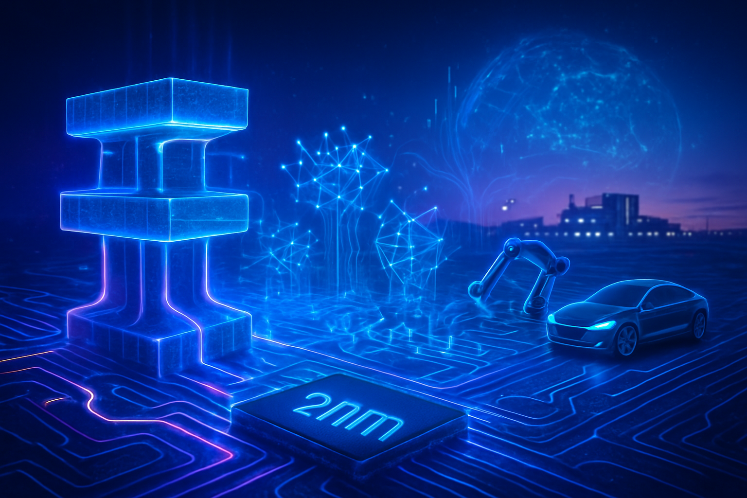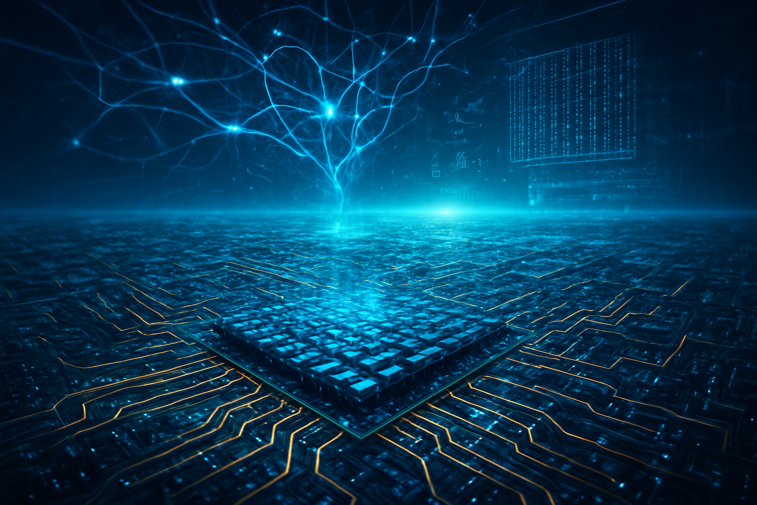
As of January 16, 2026, the global semiconductor landscape has officially entered the "2-nanometer era," marking the most significant architectural shift in silicon manufacturing in over a decade. Taiwan Semiconductor Manufacturing Company (TSMC) (NYSE: TSM) has confirmed that its N2 (2nm-class) technology node reached high-volume manufacturing (HVM) in late 2025 and is currently ramping up capacity at its state-of-the-art Fab 20 in Hsinchu and Fab 22 in Kaohsiung. This milestone represents a critical pivot point for the industry, as it marks TSMC’s transition away from the long-standing FinFET transistor structure to the revolutionary Gate-All-Around (GAA) nanosheet architecture.
The immediate significance of this development cannot be overstated. As the backbone of the AI revolution, the N2 node is expected to power the next generation of high-performance computing (HPC) and mobile processors, offering the thermal efficiency and logic density required to sustain the massive growth in generative AI. With initial 2nm capacity for 2026 already reportedly fully booked, the launch of N2 solidifies TSMC’s position as the primary gatekeeper for the world’s most advanced artificial intelligence hardware.
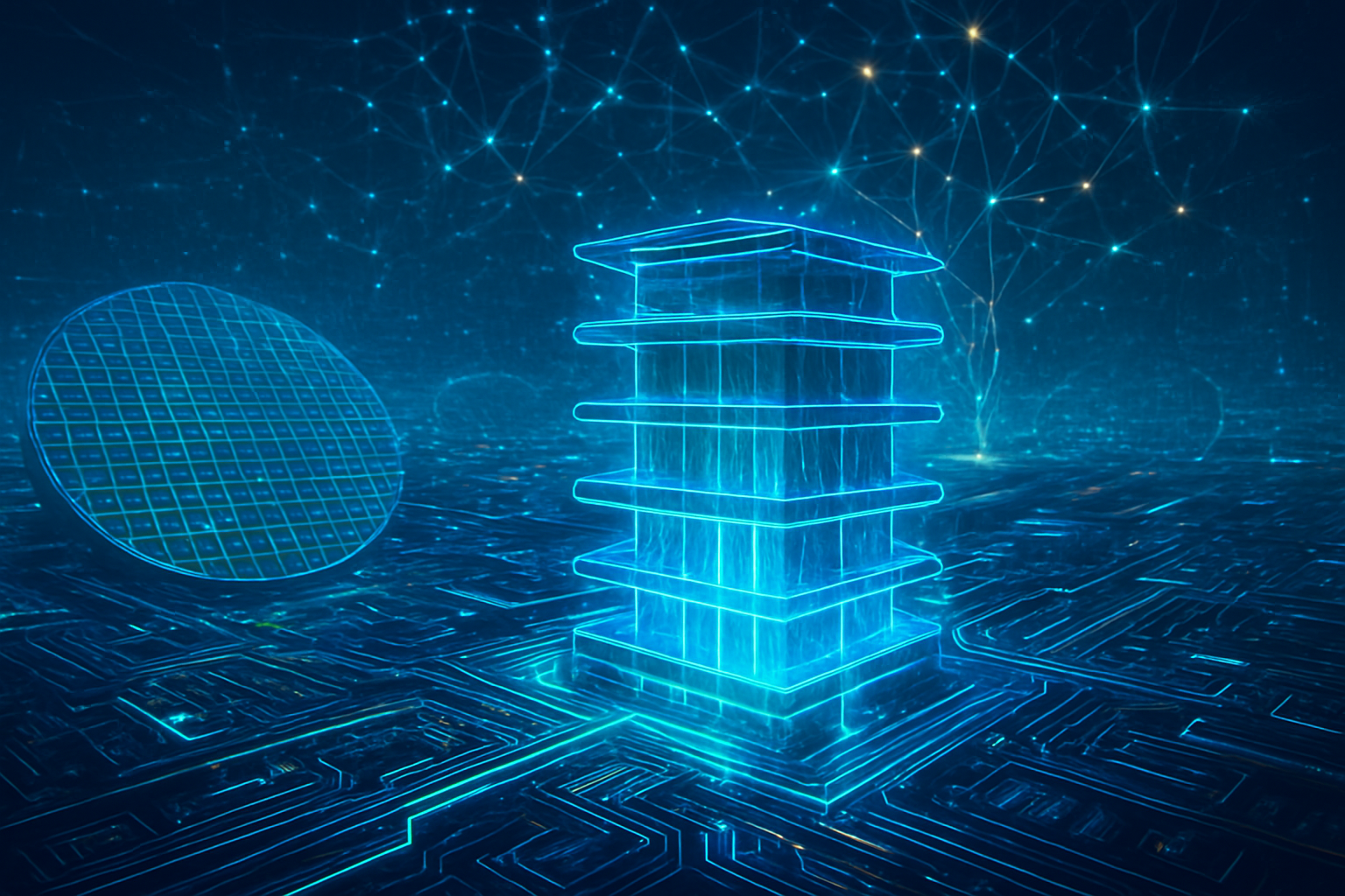
Transitioning to Nanosheets: The Technical Core of N2
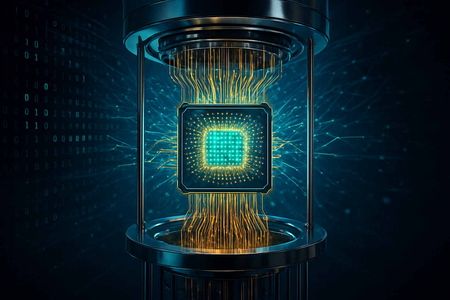
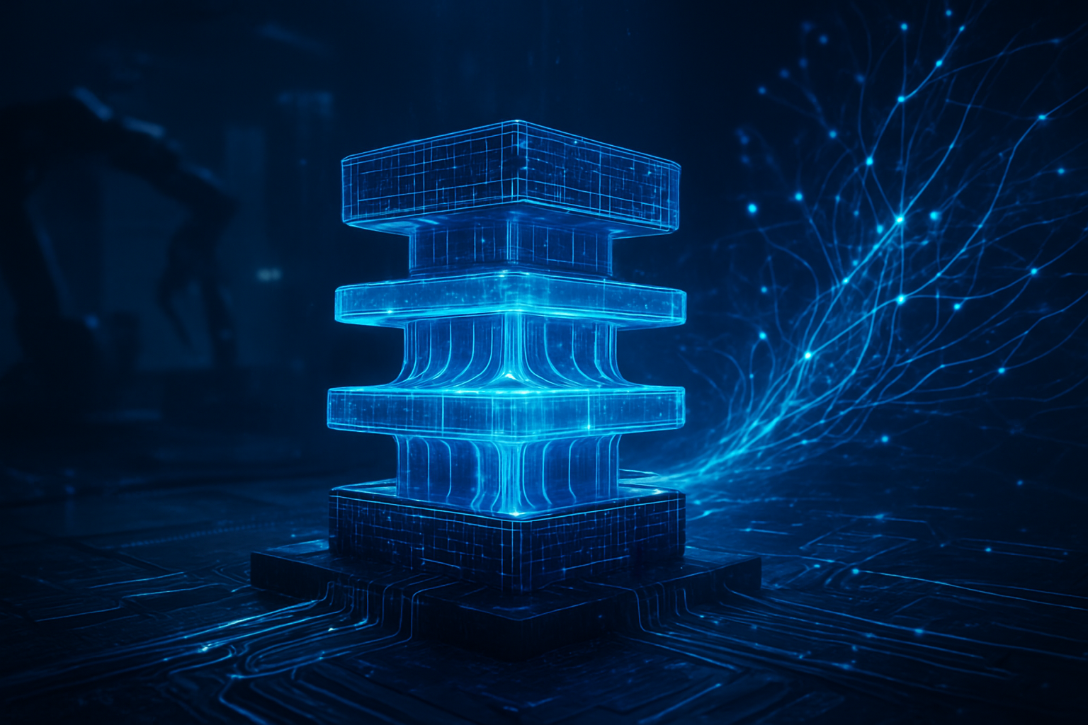
The N2 node is a technical tour de force, centered on the shift from FinFET to Gate-All-Around (GAA) nanosheet transistors. In a FinFET structure, the gate wraps around three sides of the channel; in the new N2 nanosheet architecture, the gate surrounds the channel on all four sides. This provides superior electrostatic control, which is essential for reducing "current leakage"—a major hurdle that plagued previous nodes at 3nm. By better managing the flow of electrons, TSMC has achieved a performance boost of 10–15% at the same power level, or a power reduction of 25–30% at the same speed compared to the existing N3E (3nm) node.
Beyond the transistor change, N2 introduces "Super-High-Performance Metal-Insulator-Metal" (SHPMIM) capacitors. These capacitors double the capacitance density while halving resistance, ensuring that power delivery remains stable even during the intense, high-frequency bursts of activity characteristic of AI training and inference. While TSMC has opted to delay "backside power delivery" until the N2P and A16 nodes later in 2026 and 2027, the current N2 iteration offers a 15% increase in mixed design density, making it the most compact and efficient platform for complex AI system-on-chips (SoCs).
The industry reaction has been one of cautious optimism. While TSMC's reported initial yields of 65–75% are considered high for a new architecture, the complexity of the GAA transition has led to a 3–5% price hike for 2nm wafers. Experts from the semiconductor research community note that TSMC’s "incremental" approach—stabilizing the nanosheet architecture before adding backside power—is a strategic move to ensure supply chain reliability, even as competitors like Intel (NASDAQ: INTC) push more aggressive technical roadmaps.
The 2nm Customer Race: Apple, Nvidia, and the Competitive Landscape
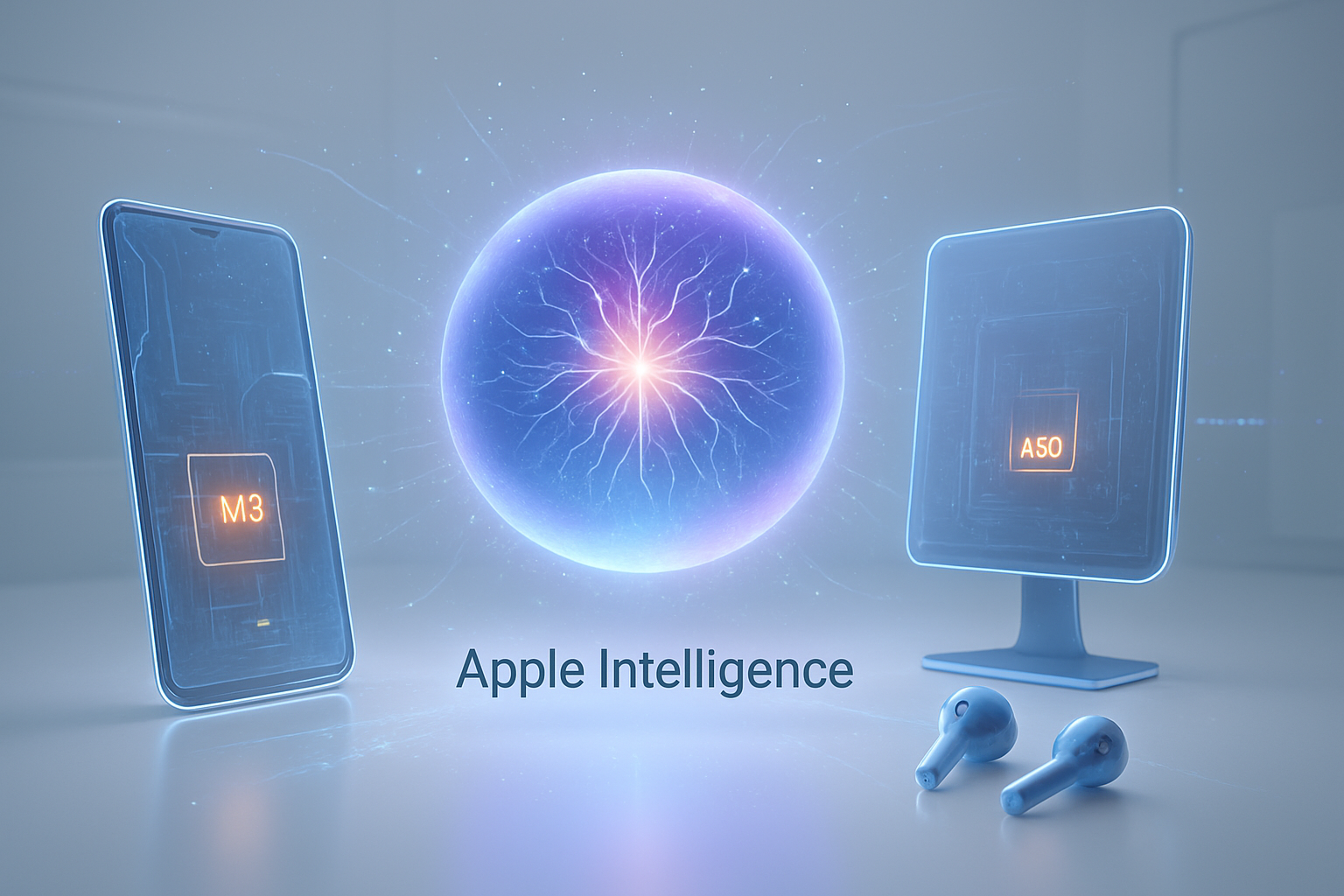
Apple (NASDAQ: AAPL) has once again secured its position as TSMC’s anchor tenant, reportedly claiming over 50% of the initial N2 capacity. This ensures that the upcoming "A20 Pro" chip, expected to debut in the iPhone 18 series in late 2026, will be the first consumer-facing 2nm processor. Beyond mobile, Apple’s M6 series for Mac and iPad is being designed on N2 to maintain a battery-life advantage in an increasingly competitive "AI PC" market. By locking in this capacity, Apple effectively prevents rivals from accessing the most efficient silicon for another year.
For Nvidia (NASDAQ: NVDA), the stakes are even higher. While the company has utilized custom 4nm and 3nm nodes for its Blackwell and Rubin architectures, the upcoming "Feynman" architecture is expected to leverage the 2nm class to drive the next leap in data center GPU performance. However, there is growing speculation that Nvidia may opt for the enhanced N2P or the 1.6nm A16 node to take advantage of backside power delivery, which is more critical for the massive power draws of AI training clusters.
The competitive landscape is more contested than in previous years. Intel (NASDAQ: INTC) recently achieved a major milestone with its 18A node, launching the "Panther Lake" processors at CES 2026. By integrating its "PowerVia" backside power technology ahead of TSMC, Intel currently claims a performance-per-watt lead in certain mobile segments. Meanwhile, Samsung Electronics (KRX: 005930) is shipping its 2nm Exynos 2600 for the Galaxy S26. Despite having more experience with GAA (which it introduced at 3nm), Samsung continues to face yield struggles, reportedly stuck at approximately 50%, making it difficult to lure "whale" customers away from the TSMC ecosystem.
Global Significance and the Energy Imperative
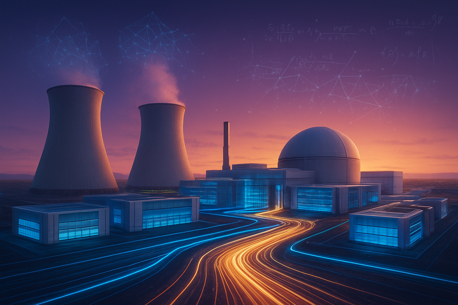
The launch of N2 fits into a broader trend where AI compute demand is outstripping energy availability. As data centers consume a growing percentage of the global power supply, the 25–30% efficiency gain offered by the 2nm node is no longer just a luxury—it is a requirement for the expansion of AI services. If the industry cannot find ways to reduce the power-per-operation, the environmental and financial costs of scaling models like GPT-5 or its successors will become prohibitive.
However, the shift to 2nm also highlights deepening geopolitical concerns. With TSMC’s primary 2nm production remaining in Taiwan, the "silicon shield" becomes even more critical to global economic stability. This has spurred a massive push for domestic manufacturing, though TSMC’s Arizona and Japan plants are currently trailing the Taiwan-based "mother fabs" by at least one full generation. The high cost of 2nm development also risks a widening "compute divide," where only the largest tech giants can afford the billions in R&D and manufacturing costs required to utilize the leading-edge nodes.
Comparatively, the transition to 2nm is as significant as the move to 3D transistors (FinFET) in 2011. It represents the end of the "classical" era of semiconductor scaling and the beginning of the "architectural" era, where performance gains are driven as much by how the transistor is built and powered as they are by how small it is.
The Road Ahead: N2P, A16, and the 1nm Horizon
Looking toward the near term, TSMC has already signaled that N2 is merely the first step in a multi-year roadmap. By late 2026, the company expects to introduce N2P, which will finally integrate "Super Power Rail" (backside power delivery). This will be followed closely by the A16 node, representing the 1.6nm class, which will introduce even more exotic materials and packaging techniques like CoWoS (Chip on Wafer on Substrate) to handle the extreme connectivity requirements of future AI clusters.
The primary challenges ahead involve the "economic limit" of Moore's Law. As wafer prices increase, software optimization and custom silicon (ASICs) will become more important than ever. Experts predict that we will see a surge in "domain-specific" architectures, where chips are designed for a single specific AI task—such as large language model inference—to maximize the efficiency of the expensive 2nm silicon.
Challenges also remain in the lithography space. As the industry moves toward "High-NA" EUV (Extreme Ultraviolet) machines, the costs of the equipment are skyrocketing. TSMC’s ability to maintain high yields while managing these astronomical costs will determine whether 2nm remains the standard for the next five years or if a new competitor can finally disrupt the status quo.
Summary of the 2nm Landscape
As we move through 2026, TSMC’s N2 node stands as the gold standard for semiconductor manufacturing. By successfully transitioning to GAA nanosheet transistors and maintaining superior yields compared to Samsung and Intel, TSMC has ensured that the next generation of AI breakthroughs will be built on its foundation. While Intel’s 18A presents a legitimate technical threat with its early adoption of backside power, TSMC’s massive ecosystem and reliability continue to make it the preferred partner for industry leaders like Apple and Nvidia.
The significance of this development in AI history is profound; the N2 node provides the physical substrate necessary for the next leap in machine intelligence. In the coming months, the industry will be watching for the first third-party benchmarks of 2nm chips and the progress of TSMC’s N2P ramp-up. The race for silicon supremacy has never been tighter, and the stakes—powering the future of human intelligence—have never been higher.
This content is intended for informational purposes only and represents analysis of current AI developments.
TokenRing AI delivers enterprise-grade solutions for multi-agent AI workflow orchestration, AI-powered development tools, and seamless remote collaboration platforms.
For more information, visit https://www.tokenring.ai/.