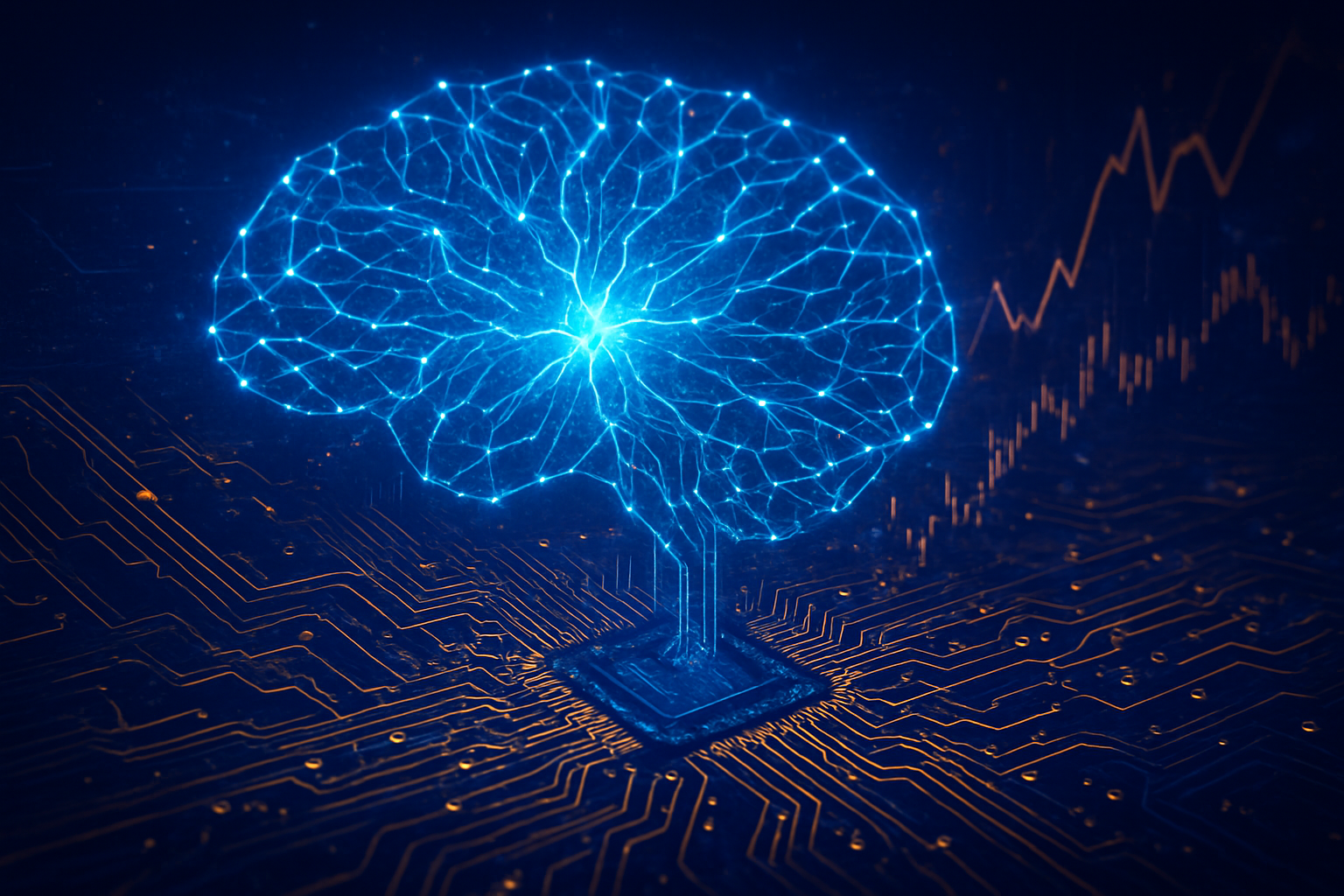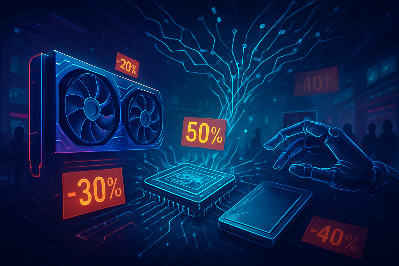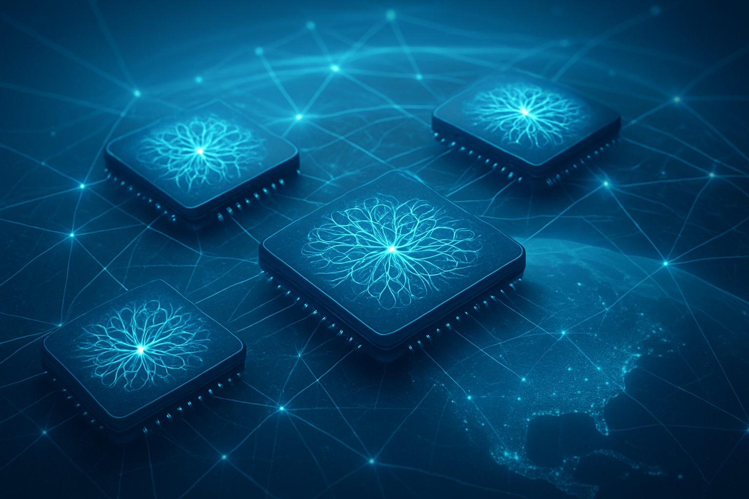
Recent advancements in chips designed for Internet of Things (IoT) devices are fundamentally transforming the landscape of connected technology. These breakthroughs, particularly in connectivity, power efficiency, and integrated edge AI, are enabling a new generation of smarter, more responsive, and sustainable devices across virtually every industry. From enhancing the capabilities of smart cities and industrial automation to revolutionizing healthcare and consumer electronics, these innovations are not merely incremental but represent a pivotal shift towards a truly intelligent and pervasive IoT ecosystem.
This wave of innovation is critical for the burgeoning IoT market, which is projected to grow substantially in the coming years. The ability to process data locally, communicate seamlessly across diverse networks, and operate for extended periods on minimal power is unlocking unprecedented potential, pushing the boundaries of what connected devices can achieve and setting the stage for a future where intelligence is embedded into the fabric of our physical world.
Technical Deep Dive: Unpacking the Engine of Tomorrow's IoT
The core of this transformation lies in specific technical advancements that redefine the capabilities of IoT chips. These innovations build upon existing technologies, offering significant improvements in performance, efficiency, and intelligence.
5G RedCap: The Smart Compromise for IoT
5G RedCap (Reduced Capability), introduced in 3GPP Release 17, is a game-changer for mid-tier IoT applications. It bridges the gap between the ultra-low-power, low-data-rate LPWAN technologies and the high-bandwidth, high-latency capabilities of full 5G enhanced Mobile Broadband (eMBB). RedCap simplifies 5G radio design by using narrower bandwidths (typically up to 20 MHz in FR1), fewer antennas (1T1R/1T2R), and lower data rates (around 250 Mbps downlink, 50 Mbps uplink) compared to advanced 5G modules. This reduction in complexity translates directly into significantly lower hardware costs, smaller chip footprints, and dramatically improved power efficiency, extending battery life for years. Unlike previous LTE Cat-1 solutions, RedCap offers better speeds and lower latency, while avoiding the power overhead of full 5G NR, making it ideal for applications like industrial sensors, video surveillance, and wearable medical devices that require more than LPWAN but less than full eMBB. 3GPP Release 18 is set to further enhance RedCap (eRedCap) for even lower-cost, ultra-low-power devices.
Wi-Fi 7: The Apex of Local Connectivity
Wi-Fi 7 (IEEE 802.11be), officially certified by the Wi-Fi Alliance in January 2024, represents a monumental leap in local wireless networking. It's designed to meet the escalating demands of dense IoT environments and data-intensive applications. Key technical differentiators include:
- Multi-Link Operation (MLO): This groundbreaking feature allows devices to simultaneously transmit and receive data across multiple frequency bands (2.4 GHz, 5 GHz, and 6 GHz). This is a stark departure from previous Wi-Fi generations that restricted devices to a single band, leading to increased overall speed, reduced latency, and enhanced connection reliability through load balancing and dynamic interference mitigation. MLO is crucial for managing the complex, concurrent connections in expanding IoT ecosystems, especially for latency-sensitive applications like AR/VR and real-time industrial automation.
- 4K QAM (4096-Quadrature Amplitude Modulation): Wi-Fi 7 introduces 4K QAM, enabling each symbol to carry 12 bits of data, a 20% increase over Wi-Fi 6's 1024-QAM. This directly translates to higher theoretical transmission rates, beneficial for bandwidth-intensive IoT applications such as 8K video streaming and high-resolution medical imaging. However, optimal performance with 4K QAM requires a very high Signal-to-Noise Ratio (SNR), meaning devices need to be in close proximity to the access point.
- 320 MHz Channel Width: Doubling Wi-Fi 6's capacity, this expanded bandwidth in the 6 GHz band allows for more data to be transmitted simultaneously, crucial for homes and enterprises with numerous smart devices.
These features collectively position Wi-Fi 7 as a cornerstone for next-generation intelligence and responsiveness in IoT.
LPWAN Evolution: The Backbone for Massive Scale
Low-Power Wide-Area Networks (LPWAN) technologies, such as Narrowband IoT (NB-IoT) and LTE-M, continue to be indispensable for connecting vast numbers of low-power devices over long distances. NB-IoT, for instance, offers extreme energy efficiency (up to 10 years on a single battery), extended coverage, and deep indoor penetration, making it ideal for applications like smart metering, environmental monitoring, and asset tracking where small, infrequent data packets are transmitted. Its evolution to Cat-NB2 (3GPP Release 14) brought improved data rates and lower latency, and it is fully forward-compatible with 5G networks, ensuring its long-term relevance for massive machine-type communications (mMTC).
Revolutionizing Power Efficiency
Power efficiency is paramount for IoT, and chip designers are employing advanced techniques:
- FinFET and GAA (Gate-All-Around) Transistors: These advanced semiconductor fabrication processes (FinFET at 22nm and below, GAA at 3nm and below) offer superior control over current flow, significantly reducing leakage current and improving switching speed compared to older planar transistors. This directly translates to lower power consumption and higher performance.
- FD-SOI (Fully Depleted Silicon-On-Insulator): This technology eliminates doping, reducing leakage currents and allowing transistors to operate at very low voltages, enhancing power efficiency and enabling faster switching. It's particularly beneficial for integrating analog and digital circuits on a single chip, crucial for compact IoT solutions.
- DVFS (Dynamic Voltage and Frequency Scaling): This power management technique dynamically adjusts a processor's voltage and frequency based on workload, significantly reducing dynamic power consumption during idle or low-activity periods. AI and machine learning are increasingly integrated into DVFS for anticipatory power management, further optimizing energy savings.
- Specialized Architectures: Application-Specific Integrated Circuits (ASICs) and dedicated AI accelerators (like Neural Processing Units – NPUs) are custom-designed for AI computations. They prioritize parallel processing and efficient data flow, offering superior power-to-performance ratios for AI workloads at the edge compared to general-purpose CPUs.
Initial reactions from the AI research community and industry experts are overwhelmingly positive. 5G RedCap is seen as a "sweet spot" for everyday IoT, enabling billions of devices to benefit from 5G's reliability and scalability with lower complexity and cost. Wi-Fi 7 is hailed as a "game-changer" for its promise of faster, more reliable, and lower-latency connectivity for advanced IoT applications. FD-SOI is gaining recognition as a key enabler for AI-driven IoT due to its unique power efficiency benefits, and specialized AI chips are considered critical for the next phase of AI breakthroughs, especially in enabling AI at the "edge."
Corporate Chessboard: Shifting Fortunes for Tech Giants and Startups
The rapid evolution of IoT chip technology is creating a dynamic competitive landscape, offering immense opportunities for some and posing significant challenges for others. Tech giants, AI companies, and nimble startups are all vying for position in this burgeoning market.
Tech Giants Lead the Charge:
Major tech players with deep pockets and established ecosystems are strategically positioned to capitalize on these advancements.
- Qualcomm (NASDAQ: QCOM) is a dominant force, leveraging its expertise in 5G and Wi-Fi to deliver comprehensive IoT solutions. Their QCC730 Wi-Fi SoC, launched in April 2024, boasts up to 88% lower power usage, while their QCS8550/QCM8550 processors integrate extreme edge AI processing and Wi-Fi 7 for demanding applications like autonomous mobile robots. Qualcomm's strategy is to be a key enabler of the AI-driven connected future, expanding beyond smartphones into automotive and industrial IoT.
- Intel (NASDAQ: INTC) is actively pushing into the IoT space with new Core, Celeron, Pentium, and Atom processors designed for the edge, incorporating AI, security, and real-time capabilities. Their "Intel NB-IoT Modules," announced in January 2024, promise up to 90% power reduction for long-range, low-power applications. Intel's focus is on simplifying connectivity and enhancing data security for IoT deployments.
- NVIDIA (NASDAQ: NVDA) is a powerhouse in edge AI, offering a full stack from high-performance GPUs and embedded modules (like Jetson) to networking and software platforms. NVIDIA's strategy is to be the foundational AI platform for the AI-IoT ecosystem, enabling smart vehicles, intelligent factories, and AI-assisted healthcare.
- Arm Holdings (NASDAQ: ARM) remains foundational, with its power-efficient RISC architecture underpinning countless IoT devices. Arm's designs, known for high performance on minimal power, are crucial for the growing AI and IoT sectors, with major clients like Apple (NASDAQ: AAPL) and Samsung (KRX: 005930) leveraging Arm designs for their AI and IoT strategies.
- Google (NASDAQ: GOOGL) offers its Edge TPU, a custom ASIC for efficient TensorFlow Lite ML model execution at the edge, and Google Cloud IoT Edge software to extend cloud ML capabilities to devices.
- Microsoft (NASDAQ: MSFT) provides the Azure IoT suite, including IoT Hub for secure connectivity and Azure IoT Edge for extending cloud intelligence to edge devices, enabling local data processing and AI features.
These tech giants will intensify competition, leveraging their full-stack offerings, from hardware to cloud platforms and AI services. Their established ecosystems, financial power, and influence on standards provide significant advantages in scaling IoT solutions globally.
AI Companies and Startups: Niche Innovation and Disruption:
AI companies, particularly those specializing in model optimization for constrained hardware, stand to benefit significantly. The ability to deploy AI models directly on devices leads to faster inference, autonomous operation, and real-time decision-making, opening new markets in industrial automation, healthcare, and smart cities. Companies that can offer "AI-as-a-chip" or highly optimized software-hardware bundles will gain a competitive edge.
Startups, while facing stiff competition, have immense opportunities. Advancements like 5G RedCap and LPWAN lower the cost and power requirements for connectivity, making it feasible for startups to develop solutions for previously cost-prohibitive use cases. They can focus on highly specialized edge AI algorithms and applications for specific industry pain points, leveraging open-source ecosystems and development kits. Innovative startups could disrupt established markets by introducing novel IoT devices or services that leverage these chip advancements in unexpected ways, especially in niche sectors where large players move slowly. Strategic partnerships with larger companies for distribution or platform services will be crucial for scaling.
The shift towards edge AI could disrupt traditional cloud-centric AI deployment models, requiring AI companies to adapt to distributed intelligence. While tech giants lead with comprehensive solutions, their complexity might leave niches open for agile, specialized players offering customized or ultra-low-cost solutions.
A New Era of Pervasive Intelligence: Broader Significance and Societal Impact
The advancements in IoT chips are more than just technical upgrades; they signify a profound shift in the broader AI landscape, ushering in an era of pervasive, distributed intelligence with far-reaching societal impacts and critical considerations.
Fitting into the Broader AI Landscape:
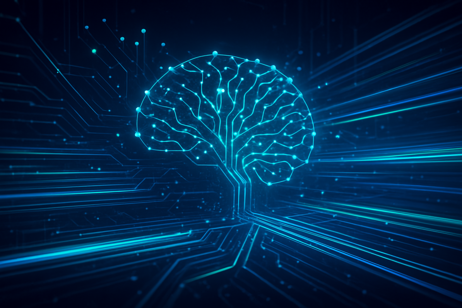
This wave of innovation is fundamentally driving the decentralization of AI. Historically, AI has largely been cloud-centric, relying on powerful data centers for computation. The advent of efficient edge AI chips, combined with advanced connectivity, enables complex AI computations to occur directly on devices. This is a "fundamental re-architecture" of how AI operates, mirroring the historical shift from mainframe computing to personal computing. It allows for real-time decision-making, crucial for applications where immediate responses are vital (e.g., autonomous systems, industrial automation), and significantly reduces reliance on continuous cloud connectivity, fostering new paradigms for AI applications that are more resilient, responsive, and data-private. The ability of these chips to handle high volumes of data locally and efficiently allows for the deployment of billions of intelligent IoT devices, vastly expanding the reach and impact of AI, making it truly ubiquitous.
Societal Impacts:
The convergence of AI and IoT (AIoT), propelled by these chip advancements, promises transformative societal impacts:
- Economic Growth and Efficiency: AIoT will drive unprecedented efficiency in sectors like healthcare, transportation, energy management, smart cities, and agriculture. Smart factories will leverage AIoT for faster, more accurate production, predictive maintenance, and real-time monitoring, boosting productivity and reducing costs.
- Improved Quality of Life: Smart cities will utilize AIoT for intelligent traffic management, waste optimization, environmental monitoring, and public safety. In healthcare, wearables and medical devices enabled by 5G RedCap and edge AI will provide real-time patient monitoring and support personalized treatment plans, potentially creating "virtual hospital wards."
- Workforce Transformation: While AIoT automates routine tasks, potentially leading to job displacement in some areas, it also creates new jobs in technology fields and frees up the human workforce for tasks requiring creativity and empathy.
- Sustainability: Energy-efficient chips and smart IoT solutions will contribute significantly to reducing global energy consumption and carbon emissions, supporting Net Zero operational goals across industries.
Potential Concerns:
Despite the positive outlook, significant concerns must be proactively addressed:
- Security: The massive increase in connected IoT devices vastly expands the attack surface for cyber threats. Many IoT devices have minimal security due to cost and speed pressures, making them vulnerable to hacking, data breaches, and disruption of critical infrastructure. The evolution of 5G and AI also introduces new, unknown attack vectors, including AI-driven attacks. Hardware-based security, secure boot, and cryptographic accelerators are becoming essential.
- Privacy: The proliferation of IoT devices and edge AI leads to the collection and processing of vast amounts of personal and sensitive data. Concerns regarding data ownership, usage, and transparent consent mechanisms are paramount. While local processing via edge AI can mitigate some risks, robust security is still needed to prevent unauthorized access. The widespread deployment of smart cameras and sensors also raises concerns about surveillance.
- Ethical AI: The integration of AI into IoT devices brings complex ethical considerations. AI systems can inherit and amplify biases, potentially leading to discriminatory outcomes. Determining accountability when AI-driven IoT devices make errors or cause harm is a significant legal and ethical challenge, compounded by the "black box" problem of opaque AI algorithms. Questions about human control over increasingly autonomous AIoT systems also arise.
Comparisons to Previous AI Milestones:
This era of intelligent IoT chips can be compared to several transformative milestones:
- Shift to Distributed Intelligence: Similar to the shift from centralized mainframes to personal computing, or from centralized internet servers to the mobile internet, edge AI decentralizes intelligence, embedding it into billions of everyday objects.
- Pervasive Computing, Now Intelligent: It realizes the early visions of pervasive computing but with a crucial difference: the devices are not just connected; they are intelligent, making AI truly ubiquitous in the physical world.
- Beyond Moore's Law: While Moore's Law has driven computing for decades, the specialization of AI chips (e.g., NPUs, ASICs) allows for performance gains through architectural innovations rather than solely relying on transistor scaling, akin to the development of GPUs for parallel processing.
- Real-time Interaction with the Physical World: Unlike previous AI breakthroughs that often operated in abstract domains, current advancements enable AI to interact directly, autonomously, and in real-time with the physical environment at an unprecedented scale.
The Horizon: Future Developments and Expert Predictions
The trajectory of IoT chip development points towards an increasingly intelligent, autonomous, and integrated future. Both near-term and long-term developments promise to push the boundaries of what connected devices can achieve.
Near-term Developments (next 1-5 years):
By 2026, several key trends are expected to solidify:
- Accelerated Edge AI Integration: Edge AI will become a standard feature in many IoT sensors, modules, and gateways. Neural Processing Units (NPUs) and AI-capable cores will be integrated into mainstream IoT designs, enabling local data processing for anomaly detection, small-model vision, and local audio intelligence, reducing reliance on cloud inference.
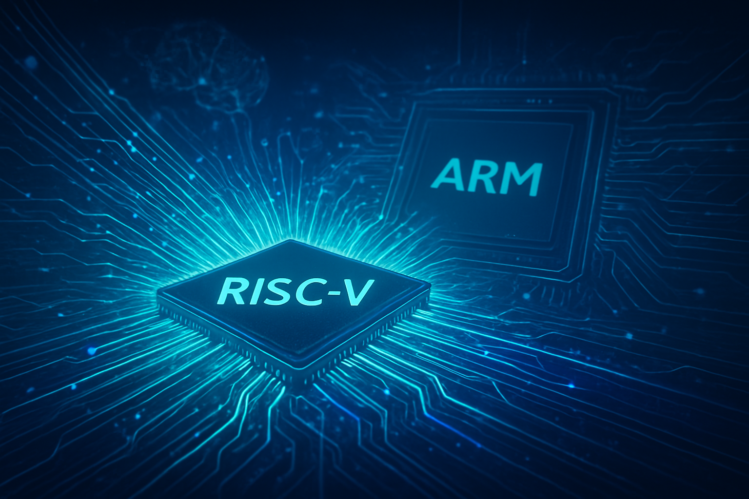
- Chiplet-based and RISC-V Architectures: The adoption of modular chiplet designs and open-standard RISC-V-based IoT chips is predicted to increase significantly. Chiplets allow for reduced engineering effort and faster development cycles, while RISC-V offers flexibility and customization, fostering innovation and reducing vendor lock-in.
- Carbon-Aware Design: More IoT chips will be designed with sustainability in mind, focusing on energy-efficient designs to support global carbon reduction goals.
- Early Post-Quantum Cryptography (PQC): Early pilots of PQC-ready security blocks are expected in higher-value IoT chips, addressing emerging threats from quantum computing, particularly for long-lifecycle devices in critical infrastructure.
- Specialized Chips: Expect a proliferation of highly specialized chips tailored for specific IoT systems and use cases, leveraging the advantages of edge computing and AI.
Long-term Developments:
Looking further ahead, revolutionary paradigms are on the horizon:
- Ubiquitous and Pervasive AI: The long-term impact will be transformative, leading to AI embedded into nearly every device and system, from tiny IoT sensors to advanced robotics, creating a truly intelligent environment.
- 6G Connectivity: Research into 6G technology is already underway, promising even higher speeds, lower latency, and more reliable connections, which will further enhance IoT system capabilities and enable entirely new applications.
- Quantum Computing Integration: While still in early stages, quantum computing has the potential to revolutionize how data is processed and analyzed in IoT, offering unprecedented optimization capabilities for complex problems like supply chain management and enhancing cryptographic security.
- New Materials and Architectures: Continued research into emerging semiconductor materials like Gallium Nitride (GaN) and Silicon Carbide (SiC) will enable more compact and efficient power electronics and high-frequency AI processing at the edge. Innovations in 2D materials and advanced System-on-Chip (SoC) integration will further enhance energy efficiency and scalability.
Challenges on the Horizon:
Despite the promising outlook, several challenges must be addressed:
- Security and Privacy: These remain paramount concerns, requiring robust hardware-enforced security, secure boot processes, and tamper-resistant identities at the silicon level.
- Interoperability and Standardization: The fragmented nature of the IoT market, with diverse devices and protocols, continues to hinder seamless integration. Unified standards are crucial for widespread adoption.
- Cost and Complexity: Reducing manufacturing costs while integrating advanced features like AI and robust security remains a balancing act. Managing the complexity of interconnected components and integrating with existing IT infrastructure is also a significant hurdle.
- Talent Gap: A shortage of skilled resources for IoT application development could hinder progress.
Expert Predictions:
Experts anticipate robust growth for the global IoT chip market, driven by the proliferation of smart devices and increasing adoption across industries. Edge AI is expected to accelerate significantly, becoming a default feature in many devices. Architectural shifts towards chiplet-based and RISC-V designs will offer OEMs greater flexibility. Furthermore, AI is predicted to play a crucial role in the design of IoT chips themselves, acting as "copilots" for tasks like verification and physical design exploration, reducing complexity and lowering barriers to entry for AI in mass-market IoT devices. Hardware security evolution, including PQC-ready blocks, will become standard in critical IoT applications, and sustainability will increasingly influence design choices.
The Intelligent Future: A Comprehensive Wrap-Up
The ongoing advancements in IoT chip technology—a powerful confluence of enhanced connectivity, unparalleled power efficiency, and integrated edge AI—are not merely incremental improvements but represent a defining moment in the history of artificial intelligence and connected computing. As of December 15, 2025, these developments are rapidly moving from research labs into commercial deployment, setting the stage for a truly intelligent and autonomous future.
Key Takeaways:
The core message is clear: IoT devices are evolving from simple data collectors to intelligent, autonomous decision-makers.
- Connectivity Redefined: 5G RedCap is filling a critical gap for mid-tier IoT, offering 5G benefits with reduced cost and power. Wi-Fi 7, with its Multi-Link Operation (MLO) and 4K QAM, is delivering unprecedented speed and reliability for high-density, data-intensive local IoT. LPWAN technologies continue to provide the low-power, long-range backbone for massive deployments.
- Power Efficiency as a Foundation: Innovations in chip architectures (like FeFET cells, FinFET, GAA, FD-SOI) and design techniques (DVFS) are dramatically extending battery life and reducing the energy footprint of billions of devices, making widespread, sustainable IoT feasible.
- Edge AI as the Brain: Integrating AI directly into chips allows for real-time processing, reduced latency, enhanced privacy, and autonomous operation, transforming devices into smart agents that can act independently of the cloud. This is driving a "fundamental re-architecture" of how AI operates, decentralizing intelligence.
Significance in AI History:
These advancements signify a pivotal shift towards ubiquitous AI. No longer confined to data centers or high-power devices, AI is becoming embedded into the fabric of everyday objects. This decentralization of intelligence enables real-time interaction with the physical world at an unprecedented scale, moving beyond abstract analytical domains to directly impact physical processes and decisions. It's a journey akin to the shift from mainframe computing to personal computing, bringing powerful AI capabilities to the "edge" and democratizing access to sophisticated intelligence.
Long-Term Impact:
The long-term impact will be transformative, ushering in an era of hyper-connected, intelligent environments. Industries from healthcare and manufacturing to smart cities and agriculture will be revolutionized, leading to increased efficiency, new business models, and significant strides in sustainability. Enhanced security and privacy, through local data processing and hardware-enforced measures, will also become more inherent in IoT systems. This era promises a future where our environments are not just connected, but truly intelligent and responsive.
What to Watch For:
In the coming weeks and months, several key indicators will signal the pace and direction of this evolution:
- Widespread Wi-Fi 7 Adoption: Observe the increasing availability and performance of Wi-Fi 7 devices and infrastructure, particularly in high-density IoT environments.
- 5G RedCap Commercialization: Track the rollout of 5G RedCap networks and the proliferation of devices leveraging this technology in industrial, smart city, and wearable applications.
- Specialized AI Chip Innovation: Look for announcements of new specialized chips designed for low-power edge AI workloads, especially those leveraging chiplets and RISC-V architectures, which are predicted to see significant growth.
- Hardware Security Enhancements: Monitor the broader adoption of robust hardware-enforced security features and early pilots of Post-Quantum Cryptography (PQC)-ready security blocks in critical IoT devices.
- Hybrid Connectivity Solutions: Keep an eye on the integration of hybrid connectivity models, combining cellular, LPWAN, and satellite networks, especially with standards like GSMA SGP.32 eSIM launching in 2025.
- Growth of AIoT Markets: Track the continued substantial growth of the Edge AI market and the emerging generative AI in IoT market, and the innovative applications they enable.
This content is intended for informational purposes only and represents analysis of current AI developments.
TokenRing AI delivers enterprise-grade solutions for multi-agent AI workflow orchestration, AI-powered development tools, and seamless remote collaboration platforms.
For more information, visit https://www.tokenring.ai/.