Tag: Technology News

  • The Dawn of the Android Age: Figure AI Ignites the Humanoid Robotics Revolution

    The Dawn of the Android Age: Figure AI Ignites the Humanoid Robotics Revolution

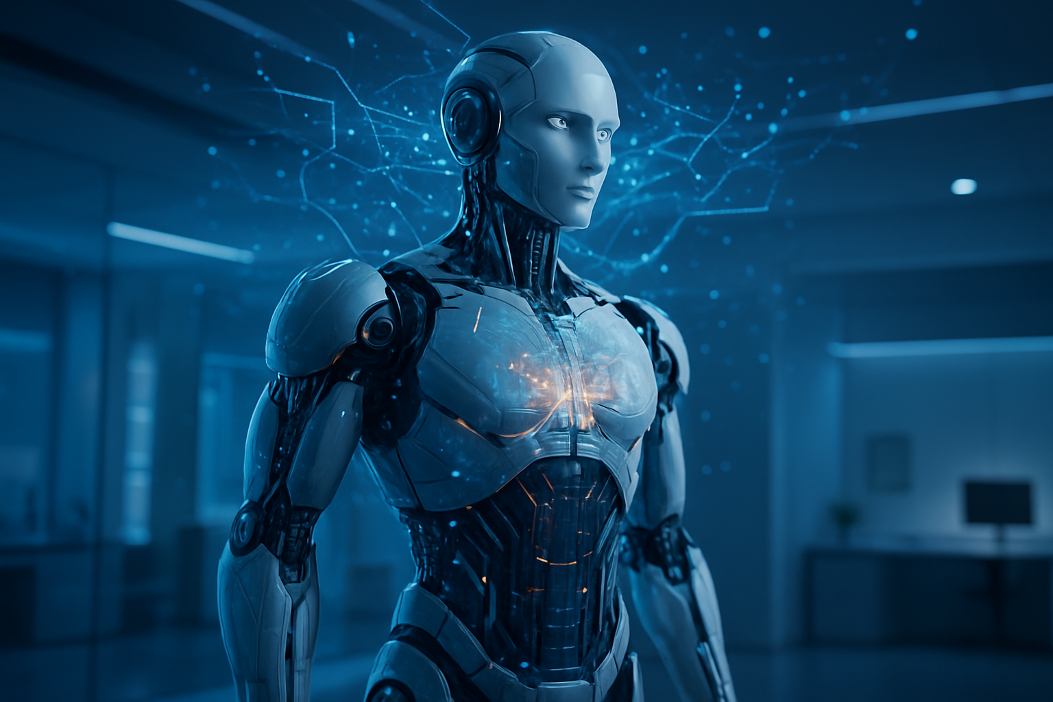
    Brett Adcock, the visionary CEO of Figure AI (NASDAQ: FGR), is not one to mince words when describing the future of technology. He emphatically declares humanoid robotics as "the next major technological revolution," a paradigm shift he believes will be as profound as the advent of the internet itself. This bold assertion, coupled with Figure AI's rapid advancements and staggering valuations, is sending ripples across the tech industry, signaling an impending era where autonomous, human-like machines could fundamentally transform global economies and daily life. Adcock envisions an "age of abundance" driven by these versatile robots, making physical labor optional and reshaping the very fabric of society.

    Figure AI's aggressive pursuit of general-purpose humanoid robots is not merely theoretical; it is backed by significant technological breakthroughs and substantial investment. The company's mission to "expand human capabilities through advanced AI" by deploying autonomous humanoids globally aims to tackle critical labor shortages, eliminate hazardous jobs, and ultimately enhance the quality of life for future generations. This ambition places Figure AI at the forefront of a burgeoning industry poised to redefine the human-machine interface in the physical world.

    Unpacking Figure AI's Autonomous Marvels: A Technical Deep Dive

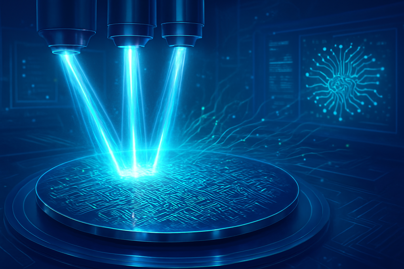
    Figure AI's journey from concept to cutting-edge reality has been remarkably swift, marked by the rapid iteration of its humanoid prototypes. The company unveiled its first prototype, Figure 01, in 2022, quickly followed by Figure 02 in 2024, which showcased enhanced mobility and dexterity. The latest iteration, Figure 03, launched in October 2025, represents a significant leap forward, specifically designed for home environments with advanced vision-language-action (VLA) AI. This model incorporates features like soft goods for safer interaction, wireless charging, and improved audio systems for sophisticated voice reasoning, pushing the boundaries of what a domestic robot can achieve.

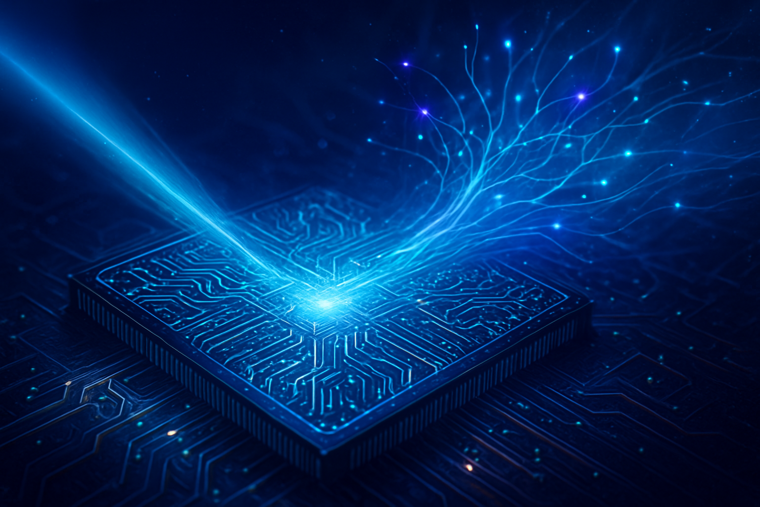
    At the heart of Figure's robotic capabilities lies its proprietary "Helix" neural network. This advanced VLA model is central to enabling the robots to perform complex, autonomous tasks, even those involving deformable objects like laundry. Demonstrations have shown Figure's robots adeptly folding clothes, loading dishwashers, and executing uninterrupted logistics work for extended periods. Unlike many existing robotic solutions that rely on teleoperation or pre-programmed, narrow tasks, Figure AI's unwavering commitment is to full autonomy. Brett Adcock has explicitly stated that the company "will not teleoperate" its robots in the market, insisting that products will only launch at scale when they are fully autonomous, a stance that sets a high bar for the industry and underscores their focus on true general-purpose intelligence.

    This approach significantly differentiates Figure AI from previous robotic endeavors. While industrial robots have long excelled at repetitive tasks in controlled environments, and earlier humanoid projects often struggled with real-world adaptability and general intelligence, Figure AI aims to create machines that can learn, adapt, and interact seamlessly within unstructured human environments. Initial reactions from the AI research community and industry experts have been a mix of excitement and cautious optimism. The substantial funding from tech giants like Microsoft (NASDAQ: MSFT), OpenAI, Nvidia (NASDAQ: NVDA), and Jeff Bezos underscores the belief in Figure AI's potential, even as experts acknowledge the immense challenges in scaling truly autonomous, general-purpose humanoids. The ability of Figure 03 to perform household chores autonomously is seen as a crucial step towards validating Adcock's vision of robots in every home within "single-digit years."

    Reshaping the AI Landscape: Competitive Dynamics and Market Disruption

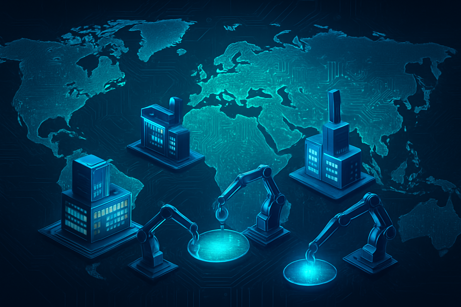
    Figure AI's aggressive push into humanoid robotics is poised to profoundly impact the competitive landscape for AI companies, tech giants, and startups alike. Companies that stand to benefit most directly are those capable of integrating advanced AI with sophisticated hardware, a niche Figure AI has carved out for itself. Beyond Figure AI, established players like Boston Dynamics (a subsidiary of Hyundai Motor Group), Tesla (NASDAQ: TSLA) with its Optimus project, and emerging startups in the robotics space are all vying for leadership in what Adcock terms a "humanoid arms race." The sheer scale of investment in Figure AI, surpassing $1 billion and valuing the company at $39 billion, highlights the intense competition and the perceived market opportunity.

    The competitive implications for major AI labs and tech companies are immense. Companies like Google (NASDAQ: GOOGL), Amazon (NASDAQ: AMZN), and Microsoft, already heavily invested in AI research, are now facing a new frontier where their software prowess must converge with physical embodiment. Those with strong AI development capabilities but lacking robust hardware expertise may seek partnerships or acquisitions to stay competitive. Conversely, hardware-focused companies without leading AI could find themselves at a disadvantage. Figure AI's strategic partnerships, such as the commercial deployment of Figure 02 robots at BMW's (FWB: BMW) South Carolina facility in 2024, demonstrate the immediate commercial viability and potential for disruption in manufacturing and logistics.

    This development poses a significant disruption to existing products and services. Industries reliant on manual labor, from logistics and manufacturing to elder care and domestic services, could see radical transformations. The promise of humanoids making physical labor optional could lead to a dramatic reduction in the cost of goods and services, forcing companies across various sectors to re-evaluate their operational models. For startups, the challenge lies in finding defensible niches or developing unique AI models or hardware components that can integrate with or compete against the likes of Figure AI. Market positioning will hinge on the ability to demonstrate practical, safe, and scalable autonomous capabilities, with Figure AI's focus on fully autonomous, general-purpose robots setting a high bar.

    The Wider Significance: Abundance, Ethics, and the Humanoid Era

    The emergence of capable humanoid robots like those from Figure AI fits squarely into the broader AI landscape as a critical next step in the evolution of artificial intelligence from digital to embodied intelligence. While large language models (LLMs) and generative AI have dominated recent headlines, humanoid robotics represents the physical manifestation of AI's capabilities, bridging the gap between virtual intelligence and real-world interaction. This development is seen by many, including Adcock, as a direct path to an "age of abundance," where repetitive, dangerous, or undesirable jobs are handled by machines, freeing humans for more creative and fulfilling pursuits.

    The potential impacts are vast and multifaceted. Economically, humanoids could drive unprecedented productivity gains, alleviate labor shortages in aging populations, and significantly lower production costs. Socially, they could redefine work, leisure, and even the structure of households. However, these profound changes also bring potential concerns. The most prominent is job displacement, a challenge that Adcock suggests could be mitigated by discussions around universal basic income. Ethical considerations surrounding the safety of human-robot interaction, data privacy, and the societal integration of intelligent machines become increasingly urgent as these robots move from factories to homes. The notion of "10 billion humanoids on Earth" within decades, as Adcock predicts, necessitates robust regulatory frameworks and societal dialogues.

    Comparing this to previous AI milestones, the current trajectory of humanoid robotics feels akin to the early days of digital AI or the internet's nascent stages. Just as the internet fundamentally changed information access and communication, humanoid robots have the potential to fundamentally alter physical labor and interaction with the material world. The ability of Figure 03 to perform complex domestic tasks autonomously is a tangible step, reminiscent of early internet applications that hinted at the massive future potential. This is not just an incremental improvement; it's a foundational shift towards truly general-purpose physical AI.

    The Horizon of Embodied Intelligence: Future Developments and Challenges

    Looking ahead, the near-term and long-term developments in humanoid robotics are poised for rapid acceleration. In the near term, experts predict a continued focus on refining dexterity, improving navigation in unstructured environments, and enhancing human-robot collaboration. Figure AI's plan to ship 100,000 units within the next four years, alongside establishing a high-volume manufacturing facility, BotQ, with an initial capacity of 12,000 robots annually, indicates an imminent scale-up. The strategic collection of massive amounts of real-world data, including partnering with Brookfield to gather human movement footage from 100,000 homes, is critical for training more robust and adaptable AI models. Adcock expects robots to enter the commercial workforce "now and in the next like year or two," with the home market "definitely solvable" within this decade, aiming for Figure 03 in select homes by 2026.

    Potential applications and use cases on the horizon are boundless. Beyond logistics and manufacturing, humanoids could serve as assistants in healthcare, companions for the elderly, educators, and even disaster relief responders. The vision of a "universal interface in the physical world" suggests a future where these robots can adapt to virtually any task currently performed by humans. However, significant challenges remain. Foremost among these is achieving true, robust general intelligence that can handle the unpredictability and nuances of the real world without constant human supervision. The "sim-to-real" gap, where AI trained in simulations struggles in physical environments, is a persistent hurdle. Safety, ethical integration, and public acceptance are also crucial challenges that need to be addressed through rigorous testing, transparent development, and public education.

    Experts predict that the next major breakthroughs will come from advancements in AI's ability to reason, plan, and learn from limited data, coupled with more agile and durable hardware. The convergence of advanced sensors, powerful onboard computing, and sophisticated motor control will continue to drive progress. What to watch for next includes more sophisticated demonstrations of complex, multi-step tasks in varied environments, deeper integration of multimodal AI (vision, language, touch), and the deployment of humanoids in increasingly public and domestic settings.

    A New Era Unveiled: The Humanoid Robotics Revolution Takes Hold

    In summary, Brett Adcock's declaration of humanoid robotics as the "next major technological revolution" is more than just hyperbole; it is a vision rapidly being materialized by companies like Figure AI. Key takeaways include Figure AI's swift development of autonomous humanoids like Figure 03, powered by advanced VLA models like Helix, and its unwavering commitment to full autonomy over teleoperation. This development is poised to disrupt industries, create new economic opportunities, and profoundly reshape the relationship between humans and technology.

    The significance of this development in AI history cannot be overstated. It represents a pivotal moment where AI transitions from primarily digital applications to widespread physical embodiment, promising an "age of abundance" by making physical labor optional. While challenges related to job displacement, ethical integration, and achieving robust general intelligence persist, the momentum behind humanoid robotics is undeniable. This is not merely an incremental step but a foundational shift towards a future where intelligent, human-like machines are integral to our daily lives.

    In the coming weeks and months, observers should watch for further demonstrations of Figure AI's robots in increasingly complex and unstructured environments, announcements of new commercial partnerships, and the initial deployment of Figure 03 in select home environments. The competitive landscape will intensify, with other tech giants and startups accelerating their own humanoid initiatives. The dialogue around the societal implications of widespread humanoid adoption will also grow, making this a critical area of innovation and public discourse. The age of the android is not just coming; it is already here, and its implications are just beginning to unfold.


    This content is intended for informational purposes only and represents analysis of current AI developments.

    TokenRing AI delivers enterprise-grade solutions for multi-agent AI workflow orchestration, AI-powered development tools, and seamless remote collaboration platforms.
    For more information, visit https://www.tokenring.ai/.

  • Arm’s Architecture Ascends: Powering the Next Wave of AI from Edge to Cloud

    Arm’s Architecture Ascends: Powering the Next Wave of AI from Edge to Cloud

    Arm Holdings plc (NASDAQ: ARM) is rapidly cementing its position as the foundational intellectual property (IP) provider for the design and architecture of next-generation artificial intelligence (AI) chips. As the AI landscape explodes with innovation, from sophisticated large language models (LLMs) in data centers to real-time inference on myriad edge devices, Arm's energy-efficient and highly scalable architectures are proving indispensable, driving a profound shift in how AI hardware is conceived and deployed. This strategic expansion underscores Arm's critical role in shaping the future of AI computing, offering solutions that balance performance with unprecedented power efficiency across the entire spectrum of AI applications.

    The company's widespread influence is not merely a projection but a tangible reality, evidenced by its deepening integration into the product roadmaps of tech giants and innovative startups alike. Arm's IP, encompassing its renowned CPU architectures like Cortex-M, Cortex-A, and Neoverse, alongside its specialized Ethos Neural Processing Units (NPUs), is becoming the bedrock for a diverse array of AI hardware. This pervasive adoption signals a significant inflection point, as the demand for sustainable and high-performing AI solutions increasingly prioritizes Arm's architectural advantages.

    Technical Foundations: Arm's Blueprint for AI Innovation

    Arm's strategic brilliance lies in its ability to offer a tailored yet cohesive set of IP solutions that cater to the vastly different computational demands of AI. For the burgeoning field of edge AI, where power consumption and latency are paramount, Arm provides solutions like its Cortex-M and Cortex-A CPUs, tightly integrated with Ethos-U NPUs. The Ethos-U series, including the advanced Ethos-U85, is specifically engineered to accelerate machine learning inference, drastically reducing processing time and memory footprints on microcontrollers and Systems-on-Chip (SoCs). For instance, the Arm Cortex-M52 processor, featuring Arm Helium technology, significantly boosts digital signal processing (DSP) and ML performance for battery-powered IoT devices without the prohibitive cost of dedicated accelerators. The recently unveiled Armv9 edge AI platform, incorporating the new Cortex-A320 and Ethos-U85, promises up to 10 times the machine learning performance of its predecessors, enabling on-device AI models with over a billion parameters and fostering real-time intelligence in smart homes, healthcare, and industrial automation.

    In stark contrast, for the demanding environments of data centers, Arm's Neoverse family delivers scalable, power-efficient computing platforms crucial for generative AI and LLM inference and training. Neoverse CPUs are designed for optimal pairing with accelerators such as GPUs and NPUs, providing high throughput and a lower total cost of ownership (TCO). The Neoverse V3 CPU, for example, offers double-digit performance improvements over its predecessors, targeting maximum performance in cloud, high-performance computing (HPC), and machine learning workloads. This modular approach, further enhanced by Arm's Compute Subsystems (CSS) for Neoverse, accelerates the development of workload-optimized, customized silicon, streamlining the creation of efficient data center infrastructure. This strategic divergence from traditional monolithic architectures, coupled with a relentless focus on energy efficiency, positions Arm as a key enabler for the sustainable scaling of AI compute. Initial reactions from the AI research community and industry experts have been overwhelmingly positive, citing Arm's ability to offer a compelling balance of performance, power, and cost-effectiveness.

    Furthermore, Arm recently introduced its Lumex mobile chip design architecture, specifically optimized for advanced AI functionalities on mobile devices, even in offline scenarios. This architecture supports high-performance versions capable of running large AI models locally, directly addressing the burgeoning demand for ubiquitous, built-in AI capabilities. This continuous innovation, spanning from the smallest IoT sensors to the most powerful cloud servers, underscores Arm's adaptability and foresight in anticipating the evolving needs of the AI industry.

    Competitive Landscape and Corporate Beneficiaries

    Arm's expanding footprint in AI chip design is creating a significant ripple effect across the technology industry, profoundly impacting AI companies, tech giants, and startups alike. Major hyperscale cloud providers such as Amazon (NASDAQ: AMZN) with its AWS Graviton processors, Alphabet (NASDAQ: GOOGL) with Google Axion, and Microsoft (NASDAQ: MSFT) with Azure Cobalt 100, are increasingly adopting Arm-based processors for their AI infrastructures. Google's Axion processors, powered by Arm Neoverse V2, offer substantial performance improvements for CPU-based AI inferencing, while Microsoft's in-house Arm server CPU, Azure Cobalt 100, reportedly accounted for a significant portion of new CPUs in Q4 2024. This widespread adoption by the industry's heaviest compute users validates Arm's architectural prowess and its ability to deliver tangible performance and efficiency gains over traditional x86 systems.

    The competitive implications are substantial. Companies leveraging Arm's IP stand to benefit from reduced power consumption, lower operational costs, and the flexibility to design highly specialized chips for specific AI workloads. This creates a distinct strategic advantage, particularly for those looking to optimize for sustainability and TCO in an era of escalating AI compute demands. For companies like Meta Platforms (NASDAQ: META), which has deepened its collaboration with Arm to enhance AI efficiency across cloud and edge devices, this partnership is critical for maintaining a competitive edge in AI development and deployment. Similarly, partnerships with firms like HCLTech, focused on augmenting custom silicon chips optimized for AI workloads using Arm Neoverse CSS, highlight the collaborative ecosystem forming around Arm's architecture.

    The proliferation of Arm's designs also poses a potential disruption to existing products and services that rely heavily on alternative architectures. As Arm-based solutions demonstrate superior performance-per-watt metrics, particularly for AI inference, the market positioning of companies traditionally dominant in server and client CPUs could face increased pressure. Startups and innovators, armed with Arm's accessible and scalable IP, can now enter the AI hardware space with a more level playing field, fostering a new wave of innovation in custom silicon. Qualcomm (NASDAQ: QCOM) has also adopted Arm's ninth-generation chip architecture, reinforcing Arm's penetration in flagship chipsets, further solidifying its market presence in mobile AI.

    Broader Significance in the AI Landscape

    Arm's ascendance in AI chip architecture is not merely a technical advancement but a pivotal development that resonates deeply within the broader AI landscape and ongoing technological trends. The increasing power consumption of large-scale AI applications, particularly generative AI and LLMs, has created a critical "power bottleneck" in data centers globally. Arm's energy-efficient chip designs offer a crucial antidote to this challenge, enabling significantly more work per watt compared to traditional processors. This efficiency is paramount for reducing both the carbon footprint and the operating costs of AI infrastructure, aligning perfectly with global sustainability goals and the industry's push for greener computing.

    This development fits seamlessly into the broader trend of democratizing AI and pushing intelligence closer to the data source. The shift towards on-device AI, where tasks are performed locally on devices rather than solely in the cloud, is gaining momentum due to benefits like reduced latency, enhanced data privacy, and improved autonomy. Arm's diverse Cortex CPU families and Ethos NPUs are integral to enabling this paradigm shift, facilitating real-time decision-making and personalized AI experiences on everything from smartphones to industrial sensors. This move away from purely cloud-centric AI represents a significant milestone, comparable to the shift from mainframe computing to personal computers, placing powerful AI capabilities directly into the hands of users and devices.

    Potential concerns, however, revolve around the concentration of architectural influence. While Arm's open licensing model fosters innovation, its foundational role means that any significant shifts in its IP strategy could have widespread implications across the AI hardware ecosystem. Nevertheless, the overwhelming consensus is that Arm's contributions are critical for scaling AI responsibly and sustainably. Comparisons to previous AI milestones, such as the initial breakthroughs in deep learning, highlight that while algorithmic innovation is vital, the underlying hardware infrastructure is equally crucial for practical implementation and widespread adoption. Arm is providing the robust, efficient scaffolding upon which the next generation of AI will be built.

    Charting Future Developments

    Looking ahead, the trajectory of Arm's influence in AI chip design points towards several exciting and transformative developments. Near-term, experts predict a continued acceleration in the adoption of Arm-based architectures within hyperscale cloud providers, with Arm anticipating its designs will power nearly 50% of CPUs deployed by leading hyperscalers by 2025. This will lead to more pervasive Arm-powered AI services and applications across various cloud platforms. Furthermore, the collaboration with the Open Compute Project (OCP) to establish new energy-efficient AI data center standards, including the Foundation Chiplet System Architecture (FCSA), is expected to simplify the development of compatible chiplets for SoC designs, leading to more efficient and compact data centers and substantial reductions in energy consumption.

    In the long term, the continued evolution of Arm's specialized AI IP, such as the Ethos-U series and future Neoverse generations, will enable increasingly sophisticated on-device AI capabilities. This will unlock a plethora of potential applications and use cases, from highly personalized and predictive smart assistants that operate entirely offline to autonomous systems with unprecedented real-time decision-making abilities in robotics, automotive, and industrial automation. The ongoing development of Arm's robust software developer ecosystem, now exceeding 22 million developers, will be crucial in accelerating the optimization of AI/ML frameworks, tools, and cloud services for Arm platforms.

    Challenges that need to be addressed include the ever-increasing complexity of AI models, which will demand even greater levels of computational efficiency and specialized hardware acceleration. Arm will need to continue its rapid pace of innovation to stay ahead of these demands, while also fostering an even more robust and diverse ecosystem of hardware and software partners. Experts predict that the synergy between Arm's efficient hardware and optimized software will be the key differentiator, enabling AI to scale beyond current limitations and permeate every aspect of technology.

    A New Era for AI Hardware

    In summary, Arm's expanding and critical role in the design and architecture of next-generation AI chips marks a watershed moment in the history of artificial intelligence. Its intellectual property is fast becoming foundational for a wide array of AI hardware solutions, from the most power-constrained edge devices to the most demanding data centers. The key takeaways from this development include the undeniable shift towards energy-efficient computing as a cornerstone for scaling AI, the strategic adoption of Arm's architectures by major tech giants, and the enablement of a new wave of on-device AI applications.

    This development's significance in AI history cannot be overstated; it represents a fundamental re-architecture of the underlying compute infrastructure that powers AI. By providing scalable, efficient, and versatile IP, Arm is not just participating in the AI revolution—it is actively engineering its backbone. The long-term impact will be seen in more sustainable AI deployments, democratized access to powerful AI capabilities, and a vibrant ecosystem of innovation in custom silicon.

    In the coming weeks and months, industry observers should watch for further announcements regarding hyperscaler adoption, new specialized AI IP from Arm, and the continued expansion of its software ecosystem. The ongoing race for AI supremacy will increasingly be fought on the battlefield of hardware efficiency, and Arm is undoubtedly a leading contender, shaping the very foundation of intelligent machines.


    This content is intended for informational purposes only and represents analysis of current AI developments.

    TokenRing AI delivers enterprise-grade solutions for multi-agent AI workflow orchestration, AI-powered development tools, and seamless remote collaboration platforms.
    For more information, visit https://www.tokenring.ai/.

  • SoftBank’s AI Ambitions and the Unseen Hand: The Marvell Technology Inc. Takeover That Wasn’t

    SoftBank’s AI Ambitions and the Unseen Hand: The Marvell Technology Inc. Takeover That Wasn’t

    November 6, 2025 – In a development that sent ripples through the semiconductor and artificial intelligence (AI) industries earlier this year, SoftBank Group (TYO: 9984) reportedly explored a monumental takeover of U.S. chipmaker Marvell Technology Inc. (NASDAQ: MRVL). While these discussions ultimately did not culminate in a deal, the very exploration of such a merger highlights SoftBank's aggressive strategy to industrialize AI and underscores the accelerating trend of consolidation in the fiercely competitive AI chip sector. Had it materialized, this acquisition would have been one of the largest in semiconductor history, profoundly reshaping the competitive landscape and accelerating future technological developments in AI hardware.

    The rumors, which primarily surfaced around November 5th and 6th, 2025, indicated that SoftBank had made overtures to Marvell several months prior, driven by a strategic imperative to bolster its presence in the burgeoning AI market. SoftBank founder Masayoshi Son's long-standing interest in Marvell, "on and off for years," points to a calculated move aimed at leveraging Marvell's specialized silicon to complement SoftBank's existing control of Arm Holdings Plc. Although both companies declined to comment on the speculation, the market reacted swiftly, with Marvell's shares surging over 9% in premarket trading following the initial reports. Ultimately, SoftBank opted not to proceed, reportedly due to misalignment with current strategic focus, possibly influenced by anticipated regulatory scrutiny and market stability considerations.

    Marvell's AI Prowess and the Vision of a Unified AI Stack

    Marvell Technology Inc. has carved out a critical niche in the advanced semiconductor landscape, distinguishing itself through specialized technical capabilities in AI chips, custom Application-Specific Integrated Circuits (ASICs), and robust data center solutions. These offerings represent a significant departure from generalized chip designs, emphasizing tailored optimization for the demanding workloads of modern AI. At the heart of Marvell's AI strategy is its custom High-Bandwidth Memory (HBM) compute architecture, developed in collaboration with leading memory providers like Micron, Samsung, and SK Hynix, designed to optimize XPU (accelerated processing unit) performance and total cost of ownership (TCO).

    The company's custom AI chips incorporate advanced features such as co-packaged optics and low-power optics, facilitating faster and more energy-efficient data movement within data centers. Marvell is a pivotal partner for hyperscale cloud providers, designing custom AI chips for giants like Amazon (including their Trainium processors) and potentially contributing intellectual property (IP) to Microsoft's Maia chips. Furthermore, Marvell's proprietary Ultra Accelerator Link (UALink) interconnects are engineered to boost memory bandwidth and reduce latency, which are crucial for high-performance AI architectures. This specialization allows Marvell to act as a "custom chip design team for hire," integrating its vast IP portfolio with customer-specific requirements to produce highly optimized silicon at cutting-edge process nodes like 5nm and 3nm.

    In data center solutions, Marvell's Teralynx Ethernet Switches boast a "clean-sheet architecture" delivering ultra-low, predictable latency and high bandwidth (up to 51.2 Tbps), essential for AI and cloud fabrics. Their high-radix design significantly reduces the number of switches and networking layers in large clusters, leading to reduced costs and energy consumption. Marvell's leadership in high-speed interconnects (SerDes, optical, and active electrical cables) directly addresses the "data-hungry" nature of AI workloads. Moreover, its Structera CXL devices tackle critical memory bottlenecks through disaggregation and innovative memory recycling, optimizing resource utilization in a way standard memory architectures do not.

    A hypothetical integration with SoftBank-owned Arm Holdings Plc would have created profound technical synergies. Marvell already leverages Arm-based processors in its custom ASIC offerings and 3nm IP portfolio. Such a merger would have deepened this collaboration, providing Marvell direct access to Arm's cutting-edge CPU IP and design expertise, accelerating the development of highly optimized, application-specific compute solutions. This would have enabled the creation of a more vertically integrated, end-to-end AI infrastructure solution provider, unifying Arm's foundational processor IP with Marvell's specialized AI and data center acceleration capabilities for a powerful edge-to-cloud AI ecosystem.

    Reshaping the AI Chip Battleground: Competitive Implications

    Had SoftBank successfully acquired Marvell Technology Inc. (NASDAQ: MRVL), the AI chip market would have witnessed the emergence of a formidable new entity, intensifying competition and potentially disrupting the existing hierarchy. SoftBank's strategic vision, driven by Masayoshi Son, aims to industrialize AI by controlling the entire AI stack, from foundational silicon to the systems that power it. With its nearly 90% ownership of Arm Holdings, integrating Marvell's custom AI chips and data center infrastructure would have allowed SoftBank to offer a more complete, vertically integrated solution for AI hardware.

    This move would have directly bolstered SoftBank's ambitious "Stargate" project, a multi-billion-dollar initiative to build global AI data centers in partnership with Oracle (NYSE: ORCL) and OpenAI. Marvell's portfolio of accelerated infrastructure solutions, custom cloud capabilities, and advanced interconnects are crucial for hyperscalers building these advanced AI data centers. By controlling these key components, SoftBank could have powered its own infrastructure projects and offered these capabilities to other hyperscale clients, creating a powerful alternative to existing vendors. For major AI labs and tech companies, a combined Arm-Marvell offering would have presented a robust new option for custom ASIC development and advanced networking solutions, enhancing performance and efficiency for large-scale AI workloads.

    The acquisition would have posed a significant challenge to dominant players like Nvidia (NASDAQ: NVDA) and Broadcom (NASDAQ: AVGO). Nvidia, which currently holds a commanding lead in the AI chip market, particularly for training large language models, would have faced stronger competition in the custom ASIC segment. Marvell's expertise in custom silicon, backed by SoftBank's capital and Arm's IP, would have directly challenged Nvidia's broader GPU-centric approach, especially in inference, where custom chips are gaining traction. Furthermore, Marvell's strengths in networking, interconnects, and electro-optics would have put direct pressure on Nvidia's high-performance networking offerings, creating a more competitive landscape for overall AI infrastructure.

    For Broadcom, a key player in custom ASICs and advanced networking for hyperscalers, a SoftBank-backed Marvell would have become an even more formidable competitor. Both companies vie for major cloud provider contracts in custom AI chips and networking infrastructure. The merged entity would have intensified this rivalry, potentially leading to aggressive bidding and accelerating innovation. Overall, the acquisition would have fostered new competition by accelerating custom chip development, potentially decentralizing AI hardware beyond a single vendor, and increasing investment in the Arm ecosystem, thereby offering more diverse and tailored solutions for the evolving demands of AI.

    The Broader AI Canvas: Consolidation, Customization, and Scrutiny

    SoftBank's rumored pursuit of Marvell Technology Inc. (NASDAQ: MRVL) fits squarely within several overarching trends shaping the broader AI landscape. The AI chip industry is currently experiencing a period of intense consolidation, driven by the escalating computational demands of advanced AI models and the strategic imperative to control the underlying hardware. Since 2020, the semiconductor sector has seen increased merger and acquisition (M&A) activity, projected to grow by 20% year-over-year in 2024, as companies race to scale R&D and secure market share in the rapidly expanding AI arena.

    Parallel to this consolidation is an unprecedented surge in demand for custom AI silicon. Industry leaders are hailing the current era, beginning in 2025, as a "golden decade" for custom-designed AI chips. Major cloud providers and tech giants—including Google (NASDAQ: GOOGL), Amazon (NASDAQ: AMZN), Microsoft (NASDAQ: MSFT), and Meta (NASDAQ: META)—are actively designing their own tailored hardware solutions (e.g., Google's TPUs, Amazon's Trainium, Microsoft's Azure Maia, Meta's MTIA) to optimize AI workloads, reduce reliance on third-party suppliers, and improve efficiency. Marvell Technology, with its specialization in ASICs for AI and high-speed solutions for cloud data centers, is a key beneficiary of this movement, having established strategic partnerships with major cloud computing clients.

    Had the Marvell acquisition, potentially valued between $80 billion and $100 billion, materialized, it would have been one of the largest semiconductor deals in history. The strategic rationale was clear: combine Marvell's advanced data infrastructure silicon with Arm's energy-efficient processor architecture to create a vertically integrated entity capable of offering comprehensive, end-to-end hardware platforms optimized for diverse AI workloads. This would have significantly accelerated the creation of custom AI chips for large data centers, furthering SoftBank's vision of controlling critical nodes in the burgeoning AI value chain.

    However, such a deal would have undoubtedly faced intense regulatory scrutiny globally. The failed $40 billion acquisition of Arm by Nvidia (NASDAQ: NVDA) in 2020 serves as a potent reminder of the antitrust challenges facing large-scale vertical integration in the semiconductor space. Regulators are increasingly concerned about market concentration in the AI chip sector, fearing that dominant players could leverage their power to restrict competition. The US government's focus on bolstering its domestic semiconductor industry would also have created hurdles for foreign acquisitions of key American chipmakers. Regulatory bodies are actively investigating the business practices of leading AI companies for potential anti-competitive behaviors, extending to non-traditional deal structures, indicating a broader push to ensure fair competition. The SoftBank-Marvell rumor, therefore, underscores both the strategic imperatives driving AI M&A and the significant regulatory barriers that now accompany such ambitious endeavors.

    The Unfolding Future: Marvell's Trajectory, SoftBank's AI Gambit, and the Custom Silicon Revolution

    Even without the SoftBank acquisition, Marvell Technology Inc. (NASDAQ: MRVL) is strategically positioned for significant growth in the AI chip market. The company's near-term developments include the expected debut of its initial custom AI accelerators and Arm CPUs in 2024, with an AI inference chip following in 2025, built on advanced 5nm process technology. Marvell's custom business has already doubled to approximately $1.5 billion and is projected for continued expansion, with the company aiming for a substantial 20% share of the custom AI chip market, which is projected to reach $55 billion by 2028. Long-term, Marvell is making significant R&D investments, securing 3nm wafer capacity for next-generation custom AI silicon (XPU) with AWS, with delivery expected to begin in 2026.

    SoftBank Group (TYO: 9984), meanwhile, continues its aggressive pivot towards AI, with its Vision Fund actively targeting investments across the entire AI stack, including chips, robots, data centers, and the necessary energy infrastructure. A cornerstone of this strategy is the "Stargate Project," a collaborative venture with OpenAI, Oracle (NYSE: ORCL), and Abu Dhabi's MGX, aimed at building a global network of AI data centers with an initial commitment of $100 billion, potentially expanding to $500 billion by 2029. SoftBank also plans to acquire US chipmaker Ampere Computing for $6.5 billion in H2 2025, further solidifying its presence in the AI chip vertical and control over the compute stack.

    The future trajectory of custom AI silicon and data center infrastructure points towards continued hyperscaler-led development, with major cloud providers increasingly designing their own custom AI chips to optimize workloads and reduce reliance on third-party suppliers. This trend is shifting the market towards ASICs, which are expected to constitute 40% of the overall AI chip market by 2025 and reach $104 billion by 2030. Data centers are evolving into "accelerated infrastructure," demanding custom XPUs, CPUs, DPUs, high-capacity network switches, and advanced interconnects. Massive investments are pouring into expanding data center capacity, with total computing power projected to almost double by 2030, driving innovations in cooling technologies and power delivery systems to manage the exponential increase in power consumption by AI chips.

    Despite these advancements, significant challenges persist. The industry faces talent shortages, geopolitical tensions impacting supply chains, and the immense design complexity and manufacturing costs of advanced AI chips. The insatiable power demands of AI chips pose a critical sustainability challenge, with global electricity consumption for AI chipmaking increasing dramatically. Addressing processor-to-memory bottlenecks, managing intense competition, and navigating market volatility due to concentrated exposure to a few large hyperscale customers remain key hurdles that will shape the AI chip landscape in the coming years.

    A Glimpse into AI's Industrial Future: Key Takeaways and What's Next

    SoftBank's rumored exploration of acquiring Marvell Technology Inc. (NASDAQ: MRVL), despite its non-materialization, serves as a powerful testament to the strategic importance of controlling foundational AI hardware in the current technological epoch. The episode underscores several key takeaways: the relentless drive towards vertical integration in the AI value chain, the burgeoning demand for specialized, custom AI silicon to power hyperscale data centers, and the intensifying competitive dynamics that pit established giants against ambitious new entrants and strategic consolidators. This strategic maneuver by SoftBank (TYO: 9984) reveals a calculated effort to weave together chip design (Arm), specialized silicon (Marvell), and massive AI infrastructure (Stargate Project) into a cohesive, vertically integrated ecosystem.

    The significance of this development in AI history lies not just in the potential deal itself, but in what it reveals about the industry's direction. It reinforces the idea that the future of AI is deeply intertwined with advancements in custom hardware, moving beyond general-purpose solutions to highly optimized, application-specific architectures. The pursuit also highlights the increasing trend of major tech players and investment groups seeking to own and control the entire AI hardware-software stack, aiming for greater efficiency, performance, and strategic independence. This era is characterized by a fierce race to build the underlying computational backbone for the AI revolution, a race where control over chip design and manufacturing is paramount.

    Looking ahead, the coming weeks and months will likely see continued aggressive investment in AI infrastructure, particularly in custom silicon and advanced data center technologies. Marvell Technology Inc. will continue to be a critical player, leveraging its partnerships with hyperscalers and its expertise in ASICs and high-speed interconnects. SoftBank will undoubtedly press forward with its "Stargate Project" and other strategic acquisitions like Ampere Computing, solidifying its position as a major force in AI industrialization. What to watch for is not just the next big acquisition, but how regulatory bodies around the world will respond to this accelerating consolidation, and how the relentless demand for AI compute will drive innovation in energy efficiency, cooling, and novel chip architectures to overcome persistent technical and environmental challenges. The AI chip battleground remains dynamic, with the stakes higher than ever.


    This content is intended for informational purposes only and represents analysis of current AI developments.

    TokenRing AI delivers enterprise-grade solutions for multi-agent AI workflow orchestration, AI-powered development tools, and seamless remote collaboration platforms.
    For more information, visit https://www.tokenring.ai/.

  • The Global Silicon Arms Race: Nations and Giants Battle for Chip Supremacy

    The Global Silicon Arms Race: Nations and Giants Battle for Chip Supremacy

    The world is in the midst of an unprecedented global race to expand semiconductor foundry capacity, a strategic imperative driven by insatiable demand for advanced chips and profound geopolitical anxieties. As of November 2025, this monumental undertaking sees nations and tech titans pouring hundreds of billions into new fabrication plants (fabs) across continents, fundamentally reshaping the landscape of chip manufacturing. This aggressive expansion is not merely about meeting market needs; it's a high-stakes struggle for technological sovereignty, economic resilience, and national security in an increasingly digitized world.

    This massive investment wave, spurred by recent supply chain disruptions and the escalating US-China tech rivalry, signals a decisive shift away from the concentrated manufacturing hubs of East Asia. The immediate significance of this global rebalancing is a more diversified, albeit more expensive, semiconductor supply chain, intensifying competition at the cutting edge of chip technology, and unprecedented government intervention shaping the future of the industry. The outcome of this silicon arms race will dictate which nations and companies lead the next era of technological innovation.

    The Foundry Frontier: Billions Poured into Next-Gen Chip Production

    The ambition behind the current wave of semiconductor foundry expansion is staggering, marked by colossal investments aimed at pushing the boundaries of chip technology and establishing geographically diverse manufacturing footprints. Leading the charge is TSMC (Taiwan Semiconductor Manufacturing Company, TWSE: 2330, NYSE: TSM), the undisputed global leader in contract chipmaking, with an expected capital expenditure between $34 billion and $38 billion for 2025 alone. Their global strategy includes constructing ten new factories by 2025, with seven in Taiwan focusing on advanced 2-nanometer (nm) production and advanced packaging. Crucially, TSMC is investing an astounding $165 billion in the United States, planning three new fabs, two advanced packaging facilities, and a major R&D center in Arizona. The first Arizona fab began mass production of 4nm chips in late 2024, with a second targeting 3nm and 2nm by 2027, and a third for A16 technology by 2028. Beyond the US, TSMC's footprint is expanding with a joint venture in Japan (JASM) that began 12nm production in late 2024, and a planned special process factory in Dresden, Germany, slated for production by late 2027.

    Intel (NASDAQ: INTC) has aggressively re-entered the foundry business, launching Intel Foundry in February 2024 with the stated goal of becoming the world's second-largest foundry by 2030. Intel aims to regain process leadership with its Intel 18A technology in 2025, a critical step in its "five nodes in four years" plan. The company is a major beneficiary of the U.S. CHIPS Act, receiving up to $8.5 billion in direct funding and substantial investment tax credits for over $100 billion in qualified investments. Intel is expanding advanced packaging capabilities in New Mexico and planning new fab projects in Oregon. In contrast, Samsung Electronics (KRX: 005930) has notably reduced its foundry division's facility investment for 2025 to approximately $3.5 billion, focusing instead on converting existing 3nm lines to 2nm and installing a 1.4nm test line. Their long-term strategy includes a new semiconductor R&D complex in Giheung, with an R&D-dedicated line commencing operation in mid-2025.

    Other significant players include GlobalFoundries (NASDAQ: GFS), which plans to invest $16 billion in its New York and Vermont facilities, supported by the U.S. CHIPS Act, and is also expanding its Dresden, Germany, facilities with a €1.1 billion investment. Micron Technology (NASDAQ: MU) is planning new DRAM fab projects in New York. This global push is expected to see the construction of 18 new fabrication plants in 2025 alone, with the Americas and Japan leading with four projects each. Technologically, the focus remains on sub-3nm nodes, with a fierce battle for 2nm process leadership emerging between TSMC, Intel, and Samsung. This differs significantly from previous cycles, where expansion was often driven solely by market demand, now heavily influenced by national strategic objectives and unprecedented government subsidies like the U.S. CHIPS Act and the EU Chips Act. Initial reactions from the AI research community and industry experts highlight both excitement over accelerated innovation and concerns over the immense costs and potential for oversupply in certain segments.

    Reshaping the Competitive Landscape: Winners and Disruptors

    The global race to expand semiconductor foundry capacity is profoundly reshaping the competitive landscape for AI companies, tech giants, and startups alike. Companies like Nvidia (NASDAQ: NVDA), Google (NASDAQ: GOOGL), Microsoft (NASDAQ: MSFT), and Amazon (NASDAQ: AMZN), all heavily reliant on advanced AI accelerators and high-performance computing (HPC) chips, stand to benefit immensely from increased and diversified foundry capacity. The ability to secure stable supplies of cutting-edge processors, manufactured in multiple geographies, will mitigate supply chain risks and enable these tech giants to accelerate their AI development and deployment strategies without bottlenecks. The intensified competition in advanced nodes, particularly between TSMC and Intel, could also lead to faster innovation and potentially more favorable pricing in the long run, benefiting those who design their own chips.

    For major AI labs and tech companies, the competitive implications are significant. Those with robust design capabilities and strong relationships with multiple foundries will gain strategic advantages. Intel's aggressive re-entry into the foundry business, coupled with its "systems foundry" approach, offers a potential alternative to TSMC and Samsung, fostering a more competitive environment for custom chip manufacturing. This could disrupt existing product roadmaps for companies that have historically relied on a single foundry for their most advanced chips. Startups in the AI hardware space, which often struggle to secure foundry slots, might find more opportunities as overall capacity expands, though securing access to the most advanced nodes will likely remain a challenge without significant backing.

    The potential disruption to existing products and services primarily revolves around supply chain stability. Companies that previously faced delays due to chip shortages, particularly in the automotive and consumer electronics sectors, are likely to see more resilient supply chains. This allows for more consistent product launches and reduced manufacturing downtime. From a market positioning perspective, nations and companies investing heavily in domestic or regional foundry capacity are aiming for strategic autonomy, reducing reliance on potentially volatile geopolitical regions. This shift could lead to a more regionalized tech ecosystem, where companies might prioritize suppliers with manufacturing bases in their home regions, impacting global market dynamics and fostering new strategic alliances.

    Broader Significance: Geopolitics, Resilience, and the AI Future

    This global push for semiconductor foundry expansion transcends mere industrial growth; it is a critical component of the broader AI landscape and a defining trend of the 21st century. At its core, this movement is a direct response to the vulnerabilities exposed during the COVID-19 pandemic, which highlighted the fragility of a highly concentrated global chip supply chain. Nations, particularly the United States, Europe, and Japan, now view domestic chip manufacturing as a matter of national security and economic sovereignty, essential for powering everything from advanced defense systems to next-generation AI infrastructure. The U.S. CHIPS and Science Act, allocating $280 billion, and the EU Chips Act, with its €43 billion initiative, are testament to this strategic imperative, aiming to reduce reliance on East Asian manufacturing hubs and diversify global production.

    The geopolitical implications are profound. The intensifying US-China tech war, with its export controls and sanctions, has dramatically accelerated China's drive for semiconductor self-sufficiency. China aims for 50% self-sufficiency by 2025, instructing major carmakers to increase local chip procurement. While China's domestic equipment industry is making progress, significant challenges remain in advanced lithography. Conversely, the push for diversification by Western nations is an attempt to de-risk supply chains from potential geopolitical flashpoints, particularly concerning Taiwan, which currently produces the vast majority of the world's most advanced chips. This rebalancing acts as a buffer against future disruptions, whether from natural disasters or political tensions, and aims to secure access to critical components for future AI development.

    Potential concerns include the immense cost of these expansions, with a single advanced fab costing $10 billion to $20 billion, and the significant operational challenges, including a global shortage of skilled labor. There's also the risk of oversupply in certain segments if demand projections don't materialize, though the insatiable appetite for AI-driven semiconductors currently mitigates this risk. This era of expansion draws comparisons to previous industrial revolutions, but with a unique twist: the product itself, the semiconductor, is the foundational technology for all future innovation, especially in AI. This makes the current investment cycle a critical milestone, shaping not just the tech industry, but global power dynamics for decades to come. The emphasis on both advanced nodes (for AI/HPC) and mature nodes (for automotive/IoT) reflects a comprehensive strategy to secure the entire semiconductor value chain.

    The Road Ahead: Future Developments and Looming Challenges

    Looking ahead, the global semiconductor foundry expansion is poised for several near-term and long-term developments. In the immediate future, we can expect to see the continued ramp-up of new fabs in the U.S., Japan, and Europe. TSMC's Arizona fabs will steadily increase production of 4nm, 3nm, and eventually 2nm chips, while Intel's 18A technology is expected to reach process leadership in 2025, intensifying the competition at the bleeding edge. Samsung will continue its focused development on 2nm and 1.4nm, with its R&D-dedicated line commencing operation in mid-2025. The coming months will also see further government incentives and partnerships, as nations double down on their strategies to secure domestic chip production and cultivate skilled workforces.

    Potential applications and use cases on the horizon are vast, particularly for AI. More abundant and diverse sources of advanced chips will accelerate the development and deployment of next-generation AI models, autonomous systems, advanced robotics, and pervasive IoT devices. Industries from healthcare to finance will benefit from the increased processing power and reduced latency enabled by these chips. The focus on advanced packaging technologies, such as TSMC's CoWoS and SoIC, will also be crucial for integrating multiple chiplets into powerful, efficient AI accelerators. The vision of a truly global, resilient, and high-performance computing infrastructure hinges on the success of these ongoing expansions.

    However, significant challenges remain. The escalating costs of fab construction and operation, particularly in higher-wage regions, could lead to higher chip prices, potentially impacting the affordability of advanced technologies. The global shortage of skilled engineers and technicians is a persistent hurdle, threatening to delay project timelines and hinder operational efficiency. Geopolitical tensions, particularly between the U.S. and China, will continue to influence investment decisions and technology transfer policies. Experts predict that while the diversification of the supply chain will improve resilience, it will also likely result in a more fragmented, and possibly more expensive, global semiconductor ecosystem. The next phase will involve not just building fabs, but successfully scaling production, innovating new materials and manufacturing processes, and nurturing a sustainable talent pipeline.

    A New Era of Chip Sovereignty: Assessing the Long-Term Impact

    The global race to expand semiconductor foundry capacity marks a pivotal moment in technological history, signifying a profound reordering of the industry and a re-evaluation of national strategic priorities. The key takeaway is a decisive shift from a highly concentrated, efficiency-driven manufacturing model to a more diversified, resilience-focused approach. This is driven by an unprecedented surge in demand for AI and high-performance computing chips, coupled with acute geopolitical concerns over supply chain vulnerabilities and technological sovereignty. Nations are no longer content to rely on distant shores for their most critical components, leading to an investment spree that will fundamentally alter the geography of chip production.

    This development's significance in AI history cannot be overstated. Reliable access to advanced semiconductors is the lifeblood of AI innovation. By expanding capacity globally, the industry is laying the groundwork for an accelerated pace of AI development, enabling more powerful models, more sophisticated applications, and a broader integration of AI across all sectors. The intensified competition, particularly between Intel and TSMC in advanced nodes, promises to push the boundaries of chip performance even further. However, the long-term impact will also include higher manufacturing costs, a more complex global supply chain to manage, and the ongoing challenge of cultivating a skilled workforce capable of operating these highly advanced facilities.

    In the coming weeks and months, observers should watch for further announcements regarding government subsidies and strategic partnerships, particularly in the U.S. and Europe, as these regions solidify their domestic manufacturing capabilities. The progress of construction and the initial production yields from new fabs will be critical indicators of success. Furthermore, the evolving dynamics of the US-China tech rivalry will continue to shape investment flows and technology access. This global silicon arms race is not just about building factories; it's about building the foundation for the next generation of technology and asserting national leadership in an AI-driven future. The stakes are immense, and the world is now fully engaged in this transformative endeavor.


    This content is intended for informational purposes only and represents analysis of current AI developments.

    TokenRing AI delivers enterprise-grade solutions for multi-agent AI workflow orchestration, AI-powered development tools, and seamless remote collaboration platforms.
    For more information, visit https://www.tokenring.ai/.

  • TSMC’s Arizona Odyssey: A Strategic Gambit for Semiconductor Resilience Amidst Geopolitical and Economic Headwinds

    TSMC’s Arizona Odyssey: A Strategic Gambit for Semiconductor Resilience Amidst Geopolitical and Economic Headwinds

    In a strategic move reshaping the global semiconductor landscape, Taiwan Semiconductor Manufacturing Company (TSMC) (TWSE: 2330, NYSE: TSM), the world's leading contract chipmaker, is forging ahead with an ambitious expansion of its manufacturing footprint in the United States. Far from rejecting US production requests, TSMC is significantly ramping up its investment in Arizona, committing an astounding $165 billion to establish three advanced fabrication plants and two advanced packaging facilities. This monumental undertaking, as of late 2025, is a direct response to escalating demand from key American tech giants like Apple (NASDAQ: AAPL), NVIDIA (NASDAQ: NVDA), and AMD (NASDAQ: AMD), coupled with substantial incentives from the US government and the pervasive influence of geopolitical tensions, including the looming threat of US tariffs on imported chips.

    While solidifying its commitment to US soil, TSMC's journey has been anything but smooth. The company grapples with considerable challenges, primarily stemming from significantly higher operating costs—estimated to be 30% to double that of Taiwan—and persistent shortages of skilled labor. These economic and logistical hurdles have led to adjustments and some delays in its aggressive timeline, even as the first Arizona fab commenced volume production of 4nm chips in late 2024. This complex interplay of strategic expansion, economic realities, and a volatile geopolitical climate underscores a pivotal moment for the future of global semiconductor manufacturing.

    The Geopolitical Crucible: Reshaping Global Semiconductor Strategies

    TSMC's global semiconductor manufacturing strategies are profoundly shaped by a complex interplay of geopolitical factors, leading to its significant expansion in the United States and diversification of its global footprint. Key drivers include the allure of the US CHIPS Act, the escalating US-China tech rivalry, a pervasive desire for supply chain resilience, the looming threat of US tariffs on imported semiconductors, and the specific impact of the revocation of TSMC's Validated End-User (VEU) authorization for its Nanjing plant. These factors collectively influence TSMC's operational decisions and investment strategies, pushing it towards a more geographically diversified and politically aligned manufacturing model.

    The US CHIPS and Science Act, passed in 2022, has been a primary catalyst for TSMC's expansion. The Act, aimed at strengthening US competitiveness, provides substantial financial incentives; TSMC Arizona, a subsidiary, has been awarded up to $6.6 billion in direct funding and potentially $5 billion in loans. This funding directly offsets the higher operational costs of manufacturing in the US, enabling TSMC to invest in cutting-edge facilities, with the first Arizona fab now producing 4nm chips and subsequent fabs slated for 3nm, 2nm, and even more advanced processes by the end of the decade. The Act's "guardrails" provision, restricting CHIPS fund recipients from expanding certain operations in "countries of concern" like China, further steers TSMC's investment strategy.

    The intense tech rivalry between the US and China is another critical geopolitical factor. Taiwan, TSMC's homeland, is seen as a crucial "silicon shield" in this struggle. The US seeks to limit China's access to advanced semiconductor technology, prompting TSMC to align more closely with US policies. This alignment is evident in its decision to phase out Chinese equipment from its 2nm production lines by 2025 to ensure compliance with export restrictions. This rivalry also encourages TSMC to diversify its manufacturing footprint globally—to the US, Japan, and Germany—to mitigate risks associated with over-reliance on Taiwan, especially given potential Chinese aggression, though this increases supply chain complexity and talent acquisition challenges.

    Adding to the complexity, the prospect of potential US tariffs on imported semiconductors, particularly under a Trump administration, is a significant concern. TSMC has explicitly warned the US government that such tariffs could reduce demand for chips and jeopardize its substantial investments in Arizona. The company's large US investment is partly seen as a strategy to avoid these potential tariffs. Furthermore, the US government's revocation of TSMC's VEU status for its Nanjing, China facility, effective December 31, 2025, restricts the plant's ability to undergo capacity expansion or technology upgrades. While Nanjing primarily produces older-generation chips (16nm and 28nm), this move introduces operational uncertainty and reinforces TSMC's strategic pivot away from expanding advanced capabilities in China, further fragmenting the global semiconductor industry.

    A Shifting Landscape: Winners, Losers, and Strategic Realignment

    TSMC's substantial investment and expansion into the United States, alongside its diversified global strategy, are poised to significantly reshape the semiconductor industry. This strategic shift aims to enhance supply chain resilience, mitigate geopolitical risks, and bolster advanced manufacturing capabilities outside of Taiwan, creating a ripple effect across the semiconductor ecosystem.

    Several players stand to gain significantly. Major US technology companies such as Apple (NASDAQ: AAPL), NVIDIA (NASDAQ: NVDA), AMD (NASDAQ: AMD), Broadcom (NASDAQ: AVGO), and Qualcomm (NASDAQ: QCOM) are direct beneficiaries. As primary customers, localized production in the US enhances their supply chain security, provides more direct access to cutting-edge process technologies, and mitigates geopolitical risks. NVIDIA, in particular, is projected to become as significant a customer as Apple due to the rapid growth of its AI business, with AMD also planning to produce its AI HPC chips at TSMC's Arizona facilities. The broader US semiconductor ecosystem benefits from increased domestic production, completing the domestic AI supply chain and generating high-tech jobs. Construction and engineering firms, along with global leaders in semiconductor manufacturing equipment like ASML Holding N.V. (AMS: ASML), Applied Materials Inc. (NASDAQ: AMAT), Lam Research Corp. (NASDAQ: LRCX), Tokyo Electron Ltd. (TYO: 8035), and KLA Corp. (NASDAQ: KLAC), will see increased demand. Semiconductor material providers and advanced packaging companies like Amkor Technology (NASDAQ: AMKR), which is building a $7 billion facility in Arizona to support TSMC, are also set for substantial growth.

    For major AI labs and tech companies, TSMC's US expansion offers unparalleled supply chain security and resilience, reducing their dependence on a single geographical region. This proximity allows for closer collaboration on product development and potentially faster turnaround times for advanced chip designs. The Arizona fabs' production of advanced 4nm, 2nm, and eventually A16 chips ensures domestic access to the latest process technologies crucial for AI and HPC innovations, including advanced packaging for AI accelerators. However, US production is more expensive, and while government subsidies aim to offset this, some increased costs may be passed on to clients.

    The competitive landscape for other semiconductor firms, notably Samsung Foundry and Intel Foundry Services (NASDAQ: INTC), becomes more challenging. TSMC's reinforced presence in the US further entrenches its dominance in advanced foundry services, making it harder for rivals to gain significant market share in leading-edge nodes. While Intel and Samsung have also announced US fab investments, they have faced delays and struggles in securing customers and meeting capital expenditure milestones. TSMC's ability to attract major US customers for its US fabs highlights its competitive advantage. The industry could also see reshaped global supply chains, with TSMC's diversification creating a more geographically diverse but potentially fragmented industry with regional clusters.

    TSMC solidifies its position as the "uncontested leader" and an "indispensable architect" in the global semiconductor foundry market, especially for advanced AI and HPC chips. Its strategic investments and technological roadmap maintain its technological edge and customer lock-in. Customers like Apple, NVIDIA, and AMD gain significant strategic advantages from a more secure and localized supply of critical components, allowing for greater control over product roadmaps and reduced exposure to international supply chain disruptions. Equipment and material suppliers, as well as advanced packaging firms, benefit from stable demand and tighter integration into the expanding US and global semiconductor ecosystem, closing vital gaps in the domestic supply chain and supporting national security goals.

    The Dawn of Technonationalism: Redefining Global Tech Sovereignty

    TSMC's expanded investment and diversified strategy in the United States represent a pivotal development in the global AI and semiconductor landscape, driven by a confluence of economic incentives, national security imperatives, and the escalating demand for advanced chips. This move, supported by the U.S. CHIPS and Science Act, aims to bolster national semiconductor independence, redistribute economic benefits and risks, and navigate an increasingly fragmented global supply chain.

    TSMC's significant expansion in Arizona, with a total investment projected to reach US$165 billion, including three new fabrication plants, two advanced packaging facilities, and an R&D center, is strategically aligned with the booming demand for artificial intelligence (AI) and high-performance computing (HPC) chips. The new fabs are set to produce advanced nodes like 2nm and angstrom-class A16 chips, which are critical for powering AI accelerators, smartphones, and data centers. This directly supports major U.S. clients, including leading AI and technology innovation companies. This strategic diversification extends beyond the U.S., with TSMC also ramping up operations in Japan (Kumamoto) and Germany (Dresden). This "friend-shoring" approach is a direct response to global supply chain challenges and geopolitical pressures, aiming to build a more resilient and geographically distributed manufacturing footprint for advanced semiconductors, solidifying the entire ecosystem needed for advanced production.

    The U.S. government views TSMC's expansion as a critical step toward strengthening its economic and national security by incentivizing a reliable domestic supply of advanced chips. The CHIPS and Science Act, providing billions in subsidies and tax credits, aims to increase U.S. chip manufacturing capabilities and reduce the nation's high dependence on imported advanced chips, particularly from East Asia. The goal is to onshore the hardware manufacturing capabilities that underpin AI's deep language algorithms and inferencing techniques, thereby enhancing America's competitive edge in science and technology innovation. While the U.S. aims for greater self-sufficiency, full semiconductor independence is unlikely due to the inherently globalized and complex nature of the supply chain.

    Economically, TSMC's investment is projected to generate substantial benefits for the United States, including over $200 billion of indirect economic output in Arizona and across the U.S. within the next decade, creating tens of thousands of high-paying, high-tech jobs. For Taiwan, while TSMC maintains that its most advanced process technology and R&D will remain domestic, the U.S. expansion raises questions about Taiwan's long-term role as the world's irreplaceable chip hub, with concerns about potential talent drain. Conversely, the push for regionalization and diversification introduces potential concerns regarding supply chain fragmentation, including increased costs, market bifurcation due to the escalating U.S.-China semiconductor rivalry, exacerbated global talent shortages, and persistent execution challenges like construction delays and regulatory hurdles.

    This current phase in the semiconductor industry, characterized by TSMC's U.S. expansion and the broader emphasis on supply chain resilience, marks a distinct shift from previous AI milestones, which were largely software-driven. Today, the focus has shifted to building the physical infrastructure that will underpin the AI supercycle. This is analogous to historical geopolitical maneuvers in the tech industry, but with a heightened sense of "technonationalism," where nations prioritize domestic technological capabilities for both economic growth and national security. The U.S. government's proactive stance through the CHIPS Act and export controls reflects a significant policy shift aimed at insulating its tech sector from foreign influence, creating a high-stakes environment where TSMC finds itself at the epicenter of a geopolitical struggle.

    The Road Ahead: Innovation, Challenges, and a Fragmented Future

    TSMC is aggressively expanding its global footprint, with significant investments in the United States, Japan, and Germany, alongside continued domestic expansion in Taiwan. This strategy is driven by escalating global demand for advanced chips, particularly in artificial intelligence (AI), and a concerted effort to mitigate geopolitical risks and enhance supply chain resilience.

    In the near-term, TSMC's first Arizona fab began mass production of 4nm chips in late 2024. Long-term plans for the US include a second fab focusing on advanced 3nm and 2nm chips, potentially mass-producing as early as 2027, and a third fab by 2028, featuring the company's most advanced "A16" chip technology, with production set to begin by 2026. TSMC also unveiled its A14 manufacturing technology, expected to arrive in 2028. These facilities aim to create a "gigafab" cluster, with the U.S. projected to hold 22% of global advanced semiconductor capacity by 2030. Globally, TSMC's first fab in Kumamoto, Japan, commenced mass production in late 2024, and construction of a fabrication facility in Dresden, Germany, is progressing, scheduled to begin production by late 2027. Despite overseas expansion, TSMC continues significant domestic expansion in Taiwan, with plans for 11 new wafer fabs and four advanced IC assembly facilities, with 2nm mass production expected later in 2025.

    The advanced chips produced in these new fabs are crucial for powering the next generation of technological innovation, especially in AI. Advanced process nodes like 2nm, 3nm, and A16 are essential for AI accelerators and high-performance computing (HPC), offering significant performance and power efficiency improvements. TSMC's advanced packaging technologies, such as CoWoS (Chip-on-Wafer-on-Substrate) and System-on-Integrated-Chips (SoIC), are critical enablers for AI, integrating multiple chiplets and high-bandwidth memory (HBM) vital for AI accelerators like NVIDIA's H100 and B100 GPUs. TSMC projects CoWoS capacity to reach 65,000–75,000 wafers per month in 2025. These chips will also cater to growing demands in smartphones, telecommunications, electric vehicles (EVs), and consumer electronics.

    However, TSMC's ambitious expansion, particularly in the US, faces significant challenges. High operating costs at overseas plants, labor shortages, and cultural differences in work practices continue to be hurdles. Replicating Taiwan's highly efficient supply chain in new regions is complex due to local differences in infrastructure and the need for specialized suppliers. Geopolitical factors, including US export restrictions on advanced chips to China and the threat of tariffs on imported chips from Taiwan, also present ongoing challenges. Slow disbursement of CHIPS Act subsidies further affects construction schedules and costs.

    Experts predict a transformative era for the semiconductor industry, driven by an "AI Supercycle" and profound geopolitical shifts. The total semiconductor market is expected to surpass $1 trillion by 2030, primarily fueled by AI. The US-China chip rivalry is intensifying into a full-spectrum geopolitical struggle, driving continued technological decoupling and a relentless pursuit of self-sufficiency, leading to a more geographically balanced and regionalized network of fabs. While TSMC's global expansion aims to reduce asset concentration risk in Taiwan, it is predicted to contribute to a decline in Taiwan's dominance of the global chip industry, with its share of advanced process capacity expected to drop from 71% in 2021 to 58% by 2030. Innovation and competition, particularly in advanced packaging and materials, will remain fierce, with Intel (NASDAQ: INTC) also working to build out its contract manufacturing business.

    The New Global Order: Resilience, Redundancy, and the Future of Chips

    TSMC's global strategy, particularly its substantial expansion into the United States and other regions, marks a pivotal moment in the semiconductor industry. This diversification aims to address geopolitical risks, enhance supply chain resilience, and meet the soaring global demand for advanced chips, especially those powering artificial intelligence (AI). The key takeaway is TSMC's strategic pivot from a highly concentrated manufacturing model to a more geographically distributed one, driven by a complex interplay of US government incentives, customer demand, and escalating geopolitical tensions, including the threat of tariffs and export controls.

    This development is of monumental significance in the history of the semiconductor industry. For decades, TSMC's concentration of advanced manufacturing in Taiwan created a "silicon shield" for the island. The current global expansion, however, signifies an evolution of this concept, transforming geopolitical pressure into global opportunity. While Taiwan remains the core for TSMC's most advanced R&D and cutting-edge production, the diversification aims to spread production capabilities, creating a more resilient and multi-tiered network. This shift is fundamentally reshaping global technology, economics, and geopolitics, ushering in an era of "technonationalism" where nations prioritize domestic technological capabilities for both economic growth and national security.

    In the long term, we can expect a more diversified and resilient global semiconductor supply chain, with reduced geographic concentration risks. TSMC's massive investments will continue to drive technological progress, especially in AI, HPC, and advanced packaging, fueling the AI revolution. Economically, while host countries like the US will see significant benefits in job creation and economic output, the higher costs of overseas production may lead to increased chip prices and potential economic fragmentation. Geopolitically, the US-China rivalry will continue to shape the industry, with an evolving "silicon shield" dynamic and a relentless pursuit of national technological sovereignty.

    In the coming weeks and months, several key indicators should be watched. Monitor the construction progress, equipment installation, and yield rates of the second and third fabs in Arizona, as overcoming cost overruns and delays is crucial. Updates on TSMC's fabs in Japan and Germany, particularly their adherence to production timelines, will also be important. Pay close attention to the expansion of TSMC's advanced packaging capacity, especially CoWoS, which is critical for AI chips. Furthermore, continued progress on 2nm and 1.6nm development in Taiwan will dictate TSMC's ongoing technological leadership. Geopolitically, any shifts in US-China relations, Taiwan Strait stability, and global subsidy programs will directly influence TSMC's strategic decisions and the broader semiconductor landscape. Finally, observe the continued growth and evolution of AI chip demand and the competitive landscape, especially how rivals like Samsung and Intel progress in their advanced node manufacturing and foundry services.


    This content is intended for informational purposes only and represents analysis of current AI developments.

    TokenRing AI delivers enterprise-grade solutions for multi-agent AI workflow orchestration, AI-powered development tools, and seamless remote collaboration platforms.
    For more information, visit https://www.tokenring.ai/.

  • Beyond Moore’s Law: Advanced Packaging Unleashes the Full Potential of AI

    Beyond Moore’s Law: Advanced Packaging Unleashes the Full Potential of AI

    The relentless pursuit of more powerful artificial intelligence has propelled advanced chip packaging from an ancillary process to an indispensable cornerstone of modern semiconductor innovation. As traditional silicon scaling, often described by Moore's Law, encounters physical and economic limitations, advanced packaging technologies like 2.5D and 3D integration have become immediately crucial for integrating increasingly complex AI components and unlocking unprecedented levels of AI performance. The urgency stems from the insatiable demands of today's cutting-edge AI workloads, including large language models (LLMs), generative AI, and high-performance computing (HPC), which necessitate immense computational power, vast memory bandwidth, ultra-low latency, and enhanced power efficiency—requirements that conventional 2D chip designs can no longer adequately meet. By enabling the tighter integration of diverse components, such as logic units and high-bandwidth memory (HBM) stacks within a single, compact package, advanced packaging directly addresses critical bottlenecks like the "memory wall," drastically reducing data transfer distances and boosting interconnect speeds while simultaneously optimizing power consumption and reducing latency. This transformative shift ensures that hardware innovation continues to keep pace with the exponential growth and evolving sophistication of AI software and applications.

    Technical Foundations: How Advanced Packaging Redefines AI Hardware

    The escalating demands of Artificial Intelligence (AI) workloads, particularly in areas like large language models and complex deep learning, have pushed traditional semiconductor manufacturing to its limits. Advanced chip packaging has emerged as a critical enabler, overcoming the physical and economic barriers of Moore's Law by integrating multiple components into a single, high-performance unit. This shift is not merely an upgrade but a redefinition of chip architecture, positioning advanced packaging as a cornerstone of the AI era.

    Advanced packaging directly supports the exponential growth of AI by unlocking scalable AI hardware through co-packaging logic and memory with optimized interconnects. It significantly enhances performance and power efficiency by reducing interconnect lengths and signal latency, boosting processing speeds for AI and HPC applications while minimizing power-hungry interconnect bottlenecks. Crucially, it overcomes the "memory wall" – a significant bottleneck where processors struggle to access memory quickly enough for data-intensive AI models – through technologies like High Bandwidth Memory (HBM), which creates ultra-wide and short communication buses. Furthermore, advanced packaging enables heterogeneous integration and chiplet architectures, allowing specialized "chiplets" (e.g., CPUs, GPUs, AI accelerators) to be combined into a single package, optimizing performance, power, cost, and area (PPAC).

    Technically, advanced packaging primarily revolves around 2.5D and 3D integration. In 2.5D integration, multiple active dies, such as a GPU and several HBM stacks, are placed side-by-side on a high-density intermediate substrate called an interposer. This interposer, often silicon-based with fine Redistribution Layers (RDLs) and Through-Silicon Vias (TSVs), dramatically reduces die-to-die interconnect length, improving signal integrity, lowering latency, and reducing power consumption compared to traditional PCB traces. NVIDIA (NASDAQ: NVDA) H100 GPUs, utilizing TSMC's (NYSE: TSM) CoWoS (Chip-on-Wafer-on-Substrate) technology, are a prime example. In contrast, 3D integration involves vertically stacking multiple dies and connecting them via TSVs for ultrafast signal transfer. A key advancement here is hybrid bonding, which directly connects metal pads on devices without bumps, allowing for significantly higher interconnect density. Samsung's (KRX: 005930) HBM-PIM (Processing-in-Memory) and TSMC's SoIC (System-on-Integrated-Chips) are leading 3D stacking technologies, with mass production for SoIC planned for 2025. HBM itself is a critical component, achieving high bandwidth by vertically stacking multiple DRAM dies using TSVs and a wide I/O interface (e.g., 1024 bits for HBM vs. 32 bits for GDDR), providing massive bandwidth and power efficiency.

    This differs fundamentally from previous 2D packaging approaches, where a single die is attached to a substrate, leading to long interconnects on the PCB that introduce latency, increase power consumption, and limit bandwidth. 2.5D and 3D integration directly address these limitations by bringing dies much closer, dramatically reducing interconnect lengths and enabling significantly higher communication bandwidth and power efficiency. Initial reactions from the AI research community and industry experts have been overwhelmingly positive, viewing advanced packaging as a crucial and transformative development. They recognize it as pivotal for the future of AI, enabling the industry to overcome Moore's Law limits and sustain the "AI boom." Industry forecasts predict the market share of advanced packaging will double by 2030, with major players like TSMC, Intel (NASDAQ: INTC), Samsung, Micron (NASDAQ: MU), and SK Hynix (KRX: 000660) making substantial investments and aggressively expanding capacity. While the benefits are clear, challenges remain, including manufacturing complexity, high cost, and thermal management for dense 3D stacks, along with the need for standardization.

    Corporate Chessboard: Beneficiaries, Battles, and Strategic Shifts

    Advanced chip packaging is fundamentally reshaping the landscape of the Artificial Intelligence (AI) industry, enabling the creation of faster, smaller, and more energy-efficient AI chips crucial for the escalating demands of modern AI models. This technological shift is driving significant competitive implications, potential disruptions, and strategic advantages for various companies across the semiconductor ecosystem.

    Tech giants are at the forefront of investing heavily in advanced packaging capabilities to maintain their competitive edge and satisfy the surging demand for AI hardware. This investment is critical for developing sophisticated AI accelerators, GPUs, and CPUs that power their AI infrastructure and cloud services. For startups, advanced packaging, particularly through chiplet architectures, offers a potential pathway to innovate. Chiplets can democratize AI hardware development by reducing the need for startups to design complex monolithic chips from scratch, instead allowing them to integrate specialized, pre-designed chiplets into a single package, potentially lowering entry barriers and accelerating product development.

    Several companies are poised to benefit significantly. NVIDIA (NASDAQ: NVDA), a dominant force in AI GPUs, heavily relies on HBM integrated through TSMC's CoWoS technology for its high-performance accelerators like the H100 and Blackwell GPUs, and is actively shifting to newer CoWoS-L technology. TSMC (NYSE: TSM), as a leading pure-play foundry, is unparalleled in advanced packaging with its 3DFabric suite (CoWoS and SoIC), aggressively expanding CoWoS capacity to quadruple output by the end of 2025. Intel (NASDAQ: INTC) is heavily investing in its Foveros (true 3D stacking) and EMIB (Embedded Multi-die Interconnect Bridge) technologies, expanding facilities in the US to gain a strategic advantage. Samsung (KRX: 005930) is also a key player, investing significantly in advanced packaging, including a $7 billion factory and its SAINT brand for 3D chip packaging, making it a strategic partner for companies like OpenAI. AMD (NASDAQ: AMD) has pioneered chiplet-based designs for its CPUs and Instinct AI accelerators, leveraging 3D stacking and HBM. Memory giants Micron (NASDAQ: MU) and SK Hynix (KRX: 000660) hold dominant positions in the HBM market, making substantial investments in advanced packaging plants and R&D to supply critical HBM for AI GPUs.

    The rise of advanced packaging is creating new competitive battlegrounds. Competitive advantage is increasingly shifting towards companies with strong foundry access and deep expertise in packaging technologies. Foundry giants like TSMC, Intel, and Samsung are leading this charge with massive investments, making it challenging for others to catch up. TSMC, in particular, has an unparalleled position in advanced packaging for AI chips. The market is seeing consolidation and collaboration, with foundries becoming vertically integrated solution providers. Companies mastering these technologies can offer superior performance-per-watt and more cost-effective solutions, putting pressure on competitors. This fundamental shift also means value is migrating from traditional chip design to integrated, system-level solutions, forcing companies to adapt their business models. Advanced packaging provides strategic advantages through performance differentiation, enabling heterogeneous integration, offering cost-effectiveness and flexibility through chiplet architectures, and strengthening supply chain resilience through domestic investments.

    Broader Horizons: AI's New Physical Frontier

    Advanced chip packaging is emerging as a critical enabler for the continued advancement and broader deployment of Artificial Intelligence (AI), fundamentally reshaping the semiconductor landscape. It addresses the growing limitations of traditional transistor scaling (Moore's Law) by integrating multiple components into a single package, offering significant improvements in performance, power efficiency, cost, and form factor for AI systems.

    This technology is indispensable for current and future AI trends. It directly overcomes Moore's Law limits by providing a new pathway to performance scaling through heterogeneous integration of diverse components. For power-hungry AI models, especially large generative language models, advanced packaging enables the creation of compact and powerful AI accelerators by co-packaging logic and memory with optimized interconnects, directly addressing the "memory wall" and "power wall" challenges. It supports AI across the computing spectrum, from edge devices to hyperscale data centers, and offers customization and flexibility through modular chiplet architectures. Intriguingly, AI itself is being leveraged to design and optimize chiplets and packaging layouts, enhancing power and thermal performance through machine learning.

    The impact of advanced packaging on AI is transformative, leading to significant performance gains by reducing signal delay and enhancing data transmission speeds through shorter interconnect distances. It also dramatically improves power efficiency, leading to more sustainable data centers and extended battery life for AI-powered edge devices. Miniaturization and a smaller form factor are also key benefits, enabling smaller, more portable AI-powered devices. Furthermore, chiplet architectures improve cost efficiency by reducing manufacturing costs and improving yield rates for high-end chips, while also offering scalability and flexibility to meet increasing AI demands.

    Despite its significant advantages, advanced packaging presents several concerns. The increased manufacturing complexity translates to higher costs, with packaging costs for top-end AI chips projected to climb significantly. The high density and complex connectivity introduce significant hurdles in design, assembly, and manufacturing validation, impacting yield and long-term reliability. Supply chain resilience is also a concern, as the market is heavily concentrated in the Asia-Pacific region, raising geopolitical anxieties. Thermal management is a major challenge due to densely packed, vertically integrated chips generating substantial heat, requiring innovative cooling solutions. Finally, the lack of universal standards for chiplet interfaces and packaging technologies can hinder widespread adoption and interoperability.

    Advanced packaging represents a fundamental shift in hardware development for AI, comparable in significance to earlier breakthroughs. Unlike previous AI milestones that often focused on algorithmic innovations, this is a foundational hardware milestone that makes software-driven advancements practically feasible and scalable. It signifies a strategic shift from traditional transistor scaling to architectural innovation at the packaging level, akin to the introduction of multi-core processors. Just as GPUs catalyzed the deep learning revolution, advanced packaging is providing the next hardware foundation, pushing beyond the limits of traditional GPUs to achieve more specialized and efficient AI processing, enabling an "AI-everywhere" world.

    The Road Ahead: Innovations and Challenges on the Horizon

    Advanced chip packaging is rapidly becoming a cornerstone of artificial intelligence (AI) development, surpassing traditional transistor scaling as a key enabler for high-performance, energy-efficient, and compact AI chips. This shift is driven by the escalating computational demands of AI, particularly large language models (LLMs) and generative AI, which require unprecedented memory bandwidth, low latency, and power efficiency. The market for advanced packaging in AI chips is experiencing explosive growth, projected to reach approximately $75 billion by 2033.

    In the near term (next 1-5 years), advanced packaging for AI will see the refinement and broader adoption of existing and maturing technologies. 2.5D and 3D integration, along with High Bandwidth Memory (HBM3 and HBM3e standards), will continue to be pivotal, pushing memory speeds and overcoming the "memory wall." Modular chiplet architectures are gaining traction, leveraging efficient interconnects like the UCIe standard for enhanced design flexibility and cost reduction. Fan-Out Wafer-Level Packaging (FOWLP) and its evolution, FOPLP, are seeing significant advancements for higher density and improved thermal performance, expected to converge with 2.5D and 3D integration to form hybrid solutions. Hybrid bonding will see further refinement, enabling even finer interconnect pitches. Co-Packaged Optics (CPO) are also expected to become more prevalent, offering significantly higher bandwidth and lower power consumption for inter-chiplet communication, with companies like Intel partnering on CPO solutions. Crucially, AI itself is being leveraged to optimize chiplet and packaging layouts, enhance power and thermal performance, and streamline chip design.

    Looking further ahead (beyond 5 years), the long-term trajectory involves even more transformative technologies. Modular chiplet architectures will become standard, tailored specifically for diverse AI workloads. Active interposers, embedded with transistors, will enhance in-package functionality, moving beyond passive silicon interposers. Innovations like glass-core substrates and 3.5D architectures will mature, offering improved performance and power delivery. Next-generation lithography technologies could re-emerge, pushing resolutions beyond current capabilities and enabling fundamental changes in chip structures, such as in-memory computing. 3D memory integration will continue to evolve, with an emphasis on greater capacity, bandwidth, and power efficiency, potentially moving towards more complex 3D integration with embedded Deep Trench Capacitors (DTCs) for power delivery.

    These advanced packaging solutions are critical enablers for the expansion of AI across various sectors. They are essential for the next leap in LLM performance, AI training efficiency, and inference speed in HPC and data centers, enabling compact, powerful AI accelerators. Edge AI and autonomous systems will benefit from enhanced smart devices with real-time analytics and minimal power consumption. Telecommunications (5G/6G) will see support for antenna-in-package designs and edge computing, while automotive and healthcare will leverage integrated sensor and processing units for real-time decision-making and biocompatible devices. Generative AI (GenAI) and LLMs will be significant drivers, requiring complicated designs including HBM, 2.5D/3D packaging, and heterogeneous integration.

    Despite the promising future, several challenges must be overcome. Manufacturing complexity and cost remain high, especially for precision alignment and achieving high yields and reliability. Thermal management is a major issue as power density increases, necessitating new cooling solutions like liquid and vapor chamber technologies. The lack of universal standards for chiplet interfaces and packaging technologies can hinder widespread adoption and interoperability. Supply chain constraints, design and simulation challenges requiring sophisticated EDA software, and the need for new material innovations to address thermal expansion and heat transfer are also critical hurdles. Experts are highly optimistic, predicting that the market share of advanced packaging will double by 2030, with continuous refinement of hybrid bonding and the maturation of the UCIe ecosystem. Leading players like TSMC, Samsung, and Intel are heavily investing in R&D and capacity, with the focus increasingly shifting from front-end (wafer fabrication) to back-end (packaging and testing) in the semiconductor value chain. AI chip package sizes are expected to triple by 2030, with hybrid bonding becoming preferred for cloud AI and autonomous driving after 2028, solidifying advanced packaging's role as a "foundational AI enabler."

    The Packaging Revolution: A New Era for AI

    In summary, innovations in chip packaging, or advanced packaging, are not just an incremental step but a fundamental revolution in how AI hardware is designed and manufactured. By enabling 2.5D and 3D integration, facilitating chiplet architectures, and leveraging High Bandwidth Memory (HBM), these technologies directly address the limitations of traditional silicon scaling, paving the way for unprecedented gains in AI performance, power efficiency, and form factor. This shift is critical for the continued development of complex AI models, from large language models to edge AI applications, effectively smashing the "memory wall" and providing the necessary computational infrastructure for the AI era.

    The significance of this development in AI history is profound, marking a transition from solely relying on transistor shrinkage to embracing architectural innovation at the packaging level. It's a hardware milestone as impactful as the advent of GPUs for deep learning, enabling the practical realization and scaling of cutting-edge AI software. Companies like NVIDIA (NASDAQ: NVDA), TSMC (NYSE: TSM), Intel (NASDAQ: INTC), Samsung (KRX: 005930), AMD (NASDAQ: AMD), Micron (NASDAQ: MU), and SK Hynix (KRX: 000660) are at the forefront of this transformation, investing billions to secure their market positions and drive future advancements. Their strategic moves in expanding capacity and refining technologies like CoWoS, Foveros, and HBM are shaping the competitive landscape of the AI industry.

    Looking ahead, the long-term impact will see increasingly modular, heterogeneous, and power-efficient AI systems. We can expect further advancements in hybrid bonding, co-packaged optics, and even AI-driven chip design itself. While challenges such as manufacturing complexity, high costs, thermal management, and the need for standardization persist, the relentless demand for more powerful AI ensures continued innovation in this space. The market for advanced packaging in AI chips is projected to grow exponentially, cementing its role as a foundational AI enabler.

    What to watch for in the coming weeks and months includes further announcements from leading foundries and memory manufacturers regarding capacity expansions and new technology roadmaps. Pay close attention to progress in chiplet standardization efforts, which will be crucial for broader adoption and interoperability. Also, keep an eye on how new cooling solutions and materials address the thermal challenges of increasingly dense packages. The packaging revolution is well underway, and its trajectory will largely dictate the pace and potential of AI innovation for years to come.


    This content is intended for informational purposes only and represents analysis of current AI developments.

    TokenRing AI delivers enterprise-grade solutions for multi-agent AI workflow orchestration, AI-powered development tools, and seamless remote collaboration platforms.
    For more information, visit https://www.tokenring.ai/.

  • Emerging Lithography: The Atomic Forge of Next-Gen AI Chips

    Emerging Lithography: The Atomic Forge of Next-Gen AI Chips

    The relentless pursuit of more powerful, efficient, and specialized Artificial Intelligence (AI) chips is driving a profound transformation in semiconductor manufacturing. At the heart of this revolution are emerging lithography technologies, particularly advanced Extreme Ultraviolet (EUV) and the re-emerging X-ray lithography, poised to unlock unprecedented levels of miniaturization and computational prowess. These advancements are not merely incremental improvements; they represent a fundamental shift in how the foundational hardware for AI is conceived and produced, directly fueling the explosive growth of generative AI and other data-intensive applications. The immediate significance lies in their ability to overcome the physical and economic limitations of current chip-making methods, paving the way for denser, faster, and more energy-efficient AI processors that will redefine the capabilities of AI systems from hyperscale data centers to the most compact edge devices.

    The Microscopic Art: X-ray Lithography's Resurgence and the EUV Frontier

    The quest for ever-smaller transistors has pushed optical lithography to its limits, making advanced techniques indispensable. X-ray lithography (XRL), a technology with a storied but challenging past, is making a compelling comeback, offering a potential pathway beyond the capabilities of even the most advanced Extreme Ultraviolet (EUV) systems.

    X-ray lithography operates on the principle of using X-rays, typically with wavelengths below 1 nanometer (nm), to transfer intricate patterns onto silicon wafers. This ultra-short wavelength provides an intrinsic resolution advantage, minimizing diffraction effects that plague longer-wavelength light sources. Modern XRL systems, such as those being developed by the U.S. startup Substrate, leverage particle accelerators to generate exceptionally bright X-ray beams, capable of achieving resolutions equivalent to the 2 nm semiconductor node and beyond. These systems can print features like random vias with a 30 nm center-to-center pitch and random logic contact arrays with 12 nm critical dimensions, showcasing a level of precision previously deemed unattainable. Unlike EUV, XRL typically avoids complex refractive lenses, and its X-rays exhibit negligible scattering within the resist, preventing issues like standing waves and reflection-based problems, which often limit resolution in other optical methods. Masks for XRL consist of X-ray absorbing materials like gold on X-ray transparent membranes, often silicon carbide or diamond.

    This technical prowess directly challenges the current state-of-the-art, EUV lithography, which utilizes 13.5 nm wavelength light to produce features down to 13 nm (Low-NA) and 8 nm (High-NA). While EUV has been instrumental in enabling current-generation advanced chips, XRL’s shorter wavelengths inherently offer greater resolution potential, with claims of surpassing the 2 nm node. Crucially, XRL has the potential to eliminate the need for multi-patterning, a complex and costly technique often required in EUV to achieve features beyond its optical limits. Furthermore, EUV systems require an ultra-high vacuum environment and highly reflective mirrors, which introduce challenges related to contamination and outgassing. Companies like Substrate claim that XRL could drastically reduce the cost of producing leading-edge wafers from an estimated $100,000 to approximately $10,000 by the end of the decade, by simplifying the optical system and potentially enabling a vertically integrated foundry model.

    The AI research community and industry experts view these developments with a mix of cautious optimism and skepticism. There is widespread recognition of the "immense potential for breakthroughs in chip performance and cost" that XRL could bring, especially given the escalating costs of current advanced chip fabrication. The technology is seen as a potential extension of Moore’s Law and a means to democratize access to advanced nodes. However, skepticism is tempered by the historical challenges XRL has faced, having been largely abandoned around 2000 due to issues like proximity lithography requirements, mask size limitations, and uniformity. Experts are keenly awaiting independent verification of these new XRL systems at scale, details on manufacturing partnerships, and concrete timelines for mass production, cautioning that mastering such precision typically takes a decade.

    Reshaping the Chipmaking Colossus: Corporate Beneficiaries and Competitive Shifts

    The advancements in lithography are not just technical marvels; they are strategic battlegrounds that will determine the future leadership in the semiconductor and AI industries. Companies positioned at the forefront of lithography equipment and advanced chip manufacturing stand to gain immense competitive advantages.

    ASML Holding N.V. (AMS: ASML), as the sole global supplier of EUV lithography machines, remains the undisputed linchpin of advanced chip manufacturing. Its continuous innovation, particularly in developing High-NA EUV systems, directly underpins the progress of the entire semiconductor industry, making it an indispensable partner for any company aiming for cutting-edge AI hardware. Foundries like Taiwan Semiconductor Manufacturing Company Limited (NYSE: TSM) and Samsung Electronics Co., Ltd. (KRX: 005930) are ASML's largest customers, making substantial investments in both current and next-generation EUV technologies. Their ability to produce the most advanced AI chips is directly tied to their access to and expertise with these lithography systems. Intel Corporation (NASDAQ: INTC), with its renewed foundry ambitions, is an early adopter of High-NA EUV, having already deployed two ASML High-NA EUV systems for R&D. This proactive approach could give Intel a strategic advantage in developing its upcoming process technologies and competing with leading foundries.

    Fabless semiconductor giants like NVIDIA Corporation (NASDAQ: NVDA) and Advanced Micro Devices, Inc. (NASDAQ: AMD), which design high-performance GPUs and CPUs crucial for AI workloads, rely entirely on their foundry partners' ability to leverage advanced lithography. More powerful and energy-efficient chips enabled by smaller nodes translate directly to faster training of large language models and more efficient AI inference for these companies. Moreover, emerging AI startups stand to benefit significantly. Advanced lithography enables the creation of specialized, high-performance, and energy-efficient AI chips, accelerating AI research and development and potentially lowering operational costs for AI accelerators. The prospect of reduced manufacturing costs through innovations like next-generation X-ray lithography could also lower the barrier to entry for smaller players, fostering a more diversified AI hardware ecosystem.

    However, the emergence of X-ray lithography from companies like Substrate presents a potentially significant disruption. If successful in drastically reducing the capital expenditure for advanced semiconductor manufacturing (from an estimated $100,000 to $10,000 per wafer), XRL could fundamentally alter the competitive landscape. It could challenge ASML's dominance in lithography equipment and TSMC's and Samsung's leadership in advanced node manufacturing, potentially democratizing access to cutting-edge chip production. While EUV is the current standard, XRL's ability to achieve finer features and higher transistor densities, coupled with potentially lower costs, offers profound strategic advantages to those who successfully adopt it. Yet, the historical challenges of XRL and the complexity of building an entire ecosystem around a new technology remain formidable hurdles that temper expectations.

    A New Era for AI: Broader Significance and Societal Ripples

    The advancements in lithography and the resulting AI hardware are not just technical feats; they are foundational shifts that will reshape the broader AI landscape, carrying significant societal implications and marking a pivotal moment in AI's developmental trajectory.

    These emerging lithography technologies are directly fueling several critical AI trends. They enable the development of more powerful and complex AI models, pushing the boundaries of generative AI, scientific discovery, and complex simulations by providing the necessary computational density and memory bandwidth. The ability to produce smaller, more power-efficient chips is also crucial for the proliferation of ubiquitous edge AI, extending AI capabilities from centralized data centers to devices like smartphones, autonomous vehicles, and IoT sensors. This facilitates real-time decision-making, reduced latency, and enhanced privacy by processing data locally. Furthermore, the industry is embracing a holistic hardware development approach, combining ultra-precise patterning from lithography with novel materials and sophisticated 3D stacking/chiplet architectures to overcome the physical limits of traditional transistor scaling. Intriguingly, AI itself is playing an increasingly vital role in chip creation, with AI-powered Electronic Design Automation (EDA) tools automating complex design tasks and optimizing manufacturing processes, creating a self-improving loop where AI aids in its own advancement.

    The societal implications are far-reaching. While the semiconductor industry is projected to reach $1 trillion by 2030, largely driven by AI, there are concerns about potential job displacement due to AI automation and increased economic inequality. The concentration of advanced lithography in a few regions and companies, such as ASML's (AMS: ASML) monopoly on EUV, creates supply chain vulnerabilities and could exacerbate a digital divide, concentrating AI power among a few well-resourced players. More powerful AI also raises significant ethical questions regarding bias, algorithmic transparency, privacy, and accountability. The environmental impact is another growing concern, with advanced chip manufacturing being highly resource-intensive and AI-optimized data centers consuming significant electricity, contributing to a quadrupling of global AI chip manufacturing emissions in recent years.

    In the context of AI history, these lithography advancements are comparable to foundational breakthroughs like the invention of the transistor or the advent of Graphics Processing Units (GPUs) with technologies like NVIDIA's (NASDAQ: NVDA) CUDA, which catalyzed the deep learning revolution. Just as transistors replaced vacuum tubes and GPUs provided the parallel processing power for neural networks, today's advanced lithography extends this scaling to near-atomic levels, providing the "next hardware foundation." Unlike previous AI milestones that often focused on algorithmic innovations, the current era highlights a profound interplay where hardware capabilities, driven by lithography, are indispensable for realizing algorithmic advancements. The demands of AI are now directly shaping the future of chip manufacturing, driving an urgent re-evaluation and advancement of production technologies.

    The Road Ahead: Navigating the Future of AI Chip Manufacturing

    The evolution of lithography for AI chips is a dynamic landscape, characterized by both near-term refinements and long-term disruptive potentials. The coming years will see a sustained push for greater precision, efficiency, and novel architectures.

    In the near term, the widespread adoption and refinement of High-Numerical Aperture (High-NA) EUV lithography will be paramount. High-NA EUV, with its 0.55 NA compared to current EUV's 0.33 NA, offers an 8 nm resolution, enabling transistors that are 1.7 times smaller and nearly triple the transistor density. This is considered the only viable path for high-volume production at 1.8 nm and below. Major players like Intel (NASDAQ: INTC) have already deployed High-NA EUV machines for R&D, with plans for product proof points on its Intel 18A node in 2025. TSMC (NYSE: TSM) expects to integrate High-NA EUV into its A14 (1.4 nm) process node for mass production around 2027. Alongside this, continuous optimization of current EUV systems, focusing on throughput, yield, and process stability, will remain crucial. Importantly, Artificial Intelligence and machine learning are rapidly being integrated into lithography process control, with AI algorithms analyzing vast datasets to predict defects and make proactive adjustments, potentially increasing yields by 15-20% at 5 nm nodes and below.

    Looking further ahead, the long-term developments will encompass even more disruptive technologies. The re-emergence of X-ray lithography, with companies like Substrate pushing for cost-effective production methods and resolutions beyond EUV, could be a game-changer. Directed Self-Assembly (DSA), a nanofabrication technique using block copolymers to create precise nanoscale patterns, offers potential for pattern rectification and extending the capabilities of existing lithography. Nanoimprint Lithography (NIL), led by companies like Canon, is gaining traction for its cost-effectiveness and high-resolution capabilities, potentially reproducing features below 5 nm with greater resolution and lower line-edge roughness. Furthermore, AI-powered Inverse Lithography Technology (ILT), which designs photomasks from desired wafer patterns using global optimization, is accelerating, pushing towards comprehensive full-chip optimization. These advancements are crucial for the continued growth of AI, enabling more powerful AI accelerators, ubiquitous edge AI devices, high-bandwidth memory (HBM), and novel chip architectures.

    Despite this rapid progress, significant challenges persist. The exorbitant cost of modern semiconductor fabs and cutting-edge EUV machines (High-NA EUV systems costing around $384 million) presents a substantial barrier. Technical complexity, particularly in defect detection and control at nanometer scales, remains a formidable hurdle, with issues like stochastics leading to pattern errors. The supply chain vulnerability, stemming from ASML's (AMS: ASML) sole supplier status for EUV scanners, creates a bottleneck. Material science also plays a critical role, with the need for novel resist materials and a shift away from PFAS-based chemicals. Achieving high throughput and yield for next-generation technologies like X-ray lithography comparable to EUV is another significant challenge. Experts predict a continued synergistic evolution between semiconductor manufacturing and AI, with EUV and High-NA EUV dominating leading-edge logic. AI and machine learning will increasingly transform process control and defect detection. The future of chip manufacturing is seen not just as incremental scaling but as a profound redefinition combining ultra-precise patterning, novel materials, and modular, vertically integrated designs like 3D stacking and chiplets.

    The Dawn of a New Silicon Age: A Comprehensive Wrap-Up

    The journey into the sub-nanometer realm of AI chip manufacturing, propelled by emerging lithography technologies, marks a transformative period in technological history. The key takeaways from this evolving landscape center on a multi-pronged approach to scaling: the continuous refinement of Extreme Ultraviolet (EUV) lithography and its next-generation High-NA EUV, the re-emergence of promising alternatives like X-ray lithography and Nanoimprint Lithography (NIL), and the increasingly crucial role of AI-powered lithography in optimizing every stage of the chip fabrication process. Technologies like Digital Lithography Technology (DLT) for advanced substrates and Multi-beam Electron Beam Lithography (MEBL) for increased interconnect density further underscore the breadth of innovation.

    The significance of these developments in AI history cannot be overstated. Just as the invention of the transistor laid the groundwork for modern computing and the advent of GPUs fueled the deep learning revolution, today's advanced lithography provides the "indispensable engines" for current and future AI breakthroughs. Without the ability to continually shrink transistor sizes and increase density, the computational power required for the vast scale and complexity of modern AI models, particularly generative AI, would be unattainable. Lithography enables chips with increased processing capabilities and lower power consumption, critical factors for AI hardware across all applications.

    The long-term impact of these emerging lithography technologies is nothing short of transformative. They promise a continuous acceleration of technological progress, yielding more powerful, efficient, and specialized computing devices that will fuel innovation across all sectors. These advancements are instrumental in meeting the ever-increasing computational demands of future technologies such as the metaverse, advanced autonomous systems, and pervasive smart environments. AI itself is poised to simplify the extreme complexities of advanced chip design and manufacturing, potentially leading to fully autonomous "lights-out" fabrication plants. Furthermore, lithography advancements will enable fundamental changes in chip structures, such as in-memory computing and novel architectures, coupled with heterogeneous integration and advanced packaging like 3D stacking and chiplets, pushing semiconductor performance to unprecedented levels. The global semiconductor market, largely propelled by AI, is projected to reach an unprecedented $1 trillion by 2030, a testament to this foundational progress.

    In the coming weeks and months, several critical developments bear watching. The deployment and performance improvements of High-NA EUV systems from ASML (AMS: ASML) will be closely scrutinized, particularly as Intel (NASDAQ: INTC) progresses with its Intel 18A node and TSMC (NYSE: TSM) plans for its A14 process. Keep an eye on further announcements regarding ASML's strategic investments in AI, as exemplified by its investment in Mistral AI in September 2025, aimed at embedding advanced AI capabilities directly into its lithography equipment to reduce defects and enhance yield. The commercial scaling and adoption of alternative technologies like X-ray lithography and Nanoimprint Lithography (NIL) from companies like Canon will also be a key indicator of future trends. China's progress in developing its domestic advanced lithography machines, including Deep Ultraviolet (DUV) and ambitions for indigenous EUV tools, will have significant geopolitical and economic implications. Finally, advancements in advanced packaging technologies, sustainability initiatives in chip manufacturing, and the sustained industry demand driven by the "AI supercycle" will continue to shape the future of AI hardware.


    This content is intended for informational purposes only and represents analysis of current AI developments.

    TokenRing AI delivers enterprise-grade solutions for multi-agent AI workflow orchestration, AI-powered development tools, and seamless remote collaboration platforms.
    For more information, visit https://www.tokenring.ai/.

  • Substrate’s X-Ray Lithography Breakthrough Ignites New Era for Semiconductor Manufacturing

    Substrate’s X-Ray Lithography Breakthrough Ignites New Era for Semiconductor Manufacturing

    Substrate, a San Francisco-based company, is poised to revolutionize semiconductor manufacturing with its innovative X-ray lithography system, a groundbreaking technology that leverages particle accelerators to produce chips with unprecedented precision and efficiency. Moving beyond conventional laser-based methods, this novel approach utilizes powerful X-ray light to etch intricate patterns onto silicon wafers, directly challenging the dominance of industry giants like ASML (AMS: ASML) and TSMC (NYSE: TSM) in high-end chip production. The immediate significance of Substrate's technology lies in its potential to dramatically reduce the cost of advanced chip fabrication, particularly for demanding applications such as artificial intelligence, while simultaneously aiming to re-establish the United States as a leader in semiconductor manufacturing.

    Technical Deep Dive: Unpacking Substrate's X-Ray Advantage

    Substrate's X-ray lithography system is founded on a novel method that harnesses particle accelerators to generate exceptionally bright X-ray beams, described as "billions of times brighter than the sun." This advanced light source is integrated into a new, vertically integrated foundry model, utilizing a "completely new optical and high-speed mechanical system." The company claims its system can achieve resolutions equivalent to the 2 nm semiconductor node, with capabilities to push "well beyond," having demonstrated the ability to print random vias with a 30 nm center-to-center pitch and high pattern fidelity for random logic contact arrays with 12 nm critical dimensions and 13 nm tip-to-tip spacing. These results are touted as comparable to, or even better than, those produced by ASML's most advanced High Numerical Aperture (NA) EUV machines.

    A key differentiator from existing Extreme Ultraviolet (EUV) lithography, currently dominated by ASML, is Substrate's approach to light source and wavelength. While EUV uses 13.5 nm extreme ultraviolet light generated from a laser-pulsed tin plasma, Substrate employs shorter-wavelength X-rays, enabling narrower beams. Critically, Substrate's technology eliminates the need for multi-patterning, a complex and costly technique often required in EUV to create features beyond optical limits. This simplification is central to Substrate's promise of a "lower cost, less complex, more capable, and faster to build" system, projecting an order of magnitude reduction in leading-edge silicon wafer costs, targeting $10,000 per wafer by the end of the decade compared to the current $100,000.

    The integration of machine learning into Substrate's design and operational processes further streamlines development, compressing problem-solving times from years to days. However, despite successful demonstrations at US National Laboratories, the semiconductor industry has met Substrate's ambitious claims with widespread skepticism. Experts question the feasibility of scaling this precision across large wafers at high speeds for high-volume manufacturing within the company's stated three-year timeframe for mass production by 2028. The immense capital intensity and the decades of perfected technology by incumbents like ASML and TSMC (NYSE: TSM) present formidable challenges.

    Industry Tremors: Reshaping the AI and Tech Landscape

    Substrate's emergence presents a potentially significant disruption to the semiconductor industry, with far-reaching implications for AI companies, tech giants, and startups. If successful, its X-ray lithography could drastically reduce the capital expenditure required to build advanced semiconductor manufacturing facilities, thereby lowering the barrier to entry for new chipmakers and potentially allowing smaller players to establish advanced fabrication capabilities currently monopolized by a few giants. This could lead to a more diversified and resilient global semiconductor manufacturing ecosystem, a goal that aligns with national security interests, particularly for the United States.

    For AI companies, such as OpenAI and DeepMind, and tech giants like Alphabet (NASDAQ: GOOGL), Microsoft (NASDAQ: MSFT), Amazon (NASDAQ: AMZN), Meta Platforms (NASDAQ: META), Apple (NASDAQ: AAPL), NVIDIA (NASDAQ: NVDA), Intel (NASDAQ: INTC), and Advanced Micro Devices (NASDAQ: AMD), the implications are transformative. More powerful and energy-efficient chips, enabled by smaller nodes, would directly translate to faster training of large language models and deep neural networks, and more efficient AI inference. This could accelerate AI research and development, reduce operational costs for AI accelerators, and unlock entirely new AI applications in areas like autonomous systems, advanced robotics, and highly localized edge AI. Companies already designing their own AI-specific chips, such as Google with its TPUs, could leverage Substrate's technology to produce these chips at lower costs and with even higher performance.

    The competitive landscape would be significantly altered. ASML's (AMS: ASML) dominant position in EUV lithography could be challenged, forcing them to accelerate innovation or reduce costs. Leading foundries like TSMC (NYSE: TSM) would face direct competition in advanced node manufacturing. Intel (NASDAQ: INTC), with its renewed foundry ambitions, could either partner with Substrate or see it as a direct competitor. Furthermore, the democratization of advanced nodes, if Substrate's technology makes them more accessible and affordable, could level the playing field for smaller AI labs and startups against resource-rich tech giants. Early adopters of Substrate's technology could gain a significant competitive edge in performance and cost for their AI hardware, potentially accelerating hardware refresh cycles and enabling entirely new product categories.

    Wider Significance: A New Dawn for Moore's Law and Geopolitics

    Substrate's X-ray lithography technology represents a significant potential shift in advanced semiconductor manufacturing, with profound implications for the artificial intelligence (AI) landscape, global supply chains, and geopolitical dynamics. The escalating cost of advanced chip fabrication, with projections of advanced fabs costing $50 billion by 2030 and single wafer production reaching $100,000, makes Substrate's promise of drastically reduced costs particularly appealing. This could effectively extend Moore's Law, pushing the limits of transistor density and efficiency.

    In the broader AI landscape, hardware capabilities increasingly bottleneck development. Substrate's ability to produce smaller, denser, and more energy-efficient transistors directly addresses the exponential demand for more powerful, efficient, and specialized AI chips. This foundational manufacturing capability could enable the next generation of AI chips, moving beyond current EUV limitations and accelerating the development and deployment of sophisticated AI systems across various industries. The technical advancements, including the use of particle accelerators and the elimination of multi-patterning, could lead to higher transistor density and improved power efficiency crucial for advanced AI chips.

    While the potential for economic impact – a drastic reduction in chip manufacturing costs – is immense, concerns persist regarding technical verification and scaling. ASML's (AMS: ASML) EUV technology took decades and billions of dollars to reach maturity; Substrate's ability to achieve comparable reliability, throughput, and yield rates in a relatively short timeframe remains a major hurdle. However, if successful, this could be seen as a breakthrough in manufacturing foundational AI hardware components, much like the development of powerful GPUs enabled deep learning. It aims to address the growing "hardware crisis" in AI, where the demand for silicon outstrips current efficient production capabilities.

    Geopolitically, Substrate's mission to "return the United States to dominance in semiconductor fabrication" and reduce reliance on foreign supply chains is highly strategic. This aligns with U.S. government initiatives like the CHIPS and Science Act. With investors including the Central Intelligence Agency-backed nonprofit firm In-Q-Tel, the strategic importance of advanced chip manufacturing for national security is clear. Success for Substrate would challenge the near-monopoly of ASML and TSMC (NYSE: TSM), diversifying the global semiconductor supply chain and serving as a critical component in the geopolitical competition for technological supremacy, particularly with China, which is also heavily investing in domestic semiconductor self-sufficiency.

    Future Horizons: Unlocking New AI Frontiers

    In the near-term, Substrate aims for mass production of advanced chips using its X-ray lithography technology by 2028, with a core objective to reduce the cost of leading-edge silicon wafers from an estimated $100,000 to approximately $10,000 by the end of the decade. This cost reduction is expected to make advanced chip design and manufacturing accessible to a broader range of companies. Long-term, Substrate envisions continuously pushing Moore's Law, with broader X-ray lithography advancements focusing on brighter and more stable X-ray sources, improved mask technology, and sophisticated alignment systems. Soft X-ray interference lithography, in particular, shows potential for achieving sub-10nm resolution and fabricating high aspect ratio 3D micro/nanostructures.

    The potential applications and use cases are vast. Beyond advanced semiconductor manufacturing for AI, high-performance computing, and robotics, XRL is highly suitable for Micro-Electro-Mechanical Systems (MEMS) and microfluidic systems. It could also be instrumental in creating next-generation displays, such as ultra-detailed, miniature displays for smart glasses and AR headsets. Advanced optics, medical imaging, and novel material synthesis and processing are also on the horizon.

    However, significant challenges remain for widespread adoption. Historically, high costs of X-ray lithography equipment and materials have been deterrents, though Substrate's business model directly addresses this. Mask technology limitations, the need for specialized X-ray sources (which Substrate aims to overcome with its particle accelerators), throughput issues, and the engineering challenge of maintaining a precise proximity gap between mask and wafer all need to be robustly addressed for commercial viability at scale.

    Experts predict a robust future for the X-ray lithography equipment market, projecting a compound annual growth rate (CAGR) of 8.5% from 2025 to 2033, with the market value exceeding $6.5 billion by 2033. Soft X-ray lithography is increasingly positioned as a "Beyond EUV" challenger to Hyper-NA EUV, with Substrate's strategy directly reflecting this. While XRL may not entirely replace EUV, its shorter wavelength provides a "resolution reserve" for future technological nodes, ensuring its relevance for developing advanced chip architectures and finding crucial applications in specific niches where its unique advantages are paramount.

    A New Chapter in Chipmaking: The Road Ahead

    Substrate's innovative laser-based technology for semiconductor manufacturing represents a pivotal moment in the ongoing quest for more powerful and efficient computing. By leveraging X-ray lithography and a vertically integrated foundry model, the company aims to drastically reduce the cost and complexity of advanced chip production, challenging the established order dominated by ASML (AMS: ASML) and TSMC (NYSE: TSM). If successful, this breakthrough promises to accelerate AI development, democratize access to cutting-edge hardware, and reshape global supply chains, with significant geopolitical implications for technological leadership.

    The significance of this development in AI history cannot be overstated. Just as GPUs enabled the deep learning revolution, and specialized AI accelerators further optimized compute, Substrate's technology could provide the foundational manufacturing leap needed for the next generation of AI. It addresses the critical hardware bottleneck and escalating costs that threaten to slow AI's progress. While skepticism abounds regarding the immense technical and scaling challenges, the potential rewards—cheaper, denser, and more efficient chips—are too substantial to ignore.

    In the coming weeks and months, industry observers will be watching for further independent verification of Substrate's capabilities at scale, details on its manufacturing partnerships, and the timeline for its projected mass production by 2028. The competition between this novel X-ray approach and the continued advancements in EUV lithography will define the future of advanced chipmaking, ultimately dictating the pace of innovation across the entire technology landscape, particularly in the rapidly evolving field of artificial intelligence. The race to build the next generation of AI is intrinsically linked to the ability to produce the chips that power it, and Substrate is betting on X-rays to lead the way.


    This content is intended for informational purposes only and represents analysis of current AI developments.

    TokenRing AI delivers enterprise-grade solutions for multi-agent AI workflow orchestration, AI-powered development tools, and seamless remote collaboration platforms.
    For more information, visit https://www.tokenring.ai/.

  • AI Unleashes a New Era: Revolutionizing Chip Design and Manufacturing

    AI Unleashes a New Era: Revolutionizing Chip Design and Manufacturing

    The semiconductor industry, the bedrock of modern technology, is experiencing a profound transformation, spearheaded by the pervasive integration of Artificial Intelligence (AI). This paradigm shift is not merely an incremental improvement but a fundamental re-engineering of how microchips are conceived, designed, and manufactured. With the escalating complexity of chip architectures and an insatiable global demand for ever more powerful and specialized semiconductors, AI has emerged as an indispensable catalyst, promising to accelerate innovation, drastically enhance efficiency, and unlock unprecedented capabilities in the digital realm.

    The immediate significance of AI's burgeoning role is multifold. It is dramatically shortening design cycles, allowing for the rapid iteration and optimization of complex chip layouts that previously consumed months or even years. Concurrently, AI is supercharging manufacturing processes, leading to higher yields, predictive maintenance, and unparalleled precision in defect detection. This symbiotic relationship, where AI not only drives the demand for more advanced chips but also actively participates in their creation, is ushering in what many industry experts are calling an "AI Supercycle." The implications are vast, promising to deliver the next generation of computing power required to fuel the continued explosion of generative AI, large language models, and countless other AI-driven applications.

    Technical Deep Dive: The AI-Powered Semiconductor Revolution

    The technical advancements underpinning AI's impact on chip design and manufacturing are both sophisticated and transformative. At the core of this revolution are advanced AI algorithms, particularly machine learning (ML) and generative AI, integrated into Electronic Design Automation (EDA) tools and factory operational systems.

    In chip design, generative AI is a game-changer. Companies like Synopsys (NASDAQ: SNPS) with its DSO.ai and Cadence (NASDAQ: CDNS) with Cerebrus AI Studio are leading the charge. These platforms leverage AI to automate highly complex and iterative design tasks, such as floor planning, power optimization, and routing. Unlike traditional, rule-based EDA tools that require extensive human intervention and adhere to predefined parameters, AI-driven tools can explore billions of possible transistor arrangements and routing topologies at speeds unattainable by human engineers. This allows for the rapid identification of optimal designs that balance performance, power consumption, and area (PPA) – the holy trinity of chip design. Furthermore, AI can generate unconventional yet highly efficient designs that often surpass human-engineered solutions, sometimes even creating architectures that human engineers might not intuitively conceive. This capability significantly reduces the time from concept to silicon, a critical factor in a rapidly evolving market. Verification and testing, traditionally consuming up to 70% of chip design time, are also being streamlined by multi-agent AI frameworks, which can reduce human effort by 50% to 80% with higher accuracy by detecting design flaws and enhancing design for testability (DFT). Recent research, such as that from Princeton Engineering and the Indian Institute of Technology, has demonstrated AI slashing wireless chip design times from weeks to mere hours, yielding superior, counter-intuitive designs. Even nations like China are investing heavily, with platforms like QiMeng aiming for autonomous processor generation to reduce reliance on foreign software.

    On the manufacturing front, AI is equally impactful. AI-powered solutions, often leveraging digital twins – virtual replicas of physical systems – analyze billions of data points from real-time factory operations. This enables precise process control and yield optimization. For instance, AI can identify subtle process variations in high-volume fabrication plants and recommend real-time adjustments to parameters like temperature, pressure, and chemical composition, thereby significantly enhancing yield rates. Predictive maintenance (PdM) is another critical application, where AI models analyze sensor data from manufacturing equipment to predict potential failures before they occur. This shifts maintenance from a reactive or scheduled approach to a proactive one, drastically reducing costly downtime by 10-20% and cutting maintenance planning time by up to 50%. Moreover, AI-driven automated optical inspection (AOI) systems, utilizing deep learning and computer vision, can detect microscopic defects on wafers and chips with unparalleled speed and accuracy, even identifying novel or unknown defects that might escape human inspection. These capabilities ensure only the highest quality products proceed to market, while also reducing waste and energy consumption, leading to substantial cost efficiencies.

    Initial reactions from the AI research community and industry experts have been overwhelmingly positive, albeit with a keen awareness of the ongoing challenges. Researchers are excited by the potential for AI to unlock entirely new design spaces and material properties that were previously intractable. Industry leaders recognize AI as essential for maintaining competitive advantage and addressing the increasing complexity and cost of advanced semiconductor development. While the promise of fully autonomous chip design is still some years away, the current advancements represent a significant leap forward, moving beyond mere automation to intelligent optimization and generation.

    Corporate Chessboard: Beneficiaries and Competitive Dynamics

    The integration of AI into chip design and manufacturing is reshaping the competitive landscape of the semiconductor industry, creating clear beneficiaries and posing strategic challenges for all players, from established tech giants to agile startups.

    Companies at the forefront of Electronic Design Automation (EDA), such as Synopsys (NASDAQ: SNPS) and Cadence Design Systems (NASDAQ: CDNS), stand to benefit immensely. Their deep investments in AI-driven EDA tools like DSO.ai and Cerebrus AI Studio are cementing their positions as indispensable partners for chip designers. By offering solutions that drastically cut design time and improve chip performance, these companies are becoming critical enablers of the AI era, effectively selling the shovels in the AI gold rush. Their market positioning is strengthened as chipmakers increasingly rely on these intelligent platforms to manage the escalating complexity of advanced node designs.

    Major semiconductor manufacturers and integrated device manufacturers (IDMs) like Intel (NASDAQ: INTC), Samsung (KRX: 005930), and TSMC (NYSE: TSM) are also significant beneficiaries. By adopting AI in their design workflows and integrating it into their fabrication plants, these giants can achieve higher yields, reduce manufacturing costs, and accelerate their time-to-market for next-generation chips. This translates into stronger competitive advantages, particularly in the race to produce the most powerful and efficient AI accelerators and general-purpose CPUs/GPUs. The ability to optimize production through AI-powered predictive maintenance and real-time process control directly impacts their bottom line and their capacity to meet surging demand for AI-specific hardware. Furthermore, companies like NVIDIA (NASDAQ: NVDA), which are both a major designer of AI chips and a proponent of AI-driven design, are in a unique position to leverage these advancements internally and through their ecosystem.

    For AI labs and tech giants like Google (NASDAQ: GOOGL), Amazon (NASDAQ: AMZN), and Microsoft (NASDAQ: MSFT), who are heavily investing in custom AI silicon for their cloud infrastructure and AI services, these developments are crucial. AI-optimized chip design allows them to create more efficient and powerful custom accelerators (e.g., Google's TPUs) tailored precisely to their workload needs, reducing their reliance on off-the-shelf solutions and providing a significant competitive edge in the cloud AI services market. This could potentially disrupt the traditional chip vendor-customer relationship, as more tech giants develop in-house chip design capabilities, albeit still relying on advanced foundries for manufacturing.

    Startups focused on specialized AI algorithms for specific design or manufacturing tasks, or those developing novel AI-driven EDA tools, also have a fertile ground for innovation. These smaller players can carve out niche markets by offering highly specialized solutions that address particular pain points in the semiconductor value chain. However, they face the challenge of scaling and competing with the established giants. The potential disruption to existing products or services lies in the obsolescence of less intelligent, manual, or rule-based design and manufacturing approaches. Companies that fail to integrate AI into their operations risk falling behind in efficiency, innovation, and cost-effectiveness. The strategic advantage ultimately lies with those who can most effectively harness AI to innovate faster, produce more efficiently, and deliver higher-performing chips.

    Wider Significance: AI's Broad Strokes on the Semiconductor Canvas

    The pervasive integration of AI into chip design and manufacturing transcends mere technical improvements; it represents a fundamental shift that reverberates across the broader AI landscape, impacting technological progress, economic structures, and even geopolitical dynamics.

    This development fits squarely into the overarching trend of AI becoming an indispensable tool for scientific discovery and engineering. Just as AI is revolutionizing drug discovery, materials science, and climate modeling, it is now proving its mettle in the intricate world of semiconductor engineering. It underscores the accelerating feedback loop in the AI ecosystem: advanced AI requires more powerful chips, and AI itself is becoming essential to design and produce those very chips. This virtuous cycle is driving an unprecedented pace of innovation, pushing the boundaries of what's possible in computing. The ability of AI to automate complex, iterative, and data-intensive tasks is not just about speed; it's about enabling human engineers to focus on higher-level conceptual challenges and explore design spaces that were previously too vast or complex to consider.

    The impacts are far-reaching. Economically, the integration of AI could lead to an increase in earnings before interest of $85-$95 billion annually for the semiconductor industry by 2025, with the global semiconductor market projected to reach $697.1 billion in the same year. This significant growth is driven by both the efficiency gains and the surging demand for AI-specific hardware. Societally, more efficient and powerful chips will accelerate advancements in every sector reliant on computing, from healthcare and autonomous vehicles to sustainable energy and scientific research. The development of neuromorphic computing chips, which mimic the human brain's architecture, driven by AI design, holds the promise of entirely new computing paradigms with unprecedented energy efficiency for AI workloads.

    However, potential concerns also accompany this rapid advancement. The increasing reliance on AI for critical design and manufacturing decisions raises questions about explainability and bias in AI algorithms. If an AI generates an optimal but unconventional chip design, understanding why it works and ensuring its reliability becomes paramount. There's also the risk of a widening technological gap between companies and nations that can heavily invest in AI-driven semiconductor technologies and those that cannot, potentially exacerbating existing digital divides. Furthermore, cybersecurity implications are significant; an AI-designed chip or an AI-managed fabrication plant could present new attack vectors if not secured rigorously.

    Comparing this to previous AI milestones, such as AlphaGo's victory over human champions or the rise of large language models, AI in chip design and manufacturing represents a shift from AI excelling in specific cognitive tasks to AI becoming a foundational tool for industrial innovation. It’s not just about AI doing things, but AI creating the very infrastructure upon which future AI (and all computing) will run. This self-improving aspect makes it a uniquely powerful and transformative development, akin to the invention of automated tooling in earlier industrial revolutions, but with an added layer of intelligence.

    Future Developments: The Horizon of AI-Driven Silicon

    The trajectory of AI's involvement in the semiconductor industry points towards an even more integrated and autonomous future, promising breakthroughs that will redefine computing capabilities.

    In the near term, we can expect continued refinement and expansion of AI's role in existing EDA tools and manufacturing processes. This includes more sophisticated generative AI models capable of handling even greater design complexity, leading to further reductions in design cycles and enhanced PPA optimization. The proliferation of digital twins, combined with advanced AI analytics, will create increasingly self-optimizing fabrication plants, where real-time adjustments are made autonomously to maximize yield and minimize waste. We will also see AI playing a larger role in the entire supply chain, from predicting demand fluctuations and optimizing inventory to identifying alternate suppliers and reconfiguring logistics in response to disruptions, thereby building greater resilience.

    Looking further ahead, the long-term developments are even more ambitious. Experts predict the emergence of truly autonomous chip design, where AI systems can conceptualize, design, verify, and even optimize chips with minimal human intervention. This could lead to the rapid development of highly specialized chips for niche applications, accelerating innovation across various industries. AI is also expected to accelerate material discovery, predicting how novel materials will behave at the atomic level, paving the way for revolutionary semiconductors using advanced substances like graphene or molybdenum disulfide, leading to even faster, smaller, and more energy-efficient chips. The development of neuromorphic and quantum computing architectures will heavily rely on AI for their complex design and optimization.

    However, several challenges need to be addressed. The computational demands of training and running advanced AI models for chip design are immense, requiring significant investment in computing infrastructure. The issue of AI explainability and trustworthiness in critical design decisions will need robust solutions to ensure reliability and safety. Furthermore, the industry faces a persistent talent shortage, and while AI tools can augment human capabilities, there is a crucial need to upskill the workforce to effectively collaborate with and manage these advanced AI systems. Ethical considerations, data privacy, and intellectual property rights related to AI-generated designs will also require careful navigation.

    Experts predict that the next decade will see a blurring of lines between chip designers and AI developers, with a new breed of "AI-native" engineers emerging. The focus will shift from simply automating existing tasks to using AI to discover entirely new ways of designing and manufacturing, potentially leading to a "lights-out" factory environment for certain aspects of chip production. The convergence of AI, advanced materials, and novel computing architectures is poised to unlock unprecedented computational power, fueling the next wave of technological innovation.

    Comprehensive Wrap-up: The Intelligent Core of Tomorrow's Tech

    The integration of Artificial Intelligence into chip design and manufacturing marks a pivotal moment in the history of technology, signaling a profound and irreversible shift in how the foundational components of our digital world are created. The key takeaways from this revolution are clear: AI is drastically accelerating design cycles, enhancing manufacturing precision and efficiency, and unlocking new frontiers in chip performance and specialization. It’s creating a virtuous cycle where AI powers chip development, and more advanced chips, in turn, power more sophisticated AI.

    This development's significance in AI history cannot be overstated. It represents AI moving beyond applications and into the very infrastructure of computing. It's not just about AI performing tasks but about AI enabling the creation of the hardware that will drive all future AI advancements. This deep integration makes the semiconductor industry a critical battleground for technological leadership and innovation. The immediate impact is already visible in faster product development, higher quality chips, and more resilient supply chains, translating into substantial economic gains for the industry.

    Looking at the long-term impact, AI-driven chip design and manufacturing will be instrumental in addressing the ever-increasing demands for computational power driven by emerging technologies like the metaverse, advanced autonomous systems, and pervasive smart environments. It promises to democratize access to advanced chip design by abstracting away some of the extreme complexities, potentially fostering innovation from a broader range of players. However, it also necessitates a continuous focus on responsible AI development, ensuring explainability, fairness, and security in these critical systems.

    In the coming weeks and months, watch for further announcements from leading EDA companies and semiconductor manufacturers regarding new AI-powered tools and successful implementations in their design and fabrication processes. Pay close attention to the performance benchmarks of newly released chips, particularly those designed with significant AI assistance, as these will be tangible indicators of this revolution's progress. The evolution of AI in silicon is not just a trend; it is the intelligent core shaping tomorrow's technological landscape.


    This content is intended for informational purposes only and represents analysis of current AI developments.

    TokenRing AI delivers enterprise-grade solutions for multi-agent AI workflow orchestration, AI-powered development tools, and seamless remote collaboration platforms.
    For more information, visit https://www.tokenring.ai/.

  • Global Internet Stutters as AWS Outage Exposes Fragile Cloud Dependency

    Global Internet Stutters as AWS Outage Exposes Fragile Cloud Dependency

    A significant Amazon Web Services (AWS) outage on October 20, 2025, plunged a vast swathe of the internet into disarray, underscoring the profound and increasingly precarious global reliance on a handful of Big Tech cloud providers. The incident, primarily affecting AWS's crucial US-EAST-1 region in Northern Virginia, crippled thousands of applications and websites, from social media giants to financial platforms and Amazon's (NASDAQ: AMZN) own services, for up to 15 hours. This latest disruption serves as a stark reminder of the cascading vulnerabilities inherent in a centralized cloud ecosystem and reignites critical discussions about internet resilience and corporate infrastructure strategies.

    The immediate fallout was immense, demonstrating how deeply embedded AWS infrastructure is in the fabric of modern digital life. Users reported widespread difficulties accessing popular platforms, experiencing service interruptions that ranged from minor annoyances to complete operational shutdowns for businesses. The event highlighted not just the technical fragility of complex cloud systems, but also the systemic risk posed by the internet's ever-growing dependence on a few dominant players in the cloud computing arena.

    Unpacking the Technical Breakdown: A DNS Domino Effect

    The October 20, 2025 AWS outage was officially attributed to a critical Domain Name System (DNS) resolution issue impacting DynamoDB, a cornerstone database service within AWS. According to preliminary reports, the problem originated from a routine technical update to the DynamoDB API. This update inadvertently triggered a "faulty automation" that disrupted the internal "address book" systems vital for services within the US-EAST-1 region to locate necessary servers. Further analysis suggested that the update might have also unearthed a "latent race condition"—a dormant bug—within the system, exacerbating the problem.

    In essence, the DNS resolution failure meant that applications could not find the correct IP addresses for DynamoDB's API, leading to a debilitating chain reaction across dependent AWS services. Modern cloud architectures, while designed for resilience through redundancy and distributed systems, are incredibly complex. A fundamental service like DNS, which translates human-readable domain names into machine-readable IP addresses, acts as the internet's directory. When this directory fails, even in a seemingly isolated update, the ripple effects can be catastrophic for interconnected services. This differs from previous outages that might have been caused by hardware failures or network congestion, pointing instead to a software-defined vulnerability within a critical internal process.

    Initial reactions from the AI research community and industry experts have focused on the inherent challenges of managing such vast, interconnected systems. Many highlighted that even with sophisticated monitoring and fail-safes, the sheer scale and interdependence of cloud services make them susceptible to single points of failure, especially at foundational layers like DNS or core database APIs. The incident serves as a powerful case study in the delicate balance between rapid innovation, system complexity, and the imperative for absolute reliability in global infrastructure.

    Corporate Tremors: Impact on Tech Giants and Startups

    The AWS outage sent tremors across the tech industry, affecting a diverse range of companies from burgeoning startups to established tech giants. Among the most prominent casualties were social media and communication platforms like Snapchat, Reddit, WhatsApp (NASDAQ: META), Signal, Zoom (NASDAQ: ZM), and Slack (NYSE: CRM). Gaming services such as Fortnite, Roblox (NYSE: RBLX), Xbox (NASDAQ: MSFT), PlayStation Network (NYSE: SONY), and Pokémon Go also experienced significant downtime, frustrating millions of users globally. Financial services were not immune, with Venmo (NASDAQ: PYPL), Coinbase (NASDAQ: COIN), Robinhood (NASDAQ: HOOD), and several major banks including Lloyds Bank, Halifax, and Bank of Scotland reporting disruptions. Even Amazon's (NASDAQ: AMZN) own ecosystem suffered, with Amazon.com, Alexa assistant, Ring doorbells, Apple TV (NASDAQ: AAPL), and Kindles experiencing issues.

    This widespread disruption has significant competitive implications. For cloud providers like AWS, Google Cloud (NASDAQ: GOOGL), and Microsoft Azure (NASDAQ: MSFT), such outages can erode customer trust and potentially drive enterprises to re-evaluate their single-cloud strategies. While AWS remains the market leader, repeated high-profile outages could bolster the case for multi-cloud or hybrid-cloud approaches, benefiting competitors. For companies reliant on AWS, the outage highlighted the critical need for robust disaster recovery plans and potentially diversifying their cloud infrastructure. Startups, often built entirely on a single cloud provider for cost and simplicity, faced existential threats during the downtime, losing revenue and user engagement.

    The incident also underscores a potential disruption to existing products and services. Companies that had not adequately prepared for such an event found their market positioning vulnerable, potentially ceding ground to more resilient competitors. This outage serves as a strategic advantage for firms that have invested in multi-region deployments or diversified cloud strategies, proving the value of redundancy in an increasingly interconnected and cloud-dependent world.

    The Broader Landscape: A Fragile Digital Ecosystem

    The October 20, 2025 AWS outage is more than just a technical glitch; it's a profound commentary on the broader AI landscape and the global internet ecosystem's increasing dependence on a few Big Tech cloud providers. As AI models grow in complexity and data demands, their reliance on hyperscale cloud infrastructure becomes even more pronounced. The outage revealed that even the most advanced AI applications and services, from conversational agents to predictive analytics platforms, are only as resilient as their underlying cloud foundation.

    This incident fits into a worrying trend of centralization within the internet's critical infrastructure. While cloud computing offers unparalleled scalability, cost efficiency, and access to advanced AI tools, it also consolidates immense power and risk into a few hands. Impacts include not only direct service outages but also a potential chilling effect on innovation if startups fear that their entire operational existence can be jeopardized by a single provider's technical hiccup. The primary concern is the creation of single points of failure at a global scale. When US-EAST-1, a region used by a vast percentage of internet services, goes down, the ripple effect is felt worldwide, impacting everything from e-commerce to emergency services.

    Comparisons to previous internet milestones and breakthroughs, such as the initial decentralization of the internet, highlight a paradoxical shift. While the internet was designed to be robust against single points of failure, the economic and technical efficiencies of cloud computing have inadvertently led to a new form of centralization. Past outages, while disruptive, often affected smaller segments of the internet. The sheer scale of the October 2025 AWS incident demonstrates a systemic vulnerability that demands a re-evaluation of how critical services are architected and deployed in the cloud era.

    Future Developments: Towards a More Resilient Cloud?

    In the wake of the October 20, 2025 AWS outage, significant developments are expected in how cloud providers and their customers approach infrastructure resilience. In the near term, AWS is anticipated to conduct a thorough post-mortem, releasing detailed findings and outlining specific measures to prevent recurrence, particularly concerning DNS resolution and automation within core services like DynamoDB. We can expect enhanced internal protocols, more rigorous testing of updates, and potentially new architectural safeguards to isolate critical components.

    Longer-term, the incident will likely accelerate the adoption of multi-cloud and hybrid-cloud strategies among enterprises. Companies that previously relied solely on one provider may now prioritize diversifying their infrastructure across multiple cloud vendors or integrating on-premise solutions for critical workloads. This shift aims to distribute risk and provide greater redundancy, though it introduces its own complexities in terms of management and data synchronization. Potential applications and use cases on the horizon include more sophisticated multi-cloud orchestration tools, AI-powered systems for proactive outage detection and mitigation across disparate cloud environments, and enhanced edge computing solutions to reduce reliance on centralized data centers for certain applications.

    Challenges that need to be addressed include the increased operational overhead of managing multiple cloud environments, ensuring data consistency and security across different platforms, and the potential for vendor lock-in even within multi-cloud setups. Experts predict that while single-cloud dominance will persist for many, the trend towards strategic diversification for mission-critical applications will gain significant momentum. The industry will also likely see an increased focus on "cloud-agnostic" application development, where software is designed to run seamlessly across various cloud infrastructures.

    A Reckoning for Cloud Dependency

    The October 20, 2025 AWS outage stands as a critical inflection point, offering a comprehensive wrap-up of the internet's fragile dependence on Big Tech cloud providers. The key takeaway is clear: while cloud computing delivers unprecedented agility and scale, its inherent centralization introduces systemic risks that can cripple global digital services. The incident's significance in AI history lies in its stark demonstration that even the most advanced AI models and applications are inextricably linked to, and vulnerable through, their foundational cloud infrastructure. It forces a reckoning with the trade-offs between efficiency and resilience in the digital age.

    This development underscores the urgent need for robust contingency planning, multi-cloud strategies, and continuous innovation in cloud architecture to prevent such widespread disruptions. The long-term impact will likely be a renewed focus on internet resilience, potentially leading to more distributed and fault-tolerant cloud designs. What to watch for in the coming weeks and months includes AWS's official detailed report on the outage, competitive responses from other cloud providers highlighting their own resilience, and a noticeable uptick in enterprises exploring or implementing multi-cloud strategies. This event will undoubtedly shape infrastructure decisions for years to come, pushing the industry towards a more robust and decentralized future for the internet's core services.


    This content is intended for informational purposes only and represents analysis of current AI developments.

    TokenRing AI delivers enterprise-grade solutions for multi-agent AI workflow orchestration, AI-powered development tools, and seamless remote collaboration platforms.
    For more information, visit https://www.tokenring.ai/.