Tag: Technology

  • The Dawn of the Modular Era: Advanced Packaging Reshapes Semiconductor Landscape for AI and Beyond

    The Dawn of the Modular Era: Advanced Packaging Reshapes Semiconductor Landscape for AI and Beyond

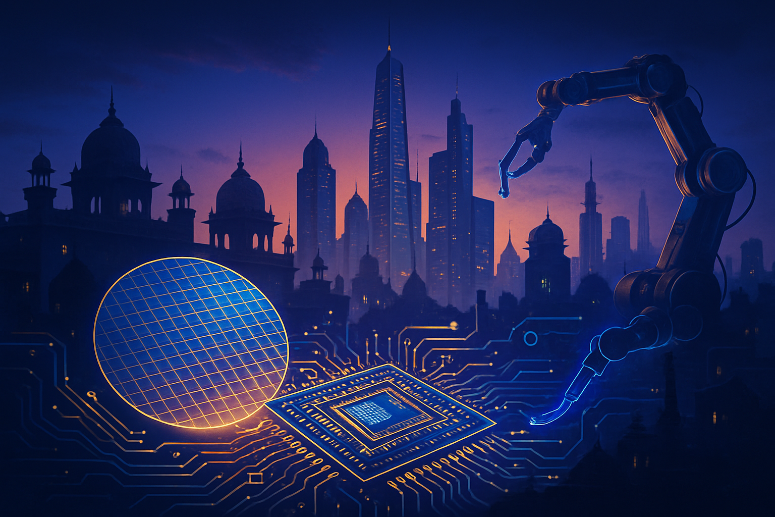
    In a relentless pursuit of ever-greater computing power, the semiconductor industry is undergoing a profound transformation, moving beyond the traditional two-dimensional scaling of transistors. Advanced packaging technologies, particularly 3D stacking and modular chiplet architectures, are emerging as the new frontier, enabling unprecedented levels of performance, power efficiency, and miniaturization critical for the burgeoning demands of artificial intelligence, high-performance computing, and the ubiquitous Internet of Things. These innovations are not just incremental improvements; they represent a fundamental shift in how chips are designed and manufactured, promising to unlock the next generation of intelligent devices and data centers.

    This paradigm shift comes as traditional Moore's Law, which predicted the doubling of transistors on a microchip every two years, faces increasing physical and economic limitations. By vertically integrating multiple dies and disaggregating complex systems into specialized chiplets, the industry is finding new avenues to overcome these challenges, fostering a new era of heterogeneous integration that is more flexible, powerful, and sustainable. The implications for technological advancement across every sector are immense, as these packaging breakthroughs pave the way for more compact, faster, and more energy-efficient silicon solutions.

    Engineering the Third Dimension: Unpacking 3D Stacking and Chiplet Architectures

    At the heart of this revolution are two interconnected yet distinct approaches: 3D stacking and chiplet architectures. 3D stacking, often referred to as 3D packaging or 3D integration, involves the vertical assembly of multiple semiconductor dies (chips) within a single package. This technique dramatically shortens the interconnect distances between components, a critical factor for boosting performance and reducing power consumption. Key enablers of 3D stacking include Through-Silicon Vias (TSVs) and hybrid bonding. TSVs are tiny, vertical electrical connections that pass directly through the silicon substrate, allowing stacked chips to communicate at high speeds with minimal latency. Hybrid bonding, an even more advanced technique, creates direct copper-to-copper interconnections between wafers or dies at pitches below 10 micrometers, offering superior density and lower parasitic capacitance than older microbump technologies. This is particularly vital for applications like High-Bandwidth Memory (HBM), where memory dies are stacked directly with processors to create high-throughput systems essential for AI accelerators and HPC.

    Chiplet architectures, on the other hand, involve breaking down a complex System-on-Chip (SoC) into smaller, specialized functional blocks—or "chiplets"—that are then interconnected on a single package. This modular approach allows each chiplet to be optimized for its specific function (e.g., CPU cores, GPU cores, I/O, memory controllers) and even fabricated using different, most suitable process nodes. The Universal Chiplet Interconnect Express (UCIe) standard is a crucial development in this space, providing an open die-to-die interconnect specification that defines the physical link, link-level behavior, and protocols for seamless communication between chiplets. The recent release of UCIe 3.0 in August 2025, which supports data rates up to 64 GT/s and includes enhancements like runtime recalibration for power efficiency, signifies a maturing ecosystem for modular chip design. This contrasts sharply with traditional monolithic chip design, where all functionalities are integrated onto a single, large die, leading to challenges in yield, cost, and design complexity as chips grow larger. The industry's initial reaction has been overwhelmingly positive, with major players aggressively investing in these technologies to maintain a competitive edge.

    Competitive Battlegrounds and Strategic Advantages

    The shift to advanced packaging technologies is creating new competitive battlegrounds and strategic advantages across the semiconductor industry. Foundry giants like TSMC (NYSE: TSM), Intel (NASDAQ: INTC), and Samsung (KRX: 005930) are at the forefront, heavily investing in their advanced packaging capabilities. TSMC, for instance, is a leader with its 3DFabric™ suite, including CoWoS® (Chip-on-Wafer-on-Substrate) and SoIC™ (System-on-Integrated-Chips), and is aggressively expanding CoWoS capacity to quadruple output by the end of 2025, reaching 130,000 wafers per month by 2026 to meet soaring AI demand. Intel is leveraging its Foveros (true 3D stacking with hybrid bonding) and EMIB (Embedded Multi-die Interconnect Bridge) technologies, while Samsung recently announced plans to restart a $7 billion advanced packaging factory investment driven by long-term AI semiconductor supply contracts.

    Chip designers like AMD (NASDAQ: AMD) and NVIDIA (NASDAQ: NVDA) are direct beneficiaries. AMD has been a pioneer in chiplet-based designs for its EPYC CPUs and Ryzen processors, including 3D V-Cache which utilizes 3D stacking for enhanced gaming and server performance, with new Ryzen 9000 X3D series chips expected in late 2025. NVIDIA, a dominant force in AI GPUs, heavily relies on HBM integrated through 3D stacking for its high-performance accelerators. The competitive implications are significant; companies that master these packaging technologies can offer superior performance-per-watt and more cost-effective solutions, potentially disrupting existing product lines and forcing competitors to accelerate their own packaging roadmaps. Packaging specialists like Amkor Technology and ASE (Advanced Semiconductor Engineering) are also expanding their capacities, with Amkor breaking ground on a new $7 billion advanced packaging and test campus in Arizona in October 2025 and ASE expanding its K18B factory. Even equipment manufacturers like ASML are adapting, with ASML introducing the Twinscan XT:260 lithography scanner in October 2025, specifically designed for advanced 3D packaging.

    Reshaping the AI Landscape and Beyond

    These advanced packaging technologies are not merely technical feats; they are fundamental enablers for the broader AI landscape and other critical technology trends. By providing unprecedented levels of integration and performance, they directly address the insatiable computational demands of modern AI models, from large language models to complex neural networks for computer vision and autonomous driving. The ability to integrate high-bandwidth memory directly with processing units through 3D stacking significantly reduces data bottlenecks, allowing AI accelerators to process vast datasets more efficiently. This directly translates to faster training times, more complex model architectures, and more responsive AI applications.

    The impacts extend far beyond AI, underpinning advancements in 5G/6G communications, edge computing, autonomous vehicles, and the Internet of Things (IoT). Smaller form factors enable more powerful and sophisticated devices at the edge, while increased power efficiency is crucial for battery-powered IoT devices and energy-conscious data centers. This marks a significant milestone comparable to the introduction of multi-core processors or the shift to FinFET transistors, as it fundamentally alters the scaling trajectory of computing. However, this progress is not without its concerns. Thermal management becomes a significant challenge with densely packed, vertically integrated chips, requiring innovative cooling solutions. Furthermore, the increased manufacturing complexity and associated costs of these advanced processes pose hurdles for wider adoption, requiring significant capital investment and expertise.

    The Horizon: What Comes Next

    Looking ahead, the trajectory for advanced packaging is one of continuous innovation and broader adoption. In the near term, we can expect to see further refinement of hybrid bonding techniques, pushing interconnect pitches even finer, and the continued maturation of the UCIe ecosystem, leading to a wider array of interoperable chiplets from different vendors. Experts predict that the integration of optical interconnects within packages will become more prevalent, offering even higher bandwidth and lower power consumption for inter-chiplet communication. The development of advanced thermal solutions, including liquid cooling directly within packages, will be critical to manage the heat generated by increasingly dense 3D stacks.

    Potential applications on the horizon are vast. Beyond current AI accelerators, we can anticipate highly customized, domain-specific architectures built from a diverse catalog of chiplets, tailored for specific tasks in healthcare, finance, and scientific research. Neuromorphic computing, which seeks to mimic the human brain's structure, could greatly benefit from the dense, low-latency interconnections offered by 3D stacking. Challenges remain in standardizing testing methodologies for complex multi-die packages and developing sophisticated design automation tools that can efficiently manage the design of heterogeneous systems. Industry experts predict a future where the "system-in-package" becomes the primary unit of innovation, rather than the monolithic chip, fostering a more collaborative and specialized semiconductor ecosystem.

    A New Era of Silicon Innovation

    In summary, advanced packaging technologies like 3D stacking and chiplets are not just incremental improvements but foundational shifts that are redefining the limits of semiconductor performance, power efficiency, and form factor. By enabling unprecedented levels of heterogeneous integration, these innovations are directly fueling the explosive growth of artificial intelligence and high-performance computing, while also providing crucial advancements for 5G/6G, autonomous systems, and the IoT. The competitive landscape is being reshaped, with major foundries and chip designers heavily investing to capitalize on these capabilities.

    While challenges such as thermal management and manufacturing complexity persist, the industry's rapid progress, evidenced by the maturation of standards like UCIe 3.0 and aggressive capacity expansions from key players, signals a robust commitment to this new paradigm. This development marks a significant chapter in AI history, moving beyond transistor scaling to architectural innovation at the packaging level. In the coming weeks and months, watch for further announcements regarding new chiplet designs, expanded production capacities, and the continued evolution of interconnect standards, all pointing towards a future where modularity and vertical integration are the keys to unlocking silicon's full potential.


    This content is intended for informational purposes only and represents analysis of current AI developments.

    TokenRing AI delivers enterprise-grade solutions for multi-agent AI workflow orchestration, AI-powered development tools, and seamless remote collaboration platforms.
    For more information, visit https://www.tokenring.ai/.

  • The AI Supercycle: Reshaping the Semiconductor Landscape and Driving Unprecedented Growth

    The AI Supercycle: Reshaping the Semiconductor Landscape and Driving Unprecedented Growth

    The global semiconductor market in late 2025 is in the throes of an unprecedented transformation, largely propelled by the relentless surge of Artificial Intelligence (AI). This "AI Supercycle" is not merely a cyclical uptick but a fundamental re-architecture of market dynamics, driving exponential demand for specialized chips and reshaping investment outlooks across the industry. While leading-edge foundries like Taiwan Semiconductor Manufacturing Company (NYSE: TSM) and NVIDIA Corporation (NASDAQ: NVDA) ride a wave of record profits, specialty foundries like Tower Semiconductor Ltd. (NASDAQ: TSEM) are strategically positioned to capitalize on the increasing demand for high-value analog and mature node solutions that underpin the AI infrastructure.

    The industry is projected for substantial expansion, with growth forecasts for 2025 ranging from 11% to 22.2% year-over-year, anticipating market values between $697 billion and $770 billion, and a trajectory to surpass $1 trillion by 2030. This growth, however, is bifurcated, with AI-focused segments booming while traditional markets experience a more gradual recovery. Investors are keenly watching the interplay of technological innovation, geopolitical pressures, and evolving supply chain strategies, all of which are influencing company valuations and long-term investment prospects.

    The Technical Core: Driving the AI Revolution from Silicon to Software

    Late 2025 marks a critical juncture defined by rapid advancements in process nodes, memory technologies, advanced packaging, and AI-driven design tools, all meticulously engineered to meet AI's insatiable computational demands. This period fundamentally differentiates itself from previous market cycles.

    The push for smaller, more efficient chips is accelerating with 3nm and 2nm manufacturing nodes at the forefront. TSMC has been in mass production of 3nm chips for three years and plans to expand its 3nm capacity by over 60% in 2025. More significantly, TSMC is on track for mass production of its 2nm chips (N2) in the second half of 2025, featuring nanosheet transistors for up to 15% speed improvement or 30% power reduction over N3E. Competitors like Intel Corporation (NASDAQ: INTC) are aggressively pursuing their Intel 18A process (equivalent to 1.8nm) for leadership in 2025, utilizing RibbonFET (GAA) transistors and PowerVia backside power delivery. Samsung Electronics Co., Ltd. (KRX: 005930) also aims to start production of 2nm-class chips in 2025. This transition to Gate-All-Around (GAA) transistors represents a significant architectural shift, enhancing efficiency and density.

    High-Bandwidth Memory (HBM), particularly HBM3e and the emerging HBM4, is indispensable for AI and High-Performance Computing (HPC) due to its ultra-fast, energy-efficient data transfer. Mass production of 12-layer HBM3e modules began in late 2024, offering significantly higher bandwidth (up to 1.2 TB/s per stack) for generative AI workloads. Micron Technology, Inc. (NASDAQ: MU) and SK hynix Inc. (KRX: 000660) are leading the charge, with HBM4 development accelerating for mass production by late 2025 or 2026, promising a ~20% increase in pricing. HBM revenue is projected to double from $17 billion in 2024 to $34 billion in 2025, playing an increasingly critical role in AI infrastructure and causing a "super cycle" in the broader memory market.

    Advanced packaging technologies such as Chip-on-Wafer-on-Substrate (CoWoS), System-on-Integrated-Chips (SoIC), and hybrid bonding are crucial for overcoming the limitations of traditional monolithic chip designs. TSMC is aggressively expanding its CoWoS capacity, aiming to double output in 2025 to 680,000 wafers, essential for high-performance AI accelerators. These techniques enable heterogeneous integration and 3D stacking, allowing more transistors in a smaller space and boosting computational power. NVIDIA’s Hopper H200 GPUs, for example, integrate six HBM stacks using advanced packaging, enabling interconnection speeds of up to 4.8 TB/s.

    Furthermore, AI-driven Electronic Design Automation (EDA) tools are profoundly transforming the semiconductor industry. AI automates repetitive tasks like layout optimization and place-and-route, reducing manual iterations and accelerating time-to-market. Tools like Synopsys, Inc.'s (NASDAQ: SNPS) DSO.ai have cut 5nm chip design timelines from months to weeks, a 75% reduction, while Synopsys.ai Copilot, with generative AI capabilities, has slashed verification times by 5X-10X. This symbiotic relationship, where AI not only demands powerful chips but also empowers their creation, is a defining characteristic of the current "AI Supercycle," distinguishing it from previous boom-bust cycles driven by broad-based demand for PCs or smartphones. Initial reactions from the AI research community and industry experts range from cautious optimism regarding the immense societal benefits to concerns about supply chain bottlenecks and the rapid acceleration of technological cycles.

    Corporate Chessboard: Beneficiaries, Challengers, and Strategic Advantages

    The "AI Supercycle" has created a highly competitive and bifurcated landscape within the semiconductor industry, benefiting companies with strong AI exposure while posing unique challenges for others.

    NVIDIA (NASDAQ: NVDA) remains the undisputed dominant force, with its data center segment driving a 94% year-over-year revenue increase in Q3 FY25. Its Q4 FY25 revenue guidance of $37.5 billion, fueled by strong demand for Hopper/Blackwell GPUs, solidifies its position as a top investment pick. Similarly, TSMC (NYSE: TSM), as the world's largest contract chipmaker, reported record Q3 2025 results, with profits surging 39% year-over-year and revenue increasing 30.3% to $33.1 billion, largely due to soaring AI chip demand. TSMC’s market valuation surpassed $1 trillion in July 2025, and its stock price has risen nearly 48% year-to-date. Its advanced node capacity is sold out for years, primarily due to AI demand.

    Advanced Micro Devices, Inc. (NASDAQ: AMD) is actively expanding its presence in AI and data center partnerships, but its high P/E ratio of 102 suggests much of its rapid growth potential is already factored into its valuation. Intel (NASDAQ: INTC) has shown improved execution in Q3 2025, with AI accelerating demand across its portfolio. Its stock surged approximately 84% year-to-date, buoyed by government investments and strategic partnerships, including a $5 billion deal with NVIDIA. However, its foundry division still operates at a loss, and it faces structural challenges. Broadcom Inc. (NASDAQ: AVGO) also demonstrated strong performance, with AI-specific revenue surging 63% to $5.2 billion in Q3 FY25, including a reported $10 billion AI order for FY26.

    Tower Semiconductor (NASDAQ: TSEM) has carved a strategic niche as a specialized foundry focusing on high-value analog and mixed-signal solutions, distinguishing itself from the leading-edge digital foundries. For Q2 2025, Tower reported revenues of $372 million, up 6% year-over-year, with a net profit of $47 million. Its Q3 2025 revenue guidance of $395 million projects a 7% year-over-year increase, driven by strong momentum in its RF infrastructure business, particularly from data centers and AI expansions, where it holds a number one market share position. Significant growth was also noted in Silicon Photonics and RF Mobile markets. Tower's stock reached a new 52-week high of $77.97 in late October 2025, reflecting a 67.74% increase over the past year. Its strategic advantages include specialized process platforms (SiGe, BiCMOS, RF CMOS, power management), leadership in RF and photonics for AI data centers and 5G/6G, and a global, flexible manufacturing network.

    While Tower Semiconductor does not compete directly with TSMC or Samsung Foundry in the most advanced digital logic nodes (sub-7nm), it thrives in complementary markets. Its primary competitors in the specialized and mature node segments include United Microelectronics Corporation (NYSE: UMC) and GlobalFoundries Inc. (NASDAQ: GFS). Tower’s deep expertise in RF, power management, and analog solutions positions it favorably to capitalize on the increasing demand for high-performance analog and RF front-end components essential for AI and cloud computing infrastructure. The AI Supercycle, while primarily driven by advanced digital chips, significantly benefits Tower through the need for high-speed optical communications and robust power management within AI data centers. Furthermore, sustained demand for mature nodes in automotive, industrial, and consumer electronics, along with anticipated shortages of mature node chips (40nm and above) for the automotive industry, provides a stable and growing market for Tower's offerings.

    Wider Significance: A Foundational Shift for AI and Global Tech

    The semiconductor industry's performance in late 2025, defined by the "AI Supercycle," represents a foundational shift with profound implications for the broader AI landscape and global technology. This era is not merely about faster chips; it's about a symbiotic relationship where AI both demands ever more powerful semiconductors and, paradoxically, empowers their very creation through AI-driven design and manufacturing.

    Chip supply and innovation directly dictate the pace of AI development, deployment, and accessibility. The availability of specialized AI chips (GPUs, TPUs, ASICs), High-Bandwidth Memory (HBM), and advanced packaging techniques like 3D stacking are critical enablers for large language models, autonomous systems, and advanced scientific AI. AI-powered Electronic Design Automation (EDA) tools are compressing chip design cycles by automating complex tasks and optimizing performance, power, and area (PPA), accelerating innovation from months to weeks. This efficient and cost-effective chip production translates into cheaper, more powerful, and more energy-efficient chips for cloud infrastructure and edge AI deployments, making AI solutions more accessible across various industries.

    However, this transformative period comes with significant concerns. Market concentration is a major issue, with NVIDIA dominating AI chips and TSMC being a critical linchpin for advanced manufacturing (90% of the world's most advanced logic chips). The Dutch firm ASML Holding N.V. (NASDAQ: ASML) holds a near-monopoly on extreme ultraviolet (EUV) lithography machines, indispensable for advanced chip production. This concentration risks centralizing AI power among a few tech giants and creating high barriers for new entrants.

    Geopolitical tensions have also transformed semiconductors into strategic assets. The US-China rivalry over advanced chip access, characterized by export controls and efforts towards self-sufficiency, has fragmented the global supply chain. Initiatives like the US CHIPS Act aim to bolster domestic production, but the industry is moving from globalization to "technonationalism," with countries investing heavily to reduce dependence. This creates supply chain vulnerabilities, cost uncertainties, and trade barriers. Furthermore, an acute and widening global shortage of skilled professionals—from fab labor to AI and advanced packaging engineers—threatens to slow innovation.

    The environmental impact is another growing concern. The rapid deployment of AI comes with a significant energy and resource cost. Data centers, the backbone of AI, are facing an unprecedented surge in energy demand, primarily from power-hungry AI accelerators. TechInsights forecasts a staggering 300% increase in CO2 emissions from AI accelerators alone between 2025 and 2029. Manufacturing high-end AI chips consumes substantial electricity and water, often concentrated in regions reliant on fossil fuels. This era is defined by an unprecedented demand for specialized, high-performance computing, driving innovation at a pace that could lead to widespread societal and economic restructuring on a scale even greater than the PC or internet revolutions.

    The Horizon: Future Developments and Enduring Challenges

    Looking ahead, the semiconductor industry is poised for continued rapid evolution, driven by the escalating demands of AI. Near-term (2025-2030) developments will focus on refining AI models for hyper-personalized manufacturing, boosting data center AI semiconductor revenue, and integrating AI into PCs and edge devices. The long-term outlook (beyond 2030) anticipates revolutionary changes with new computing paradigms.

    The evolution of AI chips will continue to emphasize specialized hardware like GPUs and ASICs, with increasing focus on energy efficiency for both cloud and edge applications. On-chip optical communication using silicon photonics, continued memory innovation (e.g., HBM and GDDR7), and backside power delivery are predicted key innovations. Beyond 2030, neuromorphic computing, inspired by the human brain, promises energy-efficient processing for real-time perception and pattern recognition in autonomous vehicles, robots, and wearables. Quantum computing, while still 5-10 years from achieving quantum advantage, is already influencing semiconductor roadmaps, driving innovation in materials and fabrication techniques for atomic-scale precision and cryogenic operation.

    Advanced manufacturing techniques will increasingly rely on AI for automation, optimization, and defect detection. Advanced packaging (2.5D and 3D stacking, hybrid bonding) will become even more crucial for heterogeneous integration, improving performance and power efficiency of complex AI systems. The search for new materials will intensify as silicon reaches its limits. Wide-bandbandgap semiconductors like Gallium Nitride (GaN) and Silicon Carbide (SiC) are outperforming silicon in high-frequency and high-power applications (5G, EVs, data centers). Two-dimensional materials like graphene and molybdenum disulfide (MoS₂) offer potential for ultra-thin, highly conductive, and flexible transistors.

    However, significant challenges persist. Manufacturing costs for advanced fabs remain astronomical, requiring multi-billion dollar investments and cutting-edge skills. The global talent shortage in semiconductor design and manufacturing is projected to exceed 1 million workers by 2030, threatening to slow innovation. Geopolitical risks, particularly the dependence on Taiwan for advanced logic chips and the US-China trade tensions, continue to fragment the supply chain, necessitating "friend-shoring" strategies and diversification of manufacturing bases.

    Experts predict the total semiconductor market will surpass $1 trillion by 2030, growing at 7%-9% annually post-2025, primarily driven by AI, electric vehicles, and consumer electronics replacement cycles. Companies like Tower Semiconductor, with their focus on high-value analog and specialized process technologies, will play a vital role in providing the foundational components necessary for this AI-driven future, particularly in critical areas like RF, power management, and Silicon Photonics. By diversifying manufacturing facilities and investing in talent development, specialty foundries can contribute to supply chain resilience and maintain competitiveness in this rapidly evolving landscape.

    Comprehensive Wrap-up: A New Era of Silicon and AI

    The semiconductor industry in late 2025 is undergoing an unprecedented transformation, driven by the "AI Supercycle." This is not just a period of growth but a fundamental redefinition of how chips are designed, manufactured, and utilized, with profound implications for technology and society. Key takeaways include the explosive demand for AI chips, the critical role of advanced process nodes (3nm, 2nm), HBM, and advanced packaging, and the symbiotic relationship where AI itself is enhancing chip manufacturing efficiency.

    This development holds immense significance in AI history, marking a departure from previous tech revolutions. Unlike the PC or internet booms, where semiconductors primarily enabled new technologies, the AI era sees AI both demanding increasingly powerful chips and * empowering* their creation. This dual nature positions AI as both a driver of unprecedented technological advancement and a source of significant challenges, including market concentration, geopolitical tensions, and environmental concerns stemming from energy consumption and e-waste.

    In the long term, the industry is headed towards specialized AI architectures like neuromorphic computing, the exploration of quantum computing, and the widespread deployment of advanced edge AI. The transition to new materials beyond silicon, such as GaN and SiC, will be crucial for future performance gains. Companies like Tower Semiconductor, with their focus on high-value analog and specialized process technologies, will play a vital role in providing the foundational components necessary for this AI-driven future, particularly in critical areas like RF, power management, and Silicon Photonics.

    What to watch for in the coming weeks and months includes further announcements on 2nm chip production, the acceleration of HBM4 development, increased investments in advanced packaging capacity, and the rollout of new AI-driven EDA tools. Geopolitical developments, especially regarding trade policies and domestic manufacturing incentives, will continue to shape supply chain strategies. Investors will be closely monitoring the financial performance of AI-centric companies and the strategic adaptations of specialty foundries as the "AI Supercycle" continues to reshape the global technology landscape.


    This content is intended for informational purposes only and represents analysis of current AI developments.

    TokenRing AI delivers enterprise-grade solutions for multi-agent AI workflow orchestration, AI-powered development tools, and seamless remote collaboration platforms.
    For more information, visit https://www.tokenring.ai/.

  • Fed’s October Rate Cut Ignites Tech Sector Optimism Amidst Economic Shifts

    Fed’s October Rate Cut Ignites Tech Sector Optimism Amidst Economic Shifts

    Washington D.C., October 24, 2025 – As the Federal Reserve's Open Market Committee (FOMC) concludes its critical October 28-29 meeting, the overwhelming consensus among economists and market participants points to a widely anticipated interest rate cut. This move, expected to be a quarter-point (25 basis points) reduction in the federal funds rate, marks the second consecutive cut this autumn, signaling a significant pivot in monetary policy designed to bolster a softening labor market. For the technology sector, this easing of financial conditions is largely viewed as a potent catalyst, promising lower borrowing costs, enhanced investment opportunities, and a renewed surge in investor confidence, particularly in the burgeoning field of artificial intelligence.

    The immediate significance of this decision cannot be overstated for an industry heavily reliant on capital for innovation and growth. While inflation persists above the Fed's 2% target, the central bank's focus has clearly shifted towards mitigating risks to employment. This strategic recalibration by the Fed is poised to inject fresh liquidity and optimism into tech markets, which have already demonstrated remarkable resilience and growth, driven in no small part by the transformative power of AI.

    Monetary Policy's New Trajectory: Fueling Tech's Future

    The projected rate cut, which would place the federal funds rate target range between 3.75% and 4%—a level not seen since late 2022—is a direct response to a weakening labor market. Recent data from the Bureau of Labor Statistics revealed a substantial downward revision of nearly a million jobs created between April 2024 and March 2025, alongside a significant dip in consumer confidence regarding employment prospects. While the Consumer Price Index (CPI) in September registered 3% year-over-year, slightly above target but below forecasts, the more closely watched "core" inflation also showed a modest decline, offering the Fed the necessary latitude to prioritize economic growth and employment.

    This monetary easing differs significantly from previous periods of aggressive rate hikes, where the primary objective was to curb soaring inflation. The current environment sees the Fed navigating a more complex landscape, balancing persistent inflation with clear signs of economic deceleration, particularly in employment. By reducing borrowing costs, the Fed aims to stimulate corporate investment, encourage hiring, and prevent a deeper economic downturn. This approach provides a crucial lifeline for growth-oriented sectors like technology, which often rely on accessible capital for research and development, market expansion, and talent acquisition.

    Initial reactions from the AI research community and industry experts are cautiously optimistic. Lower interest rates are expected to directly reduce the cost of capital for tech companies, improving their profitability and allowing for greater reinvestment into cutting-edge AI projects. This financial tailwind could accelerate the pace of innovation, enabling companies to push the boundaries of machine learning, natural language processing, and advanced robotics. Experts note that while the broader economic picture remains nuanced, the Fed's proactive stance in supporting growth is a net positive for an industry that thrives on capital availability and future-oriented investments.

    Corporate Beneficiaries and Competitive Dynamics in a Looser Credit Environment

    The anticipated rate cut is set to create a ripple effect across the technology sector, significantly benefiting companies at various stages of maturity. Growth-oriented startups and mid-sized tech firms, which often rely on venture capital and debt financing to scale operations and fund ambitious AI initiatives, will find capital more accessible and less expensive. This could lead to a resurgence in fundraising rounds, initial public offerings (IPOs), and mergers and acquisitions (M&A) activities, providing a much-needed boost to the innovation ecosystem.

    Established tech giants such as Apple (NASDAQ: AAPL), Microsoft (NASDAQ: MSFT), Alphabet (NASDAQ: GOOGL), and Amazon (NASDAQ: AMZN) also stand to gain. While these companies often have robust balance sheets, lower borrowing costs can enhance their ability to finance large-scale infrastructure projects, invest in strategic AI acquisitions, and optimize their capital structures. For example, companies heavily investing in data centers and specialized hardware for AI training, like Microsoft and Alphabet, could see reduced costs associated with expanding their computational capabilities. This competitive advantage allows them to further solidify their market positioning and accelerate their AI development roadmaps.

    The competitive implications are profound. Companies with strong AI portfolios and clear growth trajectories are likely to attract even more investor interest, potentially leading to higher valuations. This environment could exacerbate the divide between well-funded, innovative players and those struggling to secure capital, potentially leading to consolidation within certain tech sub-sectors. Furthermore, lower rates might encourage tech giants to acquire promising AI startups, integrating their technologies and talent to gain an edge. This could disrupt existing product roadmaps by accelerating the deployment of advanced AI features across various platforms and services, from cloud computing to consumer electronics.

    Broadening Horizons: AI's Role in a Shifting Economic Landscape

    The Fed's pivot towards rate cuts fits squarely into a broader economic landscape characterized by a delicate balance between inflation management and growth stimulation. For the AI industry, this decision arrives at a pivotal moment, further fueling an investment boom that has already seen unprecedented capital flowing into artificial intelligence. The accessibility of cheaper capital could accelerate the development and deployment of AI across various sectors, from healthcare and finance to manufacturing and logistics, driving productivity gains and fostering new markets.

    However, the wider significance also brings potential concerns. While lower rates are generally positive for growth, they could also contribute to asset price inflation, particularly in highly valued tech stocks. Some experts draw parallels to previous periods of market exuberance, cautioning against the potential for overvaluation in certain segments of the tech market, especially for U.S. tech mega-caps. The continued stock gains for these companies will depend heavily on their ability to meet increasingly elevated profit expectations, a challenge even with reduced borrowing costs.

    Compared to previous AI milestones, where breakthroughs were often driven by scientific advancements, the current environment sees economic policy playing a direct and significant role in shaping the industry's trajectory. The Fed's actions underscore the growing interdependence between macroeconomic conditions and technological innovation. This period could be viewed as a critical juncture where financial incentives align with technological potential, potentially accelerating the mainstream adoption and commercialization of AI solutions on an unprecedented scale.

    The Road Ahead: Anticipating AI's Next Evolution

    Looking ahead, the near-term developments in the tech sector are expected to be marked by a surge in investment and strategic maneuvering. Companies are likely to leverage the lower cost of capital to double down on AI research and development, expand their cloud infrastructure, and invest in talent acquisition. We can anticipate an increase in strategic partnerships and collaborations aimed at accelerating AI innovation and bringing new applications to market. The focus will be on refining existing AI models, improving efficiency, and developing more specialized AI solutions for various industries.

    In the long term, the sustained availability of capital at lower rates could foster a new wave of disruptive AI startups, challenging established players and driving further innovation. Potential applications and use cases on the horizon include more sophisticated AI-powered automation in manufacturing, advanced diagnostic tools in healthcare, highly personalized educational platforms, and more intuitive human-computer interfaces. The focus will shift towards ethical AI development, robust data governance, and ensuring the equitable distribution of AI's benefits.

    However, challenges remain. The tech sector will need to address concerns around AI's societal impact, including job displacement, algorithmic bias, and data privacy. Regulatory frameworks will continue to evolve, and companies will need to navigate an increasingly complex legal and ethical landscape. Experts predict that the next phase of AI development will not only be about technological breakthroughs but also about responsible deployment and integration into society. What happens next will largely depend on how effectively tech companies can balance innovation with ethical considerations and how regulatory bodies respond to the rapid pace of AI advancement.

    A New Chapter for Tech and AI: Navigating the Future

    The October 2025 Federal Reserve meeting, with its widely anticipated interest rate cut, marks a significant turning point for the technology sector and the broader economy. The key takeaway is a clear signal from the Fed that it is prioritizing economic growth and employment, even as it continues to monitor inflation. For tech, this translates into a more favorable financial environment, potentially fueling a renewed surge in innovation, investment, and market expansion, particularly within the AI landscape.

    This development holds considerable significance in AI history, as it underscores how macroeconomic policies can directly influence the speed and direction of technological progress. The availability of cheaper capital is not just an economic boon; it's an accelerator for scientific and engineering endeavors, enabling the ambitious projects that define the frontier of AI. As companies like NVIDIA (NASDAQ: NVDA) and Advanced Micro Devices (NASDAQ: AMD) continue to build the foundational hardware for AI, and software companies develop ever more sophisticated models, the financial environment will play a critical role in how quickly these innovations reach the market.

    In the coming weeks and months, all eyes will be on how tech companies leverage this new financial landscape. We should watch for increased venture capital activity, a potential uptick in IPOs, and strategic M&A deals. Furthermore, observing how major tech players allocate their newfound financial flexibility towards AI research, ethical development, and market expansion will be crucial. The interplay between monetary policy and technological advancement is creating a dynamic and exciting, albeit challenging, future for artificial intelligence.


    This content is intended for informational purposes only and represents analysis of current AI developments.

    TokenRing AI delivers enterprise-grade solutions for multi-agent AI workflow orchestration, AI-powered development tools, and seamless remote collaboration platforms.
    For more information, visit https://www.tokenring.ai/.

  • Quantum Leap: U.S. Government Fuels Quantum Computing Race Amidst Breakthroughs and Emerging Investment Avenues

    Quantum Leap: U.S. Government Fuels Quantum Computing Race Amidst Breakthroughs and Emerging Investment Avenues

    October 23, 2025 – The world of computing is experiencing a seismic shift, as quantum technology rapidly accelerates from theoretical promise to tangible reality. Late 2025 marks a pivotal moment, characterized by groundbreaking advancements in quantum hardware and software, a fervent push for practical applications, and an unprecedented surge in U.S. government interest, including potential direct equity investments in leading quantum firms. This confluence of innovation and strategic backing is not only redefining the computational landscape but also opening new, diversified avenues for investors to participate in the burgeoning quantum economy.

    The immediate significance of these developments cannot be overstated. With quantum computers demonstrating verifiable advantages over classical supercomputers in specific tasks, the race for quantum supremacy has intensified, becoming a critical battleground for national security and economic leadership. The U.S. government's proactive stance, moving beyond traditional grants to consider direct stakes in private companies, underscores the strategic importance of this technology, signaling a robust commitment to securing a dominant position in the global quantum arms race.

    The Dawn of Practical Quantum Advantage: A Technical Deep Dive

    The technical advancements in quantum computing as of late 2025 are nothing short of revolutionary, pushing the boundaries of what was once considered science fiction. A key highlight is Google Quantum AI's demonstration of "verifiable quantum advantage" with its 65-qubit Willow chip. This was achieved by running a specialized "Quantum Echoes" algorithm, which models atomic interactions, an astonishing 13,000 times faster than the Frontier supercomputer. Unlike previous demonstrations, the verifiability of these results signifies a critical step towards practical, real-world applications, offering a blueprint for solving problems in fields like medicine and materials science that are currently intractable for classical machines.

    Processor architectures are evolving at an unprecedented pace. IBM (NYSE: IBM) has deployed upgraded Heron processors within its modular Quantum System Two, designed for scalable quantum computation, while its 1,121-qubit Condor processor, launched in late 2024, incorporates advanced error correction. Microsoft (NASDAQ: MSFT) made waves with its "Majorana 1" quantum processing unit in February 2025, leveraging topological qubits for inherent stability and a potential path to scale to millions of qubits on a single chip. Rigetti Computing (NASDAQ: RGTI) has made its 36-qubit multi-chip quantum computer generally available and aims for a 100-qubit system with 99.5% fidelity by year-end. These innovations represent a departure from earlier efforts, focusing not just on raw qubit count but on stability, error reduction, and modularity.

    Hybrid quantum-classical systems are emerging as the pragmatic bridge to near-term utility. NVIDIA (NASDAQ: NVDA) and Quantum Machines debuted DGX Quantum in March 2025, a tightly integrated system combining NVIDIA's Grace Hopper Superchip with Quantum Machines' OPX1000, achieving sub-4-microsecond latency between GPU and QPU. This ultra-fast communication is crucial for real-time quantum error correction and advanced adaptive circuits, making complex hybrid algorithms feasible within the fleeting coherence times of qubits. Amazon (NASDAQ: AMZN) has also deepened its integration between its Braket quantum cloud and NVIDIA's CUDA-Q tools, streamlining classical-quantum interaction.

    Crucially, significant progress has been made in quantum error correction and qubit stability. Google's Willow chip demonstrated that logical qubits could last more than twice as long as individual ones, with a significantly reduced error rate, a foundational step toward fault-tolerant quantum computing. The Defense Advanced Research Projects Agency (DARPA) launched the US2QC program, with Microsoft and SCI Quantum developing architectures for automatic detection and correction of quantum errors. These advancements address the inherent fragility of qubits, a major hurdle in scaling quantum systems, and are met with considerable optimism by the quantum research community, who see the shift to logical qubits as a "game-changer" on the path to practical, large-scale quantum computers.

    Corporate Beneficiaries and Competitive Implications

    The accelerating pace of quantum computing and robust government backing are creating a dynamic environment for quantum companies, tech giants, and startups, shaping new competitive landscapes and market positioning. Companies poised to benefit significantly include dedicated quantum computing firms, as well as established tech giants with substantial R&D investments.

    Among the pure-play quantum companies, IonQ (NYSE: IONQ) stands out as a leader in trapped-ion quantum computers, actively pursuing federal government contracts and achieving new performance milestones. Its integration with major cloud services like Amazon Braket and its own IonQ Quantum Cloud positions it strongly. Rigetti Computing (NASDAQ: RGTI), a full-stack quantum computing company, continues to advance its superconducting processors and has secured deals with the U.S. Air Force, highlighting its strategic importance. D-Wave Quantum (NYSE: QBTS), a pioneer in quantum annealing, is expanding its market reach, including a partnership for U.S. government IT distribution. These companies are not only benefiting from technological breakthroughs but also from the "seal of approval" and risk mitigation offered by potential government investment, leading to increased investor confidence and surging stock prices despite current unprofitability.

    Tech giants are strategically positioning themselves through vertical integration and ecosystem development. IBM (NYSE: IBM), with its ambitious roadmap to over 4,000 qubits by 2025 and a focus on quantum-centric supercomputing, aims to make quantum performance measurable in real-world problems across various industries. Google (NASDAQ: GOOGL), through Google Quantum AI, is doubling down on quantum-classical hybrid systems for "utterly impossible" problems in drug design and clean energy, leveraging its verifiable quantum advantage. Microsoft (NASDAQ: MSFT) is heavily invested in the high-risk, high-reward path of topological qubits with its Majorana 1 chip, while its Azure Quantum platform integrates hardware from partners like Quantinuum and Atom Computing. Amazon (NASDAQ: AMZN), via AWS Braket, provides on-demand access to diverse quantum hardware, lowering entry barriers for enterprises and recently unveiled Ocelot, its first proprietary quantum chip.

    The competitive implications are profound. The U.S. government's direct investment signals an intensifying global race for quantum supremacy, compelling increased R&D spending and faster innovation. Hybridization and ecosystem development are becoming crucial differentiators, with companies that can effectively bridge the quantum-classical divide gaining a significant competitive edge. This intense competition also extends to talent acquisition, with a growing demand for specialized quantum physicists and engineers. Potential disruptions to existing products and services span cybersecurity, drug discovery, financial modeling, logistics, and AI/ML, as quantum computers promise to revolutionize these fields with unprecedented computational power. Market positioning is increasingly defined by early adoption, strategic partnerships, and a focus on demonstrating "practical advantage" in near-term applications, rather than solely long-term fault-tolerant systems.

    Wider Significance: A Paradigm Shift in the AI Landscape

    The advancements in quantum computing and the U.S. government's robust interest in late 2025 represent a profound shift with wider significance across the technological landscape, particularly for artificial intelligence. This is not merely an incremental improvement but a potential paradigm shift, akin to previous monumental breakthroughs in computing.

    Quantum computing is poised to become a strategic accelerator for AI, creating a powerful synergy. Quantum computers can significantly accelerate the training of large AI models, reducing training times from months to days by processing exponentially larger datasets and solving optimization problems faster. This capability extends to enhancing generative AI for tasks like molecule design and synthetic data generation, and addressing complex problem-solving in logistics and drug discovery. The relationship is bidirectional, with AI techniques being applied to optimize quantum circuit design and mitigate errors in noisy quantum systems, thereby improving the reliability and scalability of quantum technologies. This means quantum machine learning (QML) is emerging as a field that could handle high-dimensional or uncertain problems more effectively than classical systems, potentially leading to breakthroughs in optimization, image recognition, and cybersecurity.

    However, this transformative potential comes with significant concerns. The most pressing is the cybersecurity threat posed by fault-tolerant quantum computers, which could break widely used cryptographic systems through algorithms like Shor's. This necessitates an urgent and complex transition to post-quantum cryptography (PQC) to safeguard sensitive government information, financial transactions, and personal data. Ethical dilemmas and governance challenges also loom large, as the immense processing power could be misused for intrusive surveillance or manipulation. The high cost and specialized nature of quantum computing also raise concerns about exacerbating the digital divide and job displacement in certain sectors.

    Compared to previous AI milestones, quantum computing represents a fundamental shift in how computers process information, rather than just an advancement in what classical computers can do. While past AI breakthroughs, such as deep learning, pushed the boundaries within classical computing frameworks, quantum computing can tackle problems inherently suited to quantum mechanics, unlocking capabilities that classical AI simply cannot achieve on its own. It's a new computational paradigm that promises to accelerate and enhance existing AI, while also opening entirely new frontiers for scientific discovery and technological innovation. The verifiable quantum advantage demonstrations in late 2025 mark the beginning of quantum computers solving problems genuinely beyond classical means, a turning point in tech history.

    The Horizon: Future Developments and Challenges

    Looking ahead, the trajectory of quantum computing is marked by accelerating developments, with both near-term and long-term milestones on the horizon. Experts predict a future where quantum technology becomes an indispensable tool for solving humanity's most complex challenges.

    In the near-term (1-3 years), the focus will be on refining existing technologies and scaling hybrid quantum-classical systems. We can expect to see further advancements in quantum error mitigation, with logical qubits increasingly demonstrating superior error rates compared to physical qubits. Hardware will continue to evolve, with companies like Pasqal aiming for 10,000-qubit systems with scalable logical qubits by 2026. Early commercial applications will emerge at scale in sectors like pharmaceuticals, logistics, and financial services, demonstrating tangible returns on investment from specialized "Noisy Intermediate-Scale Quantum" (NISQ) devices. The emergence of diverse qubit technologies, including diamond-based systems for room-temperature operation, will also gain traction.

    The long-term (5-10+ years) vision centers on achieving Fault-Tolerant Quantum Computing (FTQC) and widespread practical applications. This will require millions of high-quality physical qubits to create stable logical qubits capable of running complex, error-free computations. IBM targets a fault-tolerant quantum computer by 2029 and useful scale by 2033. Google aims for a useful, error-corrected quantum computer by 2029. Beyond individual machines, the development of a quantum internet is anticipated to become a significant industry by 2030, enabling ultra-secure communications. Potential applications will revolutionize drug discovery, materials science, finance, logistics, and AI, by simulating molecular structures with unprecedented accuracy, optimizing complex processes, and supercharging AI algorithms.

    Despite the immense promise, significant challenges remain. Qubit fragility and decoherence continue to be a primary technical obstacle, requiring sophisticated error correction techniques. Scalability to hundreds or thousands of qubits while maintaining high coherence and low error rates is crucial. Hardware development faces hurdles in creating stable, high-quality qubits and control electronics, especially for systems that can operate outside extreme cryogenic environments. The software maturity and algorithm development still lag, and there's a significant skills gap in professionals trained in quantum mechanics. Addressing these challenges will require continued R&D investment, international collaboration, and a concerted effort to build a robust quantum workforce.

    Wrap-Up: A New Era of Computational Power

    The late 2025 landscape of quantum computing signifies a momentous turning point in technological history. The verifiable quantum advantage demonstrated by Google, coupled with the U.S. government's unprecedented interest and potential direct investments, underscores the strategic importance and accelerating maturity of this field. This era is characterized by a shift from purely theoretical exploration to tangible breakthroughs, particularly in hybrid quantum-classical systems and advancements in error correction and logical qubits.

    This development holds immense significance, comparable to the advent of the classical computer or the internet. It promises to unlock new frontiers in scientific research, reshape global economies through unprecedented optimization capabilities, and supercharge artificial intelligence. While the immediate threat to current encryption standards necessitates a rapid transition to post-quantum cryptography, quantum computing also offers the promise of ultra-secure communications. The long-term impact will be transformative, with quantum computers working in tandem with classical systems to solve problems currently beyond human reach, driving innovation across every sector.

    In the coming weeks and months, key areas to watch include the legislative progress on the reauthorization of the National Quantum Initiative Act, further details on U.S. government direct equity investments in quantum companies, and additional verifiable demonstrations of quantum advantage in commercially relevant problems. Continued advancements in error correction and logical qubits will be critical, as will the evolution of hybrid system architectures and the adoption of post-quantum cryptography standards.

    Investment Opportunities through ETFs

    For investors seeking exposure to this burgeoning sector, Exchange-Traded Funds (ETFs) offer a diversified approach to mitigate the risks associated with individual, often volatile, pure-play quantum stocks. As of late 2025, several ETFs provide access to the quantum computing theme:

    • Defiance Quantum ETF (NASDAQ: QTUM): This ETF provides diversified exposure to companies involved in quantum computing and machine learning, holding a basket of approximately 80 stocks, including tech giants like IBM, Alphabet (NASDAQ: GOOGL), and Microsoft (NASDAQ: MSFT), alongside pure-play quantum startups such as IonQ (NYSE: IONQ). It boasts nearly $2 billion in assets under management and an expense ratio of 0.40%.
    • VanEck Quantum Computing UCITS ETF (Europe – IE0007Y8Y157 / Ticker QNTM): Launched in May 2025, this is Europe's first and only ETF exclusively dedicated to quantum computing, tracking the MarketVector Global Quantum Leaders index. It has approximately €250 million in AUM and an expense ratio of 0.49% to 0.55%.
    • Spear Alpha ETF (NASDAQ: SPRX): An actively managed ETF with a concentrated portfolio, SPRX includes companies poised to benefit from quantum tech developments in related areas like AI. It has made significant allocations to pure-play quantum companies like Rigetti Computing (NASDAQ: RGTI) and IonQ (NYSE: IONQ), with an expense ratio of 0.75%.
    • Invesco Dorsey Wright Technology Momentum ETF (NASDAQ: PTF): This ETF offers indirect exposure by focusing on momentum-driven stocks within the broader information technology sector, including quantum companies if they exhibit strong price momentum. As of mid-September 2025, it held a position in Quantum Computing Inc. (NASDAQ: QUBT).

    Additionally, BlackRock is reportedly preparing an iShares Quantum Computing UCITS ETF in Europe, signaling increasing interest from major asset managers. These ETFs allow investors to participate in the "quantum gold rush" with a diversified portfolio, capitalizing on the long-term growth potential of this transformative technology.


    This content is intended for informational purposes only and represents analysis of current AI developments.

    TokenRing AI delivers enterprise-grade solutions for multi-agent AI workflow orchestration, AI-powered development tools, and seamless remote collaboration platforms.
    For more information, visit https://www.tokenring.ai/.

  • AI Supercharges Semiconductor Manufacturing: A New Era of Efficiency and Innovation Dawns

    AI Supercharges Semiconductor Manufacturing: A New Era of Efficiency and Innovation Dawns

    The semiconductor industry, the bedrock of the modern digital economy, is undergoing a profound transformation driven by the integration of artificial intelligence (AI) and machine learning (ML). As of October 2025, these advanced technologies are no longer just supplementary tools but have become foundational pillars, enabling unprecedented levels of efficiency, precision, and speed across the entire chip lifecycle. This paradigm shift is critical for addressing the escalating complexity of chip design and manufacturing, as well as the insatiable global demand for increasingly powerful and specialized semiconductors that fuel everything from cloud computing to edge AI devices.

    AI's immediate significance in semiconductor manufacturing lies in its ability to optimize intricate processes, predict potential failures, and accelerate innovation at a scale previously unimaginable. From enhancing yield rates in high-volume fabrication plants to dramatically compressing chip design cycles, AI is proving indispensable. This technological leap promises not only substantial cost reductions and faster time-to-market for new products but also ensures the production of higher quality, more reliable chips, cementing AI's role as the primary catalyst for the industry's evolution.

    The Algorithmic Forge: Technical Deep Dive into AI's Manufacturing Revolution

    The technical advancements brought by AI into semiconductor manufacturing are multifaceted and deeply impactful. At the forefront are sophisticated AI-powered solutions for yield optimization and process control. Companies like Lam Research (NASDAQ: LRCX) have introduced tools, such as their Fabtex™ Yield Optimizer, which leverage virtual silicon digital twins. These digital replicas, combined with real-time factory data, allow AI algorithms to analyze billions of data points, identify subtle process variations, and recommend real-time adjustments to parameters like temperature, pressure, and chemical composition. This proactive approach can reduce yield detraction by up to 30%, systematically targeting and mitigating yield-limiting mechanisms that previously required extensive manual analysis and trial-and-error.

    Beyond process control, advanced defect detection and quality control have seen revolutionary improvements. Traditional human inspection, often prone to error and limited by speed, is being replaced by AI-driven automated optical inspection (AOI) systems. These systems, utilizing deep learning and computer vision, can detect microscopic defects, cracks, and irregularities on wafers and chips with unparalleled speed and accuracy. Crucially, these AI models can identify novel or unknown defects, adapting to new challenges as manufacturing processes evolve or new materials are introduced, ensuring only the highest quality products proceed to market.

    Predictive maintenance (PdM) for semiconductor equipment is another area where AI shines. By continuously analyzing vast streams of sensor data and equipment logs, ML algorithms can anticipate equipment failures long before they occur. This allows for scheduled, proactive maintenance, significantly minimizing costly unplanned downtime, reducing overall maintenance expenses by preventing catastrophic breakdowns, and extending the operational lifespan of incredibly expensive and critical manufacturing tools. The benefits include a reported 10-20% increase in equipment uptime and up to a 50% reduction in maintenance planning time. Furthermore, AI-driven Electronic Design Automation (EDA) tools, exemplified by Synopsys (NASDAQ: SNPS) DSO.ai and Cadence (NASDAQ: CDNS) Cerebrus, are transforming chip design. These tools automate complex design tasks like layout generation and optimization, allowing engineers to explore billions of possible transistor arrangements and routing topologies in a fraction of the time. This dramatically compresses design cycles, with some advanced 5nm chip designs seeing optimization times reduced from six months to six weeks, a 75% improvement. Generative AI is also emerging, assisting in the creation of entirely new design architectures and simulations. These advancements represent a significant departure from previous, more manual and iterative design and manufacturing approaches, offering a level of precision, speed, and adaptability that human-centric methods could not achieve.

    Shifting Tides: AI's Impact on Tech Giants and Startups

    The integration of AI into semiconductor manufacturing is reshaping the competitive landscape, creating new opportunities for some while posing significant challenges for others. Major semiconductor manufacturers and foundries stand to benefit immensely. Companies like Taiwan Semiconductor Manufacturing Company (TSMC) (NYSE: TSM), Intel (NASDAQ: INTC), and Samsung (KRX: 005930) are heavily investing in AI-driven process optimization, defect detection, and predictive maintenance to maintain their lead in producing the most advanced chips. Their ability to leverage AI for higher yields and faster ramp-up times for new process nodes (e.g., 3nm, 2nm) directly translates into a competitive advantage in securing contracts from major fabless design firms.

    Equipment manufacturers such as ASML (NASDAQ: ASML), a critical supplier of lithography systems, and Lam Research (NASDAQ: LRCX), specializing in deposition and etch, are integrating AI into their tools to offer more intelligent, self-optimizing machinery. This creates a virtuous cycle where AI-enhanced equipment produces better chips, further driving demand for AI-integrated solutions. EDA software providers like Synopsys (NASDAQ: SNPS) and Cadence (NASDAQ: CDNS) are experiencing a boom, as their AI-powered design tools become indispensable for navigating the complexities of advanced chip architectures, positioning them as critical enablers of next-generation silicon.

    The competitive implications for major AI labs and tech giants are also profound. Companies like NVIDIA (NASDAQ: NVDA), which not only designs its own AI-optimized GPUs but also relies heavily on advanced manufacturing, benefit from the overall improvement in semiconductor production efficiency. Their ability to get more powerful, higher-quality chips faster impacts their AI hardware roadmaps and their competitive edge in AI development. Furthermore, startups specializing in AI for industrial automation, computer vision for quality control, and predictive analytics for factory operations are finding fertile ground, offering niche solutions that complement the broader industry shift. This disruption means that companies that fail to adopt AI will increasingly lag in cost-efficiency, quality, and time-to-market, potentially losing market share to more agile, AI-driven competitors.

    A New Horizon: Wider Significance in the AI Landscape

    The pervasive integration of AI into semiconductor manufacturing is a pivotal development that profoundly impacts the broader AI landscape and global technological trends. Firstly, it directly addresses the escalating demand for compute power, which is the lifeblood of modern AI. By making chip production more efficient and cost-effective, AI in manufacturing enables the creation of more powerful GPUs, TPUs, and specialized AI accelerators at scale. This, in turn, fuels advancements in large language models, complex neural networks, and edge AI applications, creating a self-reinforcing cycle where AI drives better chip production, which in turn drives better AI.

    This development also has significant implications for data centers and edge AI deployments. More efficient semiconductor manufacturing means cheaper, more powerful, and more energy-efficient chips for cloud infrastructure, supporting the exponential growth of AI workloads. Simultaneously, it accelerates the proliferation of AI at the edge, enabling real-time decision-making in autonomous vehicles, IoT devices, and smart infrastructure without constant reliance on cloud connectivity. However, this increased reliance on advanced manufacturing also brings potential concerns, particularly regarding supply chain resilience and geopolitical stability. The concentration of advanced chip manufacturing in a few regions means that disruptions, whether from natural disasters or geopolitical tensions, could have cascading effects across the entire global tech industry, impacting everything from smartphone production to national security.

    Comparing this to previous AI milestones, the current trend is less about a single breakthrough algorithm and more about the systemic application of AI to optimize a foundational industry. It mirrors the industrial revolution's impact on manufacturing, but with intelligence rather than mechanization as the primary driver. This shift is critical because it underpins all other AI advancements; without the ability to produce ever more sophisticated hardware efficiently, the progress of AI itself would inevitably slow. The ability of AI to enhance its own hardware manufacturing is a meta-development, accelerating the entire field and setting the stage for future, even more transformative, AI applications.

    The Road Ahead: Exploring Future Developments and Challenges

    Looking ahead, the future of semiconductor manufacturing, heavily influenced by AI, promises even more transformative developments. In the near term, we can expect continued refinement of AI models for hyper-personalized manufacturing processes, where each wafer run or even individual die can have its fabrication parameters dynamically adjusted by AI for optimal performance and yield. The integration of quantum computing (QC) simulations with AI for materials science and device physics is also on the horizon, potentially unlocking new materials and architectures that are currently beyond our computational reach. AI will also play a crucial role in the development and scaling of advanced lithography techniques beyond extreme ultraviolet (EUV), such as high-NA EUV and eventually even more exotic methods, by optimizing the incredibly complex optical and chemical processes involved.

    Long-term, the vision includes fully autonomous "lights-out" fabrication plants, where AI agents manage the entire manufacturing process from design optimization to final testing with minimal human intervention. This could lead to a significant reduction in human error and a massive increase in throughput. The rise of 3D stacking and heterogeneous integration will also be heavily reliant on AI for complex design, assembly, and thermal management challenges. Experts predict that AI will be central to the development of neuromorphic computing architectures and other brain-inspired chips, as AI itself will be used to design and optimize these novel computing paradigms.

    However, significant challenges remain. The cost of implementing and maintaining advanced AI systems in fabs is substantial, requiring significant investment in data infrastructure, specialized hardware, and skilled personnel. Data privacy and security within highly sensitive manufacturing environments are paramount, especially as more data is collected and shared across AI systems. Furthermore, the "explainability" of AI models—understanding why an AI makes a particular decision or adjustment—is crucial for regulatory compliance and for engineers to trust and troubleshoot these increasingly autonomous systems. What experts predict will happen next is a continued convergence of AI with advanced robotics and automation, leading to a new era of highly flexible, adaptable, and self-optimizing manufacturing ecosystems, pushing the boundaries of Moore's Law and beyond.

    A Foundation Reimagined: The Enduring Impact of AI in Silicon

    In summary, the integration of AI and machine learning into semiconductor manufacturing represents one of the most significant technological shifts of our time. The key takeaways are clear: AI is driving unprecedented gains in manufacturing efficiency, quality, and speed, fundamentally altering how chips are designed, fabricated, and optimized. From sophisticated yield prediction and defect detection to accelerated design cycles and predictive maintenance, AI is now an indispensable component of the semiconductor ecosystem. This transformation is not merely incremental but marks a foundational reimagining of an industry that underpins virtually all modern technology.

    This development's significance in AI history cannot be overstated. It highlights AI's maturity beyond mere software applications, demonstrating its critical role in enhancing the very hardware that powers AI itself. It's a testament to AI's ability to optimize complex physical processes, pushing the boundaries of what's possible in advanced engineering and high-volume production. The long-term impact will be a continuous acceleration of technological progress, enabling more powerful, efficient, and specialized computing devices that will further fuel innovation across every sector, from healthcare to space exploration.

    In the coming weeks and months, we should watch for continued announcements from major semiconductor players regarding their AI adoption strategies, new partnerships between AI software firms and manufacturing equipment providers, and further advancements in AI-driven EDA tools. The ongoing race for smaller, more powerful, and more energy-efficient chips will be largely won by those who most effectively harness the power of AI in their manufacturing processes. The future of silicon is intelligent, and AI is forging its path.


    This content is intended for informational purposes only and represents analysis of current AI developments.

    TokenRing AI delivers enterprise-grade solutions for multi-agent AI workflow orchestration, AI-powered development tools, and seamless remote collaboration platforms.
    For more information, visit https://www.tokenring.ai/.

  • India’s Semiconductor Surge: Powering the Future of Global AI

    India’s Semiconductor Surge: Powering the Future of Global AI

    India is aggressively charting a course to become a global powerhouse in semiconductor manufacturing and design, a strategic pivot with profound implications for the future of artificial intelligence and the broader technology sector. Driven by a vision of 'AtmaNirbharta' or self-reliance, the nation is rapidly transitioning from a predominantly design-focused hub to an end-to-end semiconductor value chain player, encompassing fabrication, assembly, testing, marking, and packaging (ATMP) operations. This ambitious push, backed by substantial government incentives and significant private investment, is not merely about economic growth; it's a calculated move to de-risk global supply chains, accelerate AI hardware development, and solidify India's position as a critical node in the evolving technological landscape.

    The immediate significance of India's burgeoning semiconductor industry, particularly in the period leading up to October 2025, cannot be overstated. As geopolitical tensions continue to reshape global trade and manufacturing, India offers a crucial alternative to concentrated East Asian supply chains, enhancing resilience and reducing vulnerabilities. For the AI sector, this means a potential surge in global capacity for advanced AI hardware, from high-performance computing (HPC) resources powered by thousands of GPUs to specialized chips for electric vehicles, 5G, and IoT. With its existing strength in semiconductor design talent and a rapidly expanding manufacturing base, India is poised to become an indispensable partner in the global quest for AI innovation and technological sovereignty.

    From Concept to Commercialization: India's Technical Leap in Chipmaking

    India's semiconductor ambition is rapidly translating into tangible technical advancements and operational milestones. At the forefront is the monumental Tata-PSMC fabrication plant in Dholera, Gujarat, a joint venture between Tata Electronics (NSE: TATAELXSI) and Taiwan's Powerchip Semiconductor Manufacturing Corporation (PSMC). With an investment of ₹91,000 crore (approximately $11 billion), this facility, initiated in March 2024, is slated to begin rolling out chips by September-October 2025, a year ahead of schedule. This 12-inch wafer fab will produce up to 50,000 wafers per month on mature nodes (28nm to 110nm), crucial for high-demand sectors like automotive, power management ICs, display drivers, and microcontrollers – all foundational to embedded AI applications.

    Complementing this manufacturing push is the rapid growth in outsourced semiconductor assembly and test (OSAT) capabilities. Kaynes Semicon (NSE: KAYNES), for instance, has established a high-capacity OSAT facility in Sanand, Gujarat, with a ₹3,300 crore investment. This facility, which rolled out India's first commercially made chip module in October 2025, is designed to produce up to 6.3 million chips per day, catering to high-reliability markets including automotive, industrial, data centers, aerospace, and defense. This strategic backward integration is vital for India to reduce import dependence and become a competitive hub for advanced packaging. Furthermore, the Union Cabinet approved four additional semiconductor manufacturing projects in August 2025, including SiCSem Private Limited (Odisha) for India's first commercial Silicon Carbide (SiC) compound semiconductor fabrication facility, crucial for next-generation power electronics and high-frequency applications.

    Beyond manufacturing, India is making significant strides in advanced chip design. The nation inaugurated its first centers for advanced 3-nanometer (nm) chip design in Noida and Bengaluru in May 2025. This was swiftly followed by British semiconductor firm ARM establishing a 2-nanometer (nm) chip development presence in Bengaluru in September 2025. These capabilities place India among a select group of nations globally capable of designing such cutting-edge chips, which are essential for enhancing device performance, reducing power consumption, and supporting future AI, mobile computing, and high-performance systems. The India AI Mission, backed by a ₹10,371 crore outlay, further solidifies this by providing over 34,000 GPUs to startups, researchers, and students at subsidized rates, creating the indispensable hardware foundation for indigenous AI development.

    Initial reactions from the AI research community and industry experts have been largely positive, albeit with cautious optimism. Experts view the Tata-PSMC fab as a "key milestone" for India's semiconductor journey, positioning it as a crucial alternative supplier and strengthening global supply chains. The advanced packaging efforts by companies like Kaynes Semicon are seen as vital for reducing import dependence and aligning with the global "China +1" diversification strategy. The leap into 2nm and 3nm design capabilities is particularly lauded, placing India at the forefront of advanced chip innovation. However, analysts also point to the immense capital expenditure required, the need to bridge the skill gap between design and manufacturing, and the importance of consistent policy stability as ongoing challenges.

    Reshaping the AI Industry Landscape

    India's accelerating semiconductor ambition is poised to significantly reshape the competitive landscape for AI companies, tech giants, and startups globally. Domestic players like Tata Electronics (NSE: TATAELXSI) and Kaynes Semicon (NSE: KAYNES) are direct beneficiaries, establishing themselves as pioneers in India's chip manufacturing and packaging sectors. International partners such as PSMC and Clas-SiC Wafer Fab Ltd. are gaining strategic footholds in a rapidly expanding market, while companies like ARM are leveraging India's deep talent pool for advanced R&D. Samsung (KRX: 005930) is also investing to transform its Indian research center into a global AI semiconductor design hub, signaling a broader trend of tech giants deepening their engagement with India's ecosystem.

    For major AI labs and tech companies worldwide, India's emergence as a semiconductor hub offers crucial competitive advantages. It provides a diversified and more resilient supply chain, reducing reliance on single geographic regions and mitigating risks associated with geopolitical tensions or natural disasters. This increased stability could lead to more predictable costs and availability of critical AI hardware, impacting everything from data center infrastructure to edge AI devices. Companies seeking to implement a 'China +1' strategy will find India an increasingly attractive destination for manufacturing and R&D, fostering new strategic partnerships and collaborations.

    Potential disruption to existing products or services primarily revolves around supply chain dynamics. While a fully mature Indian semiconductor industry is still some years away, the immediate impact is a gradual de-risking of global operations. Companies that are early movers in partnering with Indian manufacturers or establishing operations within the country stand to gain strategic advantages in market positioning, potentially securing better access to components and talent. This could lead to a shift in where future AI hardware innovation and production are concentrated, encouraging more localized and regionalized supply chains.

    The market positioning of India itself is dramatically enhanced. From being a consumer and design service provider, India is transforming into a producer and innovator of foundational technology. This shift not only attracts foreign direct investment but also fosters a vibrant domestic ecosystem for AI startups, who will have more direct access to locally manufactured chips and a supportive hardware infrastructure, including the high-performance computing resources offered by the India AI Mission. This strategic advantage extends to sectors like electric vehicles, 5G, and defense, where indigenous chip capabilities are paramount.

    Broader Implications and Global Resonance

    India's semiconductor ambition is not merely an economic endeavor; it's a profound strategic realignment with significant ramifications for the broader AI landscape and global geopolitical trends. It directly addresses the critical need for supply chain resilience, a lesson painfully learned during recent global disruptions. By establishing domestic manufacturing capabilities, India contributes to a more diversified and robust global semiconductor ecosystem, reducing the world's vulnerability to single points of failure. This aligns perfectly with the global trend towards technological sovereignty and de-risking critical supply chains.

    The impacts extend far beyond chip production. Economically, the approved projects represent a cumulative investment of ₹1.6 lakh crore (approximately $18.23 billion), creating thousands of direct and indirect high-tech jobs and stimulating ancillary industries. This contributes significantly to India's vision of becoming a $5 trillion economy and a global manufacturing hub. For national security, self-reliance in semiconductors is paramount, as chips are the bedrock of modern defense systems, critical infrastructure, and secure communication. The 'AtmaNirbharta' drive ensures that India has control over the foundational technology underpinning its digital future and AI advancements.

    Potential concerns, however, remain. The semiconductor industry is notoriously capital-intensive, requiring sustained, massive investments and a long gestation period for returns. While India has a strong talent pool in chip design (20% of global design engineers), there's a significant skill gap in specialized semiconductor manufacturing and fab operations, which the government is actively trying to bridge by training 85,000 engineers. Consistent policy stability and ease of doing business are also crucial to sustain investor confidence and ensure long-term growth in a highly competitive global market.

    Comparing this to previous AI milestones, India's semiconductor push can be seen as laying the crucial physical infrastructure necessary for the next wave of AI breakthroughs. Just as the development of powerful GPUs by companies like NVIDIA (NASDAQ: NVDA) enabled the deep learning revolution, and the advent of cloud computing provided scalable infrastructure, India's move to secure its own chip supply and design capabilities is a foundational step. It ensures that future AI innovations within India and globally are not bottlenecked by supply chain vulnerabilities or reliance on external entities, fostering an environment for independent and ethical AI development.

    The Road Ahead: Future Developments and Challenges

    The coming years are expected to witness a rapid acceleration of India's semiconductor journey. The Tata-PSMC fab in Dholera is poised to begin commercial production by late 2025, marking a significant milestone for indigenous chip manufacturing. This will be followed by the operationalization of other approved projects, including the SiCSem facility in Odisha and the expansion of Continental Device India Private Limited (CDIL) in Punjab. The continuous development of 2nm and 3nm chip design capabilities, supported by global players like ARM and Samsung, indicates India's intent to move up the technology curve beyond mature nodes.

    Potential applications and use cases on the horizon are vast and transformative. A robust domestic semiconductor industry will directly fuel India's ambitious AI Mission, providing the necessary hardware for advanced machine learning research, large language model development, and high-performance computing. It will also be critical for the growth of electric vehicles, where power management ICs and microcontrollers are essential; for 5G and future communication technologies; for the Internet of Things (IoT); and for defense and aerospace applications, ensuring strategic autonomy. The India AI Mission Portal, with its subsidized GPU access, will democratize AI development, fostering innovation across various sectors.

    However, significant challenges need to be addressed for India to fully realize its ambition. The ongoing need for a highly skilled workforce in manufacturing, particularly in complex fab operations, remains paramount. Continuous and substantial capital investment, both domestic and foreign, will be required to build and maintain state-of-the-art facilities. Furthermore, fostering a vibrant ecosystem of homegrown fabless companies and ensuring seamless technology transfer from global partners are crucial. Experts predict that while India will become a significant player, the journey to becoming a fully self-reliant and leading-edge semiconductor nation will be a decade-long endeavor, requiring sustained political will and strategic execution.

    A New Era of AI Innovation and Global Resilience

    India's determined push into semiconductor manufacturing and design represents a pivotal moment in the nation's technological trajectory and holds profound significance for the global AI landscape. The key takeaways include a strategic shift towards self-reliance, massive government incentives, substantial private investments, and a rapid progression from design-centric to an end-to-end value chain player. Projects like the Tata-PSMC fab and Kaynes Semicon's OSAT facility, alongside advancements in 2nm/3nm chip design and the foundational India AI Mission, underscore a comprehensive national effort.

    This development's significance in AI history cannot be overstated. By diversifying the global semiconductor supply chain, India is not just securing its own digital future but also contributing to the stability and resilience of AI innovation worldwide. It ensures that the essential hardware backbone for advanced AI research and deployment is less susceptible to geopolitical shocks, fostering a more robust and distributed ecosystem. This strategic autonomy will enable India to develop ethical and indigenous AI solutions tailored to its unique needs and values, further enriching the global AI discourse.

    The long-term impact will see India emerge as an indispensable partner in the global technology order, not just as a consumer or a service provider, but as a critical producer of foundational technologies. What to watch for in the coming weeks and months includes the successful commencement of commercial production at the Tata-PSMC fab, further investment announcements in advanced nodes, the expansion of the India AI Mission's resources, and continued progress in developing a skilled manufacturing workforce. India's semiconductor journey is a testament to its resolve to power the next generation of AI and secure its place as a global technology leader.


    This content is intended for informational purposes only and represents analysis of current AI developments.

    TokenRing AI delivers enterprise-grade solutions for multi-agent AI workflow orchestration, AI-powered development tools, and seamless remote collaboration platforms.
    For more information, visit https://www.tokenring.ai/.

  • Teradyne: A Critical Enabler of the AI Revolution and a Long-Term Investment Powerhouse

    Teradyne: A Critical Enabler of the AI Revolution and a Long-Term Investment Powerhouse

    In the rapidly evolving landscape of artificial intelligence and semiconductor technology, Teradyne (NASDAQ: TER) stands as a foundational pillar, a "picks and shovels" provider whose automated test equipment (ATE) is indispensable for validating the increasingly complex chips that power our digital future. As of October 2025, Teradyne demonstrates robust market presence, with its stock price hovering around $139.78 to $143.33 USD and a market capitalization between $22.22 billion and $22.80 billion. The company's strategic position at the forefront of AI hardware validation, coupled with its diversification into industrial automation, underscores its critical relevance and long-term growth potential in the tech industry.

    Teradyne's core business revolves around two primary segments: Semiconductor Test and Industrial Automation. The Semiconductor Test division, its largest, provides essential equipment for integrated circuit manufacturers, ensuring the quality and functionality of everything from logic and RF chips to advanced memory devices. This segment is crucial for testing chips used in a vast array of applications, including automotive, industrial, communications, consumer electronics, and, most notably, the burgeoning field of AI hardware. The Industrial Automation segment, encompassing collaborative robots (cobots) from Universal Robots and autonomous mobile robots (AMRs) from Mobile Industrial Robots (MiR), addresses the growing demand for automation across various manufacturing sectors. Teradyne's role is not just about testing; it's about enabling innovation, accelerating time-to-market, and ensuring the reliability of the very components that drive technological progress.

    Decoding Teradyne's Investment Trajectory: Resilience and Growth in a Cyclical Industry

    Teradyne has consistently delivered strong long-term investment performance, largely attributable to its pivotal role in the semiconductor ecosystem. Over the past decade, an investment of $100 in Teradyne stock would have grown to approximately $757.17, representing an impressive average annual return of 22.58%. This significant outperformance against the broader market highlights the company's resilience and strategic positioning. While the semiconductor industry is inherently cyclical, Teradyne's durable operating model, characterized by strong profitability and robust cash flow, has allowed it to maintain consistent investments in R&D and customer support, insulating it from short-term market volatility.

    Financially, Teradyne has demonstrated solid metrics. Its revenue for the twelve months ending June 30, 2025, stood at $2.828 billion, reflecting a 4.57% year-over-year increase, with annual revenue for 2024 at $2.82 billion, up 5.36% from 2023. The company boasts strong profitability, with a gross profit margin of 59.14% and net income of $469.17 million for the trailing twelve months ending June 2025. Despite some cyclical declines in revenue in 2022 and 2023, Teradyne's strategic focus on high-growth areas like AI, 5G, and automotive has positioned it for sustained expansion. Its ability to continuously innovate and provide advanced testing solutions for new semiconductor technologies, exemplified by products like the Titan HP platform for AI and cloud infrastructure and UltraPHY 224G for high-speed data centers, is crucial to maintaining its market leadership and ensuring continued growth.

    The company's growth potential is significantly bolstered by the secular trends in Artificial Intelligence (AI), 5G, and the automotive sector. AI is a dominant driver, with Teradyne acting as a crucial "picks and shovels" provider for the AI hardware boom. It supplies essential tools to ensure the quality and yield of increasingly complex AI chips, including AI accelerators and custom ASICs, where it holds a significant market share. The rollout of 5G technology also presents a substantial growth avenue, as 5G devices and infrastructure demand advanced testing solutions for higher data rates and millimeter-wave frequencies. Furthermore, the automotive sector, particularly with the rise of electric vehicles (EVs) and autonomous driving, requires specialized ATE for power semiconductors like Silicon Carbide (SiC) and Gallium Nitride (GaN) devices, an area where Teradyne excels through partnerships with industry leaders like Infineon.

    Teradyne's Centrality: Shaping the Semiconductor Competitive Landscape

    Teradyne's technological prowess and dominant market position exert a profound influence across the semiconductor industry, impacting AI companies, tech giants, and nascent startups alike. As a leading provider of automated test equipment, its solutions are indispensable for validating the increasingly complex chips that underpin the artificial intelligence revolution.

    For AI companies, particularly those designing AI-specific chips like AI Systems-on-a-Chip (SoCs) and High-Bandwidth Memory (HBM), Teradyne's comprehensive portfolio of testing equipment and software is critical. Innovations such as the Titan HP system-level test (SLT) platform and the UltraPHY 224G instrument enable these companies to accelerate design cycles, reduce development costs, and bring more powerful, error-free AI hardware to market faster. This directly benefits major AI chip designers and manufacturers such as NVIDIA (NASDAQ: NVDA), Intel (NASDAQ: INTC), and AMD (NASDAQ: AMD), as well as custom ASIC developers. These tech giants rely heavily on Teradyne's sophisticated ATE to validate their cutting-edge AI processors, ensuring they meet the stringent performance and reliability requirements for deployment in data centers, AI PCs, and edge AI devices.

    Semiconductor startups also benefit significantly. By providing access to advanced testing tools, Teradyne helps these agile innovators validate their designs with greater confidence and efficiency, reducing time-to-market and mitigating risks. This allows them to compete more effectively against larger, established players. Beyond chip designers, foundries and Integrated Device Manufacturers (IDMs) like Taiwan Semiconductor Manufacturing Company (TSMC: TPE) and Apple (NASDAQ: AAPL), which have strong relationships with Teradyne, benefit from the advanced testing capabilities essential for their production processes.

    Teradyne's market leadership, particularly its estimated 50% market share in non-GPU AI ASIC designs and AI system-level testing, positions it as a critical "bottleneck control point" in the AI hardware supply chain. This dominance creates a dependency among major AI labs and tech companies on Teradyne's cutting-edge test solutions, effectively accelerating innovation by enabling faster design cycles and higher yields. Companies utilizing Teradyne's advanced testers gain a significant time-to-market advantage, reshaping the competitive landscape.

    The company's focus on AI-driven semiconductor testing also disrupts traditional testing methodologies. By leveraging AI and machine learning, Teradyne enhances testing accuracy, predicts component failures, and optimizes test parameters, leading to significant reductions in test time and costs. The shift towards comprehensive system-level testing, exemplified by the Titan HP platform, disrupts older approaches that fall short in validating highly integrated, multi-chip AI modules. In the industrial automation market, Teradyne's collaborative robots (Universal Robots) and autonomous mobile robots (MiR) are disrupting manufacturing processes by improving productivity, lowering costs, and addressing labor shortages, making automation accessible and flexible for a wider range of industries.

    Teradyne's Wider Significance: Fueling the AI Era

    Teradyne's role extends far beyond its financial performance; it is a critical enabler of the broader AI and semiconductor landscape. Its significance lies in its position as an indispensable infrastructure provider for the AI hardware revolution. As AI models grow in sophistication, the chips powering them become exponentially more complex, making rigorous testing a non-negotiable step for quality control and economic viability. Teradyne provides the essential tools that ensure these intricate AI hardware components function flawlessly, thereby accelerating the development and deployment of AI across all sectors.

    The semiconductor industry is undergoing a fundamental transformation, shifting from a purely cyclical pattern to one driven by robust, structural growth, primarily fueled by the insatiable demand for AI and High-Performance Computing (HPC). Key market trends include the explosive growth in AI hardware, particularly custom ASICs and High-Bandwidth Memory (HBM), where Teradyne has made targeted innovations. The increasing technological complexity, with chip nodes shrinking below 5nm, demands advanced testing methodologies like system-level testing (SLT) and "Known Good Die" (KGD) workflows, areas where Teradyne is a leader. Geopolitical and legislative influences, such as the CHIPS Act, are also driving increased demand for domestic test resources, further solidifying Teradyne's strategic importance.

    Teradyne's impact is multi-faceted: it accelerates AI development by guaranteeing the quality and reliability of foundational hardware, enables chip manufacturers to innovate and scale their AI offerings more quickly, and contributes to industry-wide efforts through initiatives like the SEMI Smart Data-AI Initiative, which aims to standardize test data and foster collaboration. Its specialized testers, like the Magnum 7H for HBM, and its dominance in custom ASIC testing underscore its critical role in enabling the AI hardware revolution.

    However, this market dominance also presents potential concerns. Teradyne, alongside its main competitor Advantest (OTC: ATEYY), forms a duopoly controlling approximately 90-95% of the semiconductor test equipment market. While this reflects technological leadership, the high cost and technical complexity of advanced test systems could create barriers to entry, potentially concentrating power among a few dominant providers. Furthermore, the rapid pace of technological advancement in semiconductors means Teradyne must continually innovate to anticipate future chip designs and testing requirements, particularly with the shift towards chiplet-based architectures and heterogeneous integration. The company also faces challenges from the inherent cyclicality of the semiconductor industry, intense competition, geopolitical risks, and the recent underperformance of its Robotics segment.

    Compared to previous AI or semiconductor milestones, Teradyne's contributions are best understood as critical enabling infrastructure rather than direct computational breakthroughs. While milestones like the rise of GPUs and specialized AI accelerators focused on increasing raw computational power, Teradyne's role, particularly with innovations like the UltraPHY 224G, addresses the fundamental bottleneck of reliably validating these complex components. Its work mirrors crucial infrastructure developments from earlier computing revolutions, ensuring that the theoretical power of AI algorithms can be translated into reliable, real-world performance by guaranteeing the quality and functionality of the foundational AI hardware.

    The Horizon: Future Developments and Expert Outlook

    The future outlook for Teradyne is largely optimistic, driven by its strategic alignment with the burgeoning AI market and ongoing advancements in semiconductor technology, despite facing challenges in its industrial automation segment.

    In the Semiconductor Test segment, the near term is marked by robust demand for testing AI accelerator ASICs and High Bandwidth Memory (HBM). The UltraFLEX platform is seeing record utilization for System-on-Chip (SoC) designs, and the Titan HP system has achieved its first hyperscaler acceptance for testing AI accelerators. Long-term, Teradyne is well-positioned for sustained growth as chip architectures become increasingly complex due to AI, 5G, silicon photonics, and advanced packaging techniques like chiplets. The company's significant investment in R&D ensures its testing tools remain compatible with future chip designs, with the broader semiconductor test market projected to grow at a CAGR of 7-9% through 2030. Potential applications on the horizon include validating cloud and edge AI processors, high-speed data center and silicon photonics interconnects, and next-generation communication technologies like mmWave and 5G/6G devices. The integration of AI into testing promises predictive capabilities to identify failures early, reduce downstream costs, and optimize test flows, crucial for "Known Good Die" (KGD) workflows in multi-chip AI modules.

    The Industrial Automation segment, despite some near-term challenges and restructuring efforts, showed sequential recovery in Q2 2025. A significant development is the partnership with NVIDIA (NASDAQ: NVDA), which has led to the AI-powered MiR1200 Pallet Jack, generating substantial backlog. A strategic partnership with Analog Devices Inc. (NASDAQ: ADI) also aims to accelerate AI in robotics. Long-term prospects remain strong, with the global industrial robotics market, particularly collaborative robots, projected for robust growth. Teradyne's robotics segment is projected to achieve an 18-24% CAGR through 2028, with potential involvement in large-scale warehouse automation programs serving as a significant growth catalyst. AI-powered cobots and AMRs are expected to further enhance safety, efficiency, and optimize fabrication and backend operations, addressing worker shortages.

    However, challenges persist. Teradyne operates in a highly competitive market requiring continuous innovation. Geopolitical and economic headwinds, including trade tensions and the inherent cyclicality of the semiconductor industry, pose ongoing risks. The increasing technological complexity of chips demands ATE systems with higher data rates and multi-station testing capabilities, leading to decreasing wafer yields and higher testing costs. The robotics segment's performance requires continued strategic realignment to ensure profitability, and the high cost of innovation necessitates significant ongoing R&D investment. A global shortage of skilled engineers in the semiconductor industry also presents a talent challenge.

    Despite these challenges, expert predictions for Teradyne and the broader AI/semiconductor industry are largely optimistic. Analysts generally rate Teradyne as a "Moderate Buy," with forecasts suggesting earnings growth of 21.6% per year and revenue growth of 12.5% per year. Management projects a doubling of EPS from 2024 to 2028, targeting revenues between $4.5 billion and $5.5 billion by 2028. Teradyne is recognized as a "wide-moat" provider, one of only two companies globally capable of testing the most advanced semiconductors, holding a leading market share in AI system-level testing (50%) and custom ASIC testing (over 50% of incremental Total Addressable Market). The global semiconductor industry is expected to reach $1 trillion in revenue by 2030, with AI-related devices potentially accounting for 71% of that revenue. Semiconductor test is considered the "next frontier" for AI innovation, crucial for optimizing manufacturing processes and accelerating time-to-market.

    A Cornerstone in the AI Era: Teradyne's Enduring Impact

    Teradyne's journey as a long-term investment powerhouse is inextricably linked to its role as an essential enabler of the AI revolution. The company's automated test equipment forms the bedrock upon which the most advanced AI chips are validated, ensuring their quality, reliability, and performance. This makes Teradyne not just a beneficiary of the AI boom, but a fundamental driver of its acceleration.

    The key takeaways from this analysis underscore Teradyne's strategic importance: its dominant market position in semiconductor testing, especially for AI chips; its consistent long-term financial performance despite industry cyclicality; and its proactive investments in high-growth areas like AI, 5G, and automotive. While its industrial automation segment has faced recent headwinds, strategic partnerships and product innovations are setting the stage for future growth.

    Teradyne's significance in AI history cannot be overstated. It represents the critical, often overlooked, infrastructure layer that transforms theoretical AI advancements into tangible, functional hardware. Without robust testing solutions, the complexity of modern AI processors would render mass production impossible, stifling innovation and delaying the widespread adoption of AI. Teradyne's continuous innovation in ATE ensures that as AI chips become more intricate, the tools to validate them evolve in lockstep, guaranteeing the integrity of the AI ecosystem.

    Looking ahead, investors and industry observers should watch for several key indicators. Continued expansion in Teradyne's AI-related testing revenue will be a strong signal of its ongoing leadership in this critical market. The performance and profitability turnaround of its Industrial Automation segment, particularly with the success of AI-powered robotics solutions like the MiR1200 Pallet Jack, will be crucial for its diversification strategy. Furthermore, monitoring the company's strategic partnerships and acquisitions in areas like silicon photonics and advanced packaging will provide insights into its ability to anticipate and adapt to future technological shifts in the semiconductor landscape. Teradyne remains a cornerstone of the AI era, and its trajectory will continue to offer a bellwether for the health and innovation within the broader semiconductor and technology industries.


    This content is intended for informational purposes only and represents analysis of current AI developments.

    TokenRing AI delivers enterprise-grade solutions for multi-agent AI workflow orchestration, AI-powered development tools, and seamless remote collaboration platforms.
    For more information, visit https://www.tokenring.ai/.

  • India Unleashes Semiconductor Revolution: Rs 1.6 Lakh Crore Investment Ignites Domestic Chip Manufacturing

    India Unleashes Semiconductor Revolution: Rs 1.6 Lakh Crore Investment Ignites Domestic Chip Manufacturing

    New Delhi, India – October 22, 2025 – India has taken a monumental leap towards technological self-reliance with the recent approval of 10 ambitious semiconductor projects, boasting a cumulative investment exceeding Rs 1.6 lakh crore (approximately $18.23 billion). Announced by Union Minister Ashwini Vaishnaw on October 18, 2025, this decisive move under the flagship India Semiconductor Mission (ISM) marks a pivotal moment in the nation's journey to establish a robust, indigenous semiconductor ecosystem. The projects, strategically spread across six states, are poised to drastically reduce India's reliance on foreign chip imports, secure critical supply chains, and position the country as a formidable player in the global semiconductor landscape.

    This massive infusion of capital and strategic focus underscores India's unwavering commitment to becoming a global manufacturing and design hub for electronics. The initiative is expected to catalyze unprecedented economic growth, generate hundreds of thousands of high-skilled jobs, and foster a vibrant ecosystem of innovation, from advanced chip design to cutting-edge manufacturing and packaging. It's a clear signal that India is not just aspiring to be a consumer of technology but a significant producer and innovator, securing its digital future and enhancing its strategic autonomy in an increasingly chip-dependent world.

    A Deep Dive into India's Chipmaking Blueprint: Technical Prowess and Strategic Diversification

    The 10 approved projects represent a diverse and technologically advanced portfolio, meticulously designed to cover various critical aspects of semiconductor manufacturing, from fabrication to advanced packaging. This multi-pronged approach under the India Semiconductor Mission (ISM) aims to build a comprehensive value chain, addressing both current demands and future technological imperatives.

    Among the standout initiatives, SiCSem Private Limited, in collaboration with UK-based Clas-SiC Wafer Fab Ltd., is set to establish India's first commercial Silicon Carbide (SiC) compound semiconductor fabrication facility in Bhubaneswar, Odisha. This is a crucial step as SiC chips are vital for high-power, high-frequency applications found in electric vehicles, 5G infrastructure, and renewable energy systems – sectors where India has significant growth ambitions. Another significant project in Odisha involves 3D Glass Solutions Inc. setting up an advanced packaging and embedded glass substrate facility, focusing on cutting-edge packaging technologies essential for miniaturization and performance enhancement of integrated circuits.

    Further bolstering India's manufacturing capabilities, Continental Device India Private Limited (CDIL) is expanding its Mohali, Punjab plant to produce a wide array of discrete semiconductors including MOSFETs, IGBTs, schottky bypass diodes, and transistors, with an impressive annual capacity of 158.38 million units. This expansion is critical for meeting the burgeoning demand for power management and switching components across various industries. Additionally, Tata Electronics is making substantial strides with an estimated $11 billion fab plant in Gujarat and an OSAT (Outsourced Semiconductor Assembly and Test) facility in Assam, signifying a major entry by an Indian conglomerate into large-scale chip manufacturing and advanced packaging. Not to be overlooked, global giant Micron Technology (NASDAQ: MU) is investing over $2.75 billion in an assembly, testing, marking, and packaging (ATMP) plant, further cementing international confidence in India’s emerging semiconductor ecosystem. These projects collectively represent a departure from previous, more fragmented efforts by providing substantial financial incentives (up to 50% of project costs) and a unified strategic vision, making India a truly attractive destination for high-tech manufacturing. The focus on diverse technologies, from SiC to advanced packaging and traditional silicon-based devices, demonstrates a comprehensive strategy to cater to a wide spectrum of the global chip market.

    Reshaping the AI and Tech Landscape: Corporate Beneficiaries and Competitive Shifts

    The approval of these 10 semiconductor projects under the India Semiconductor Mission is poised to send ripples across the global technology industry, particularly impacting AI companies, tech giants, and startups alike. The immediate beneficiaries are undoubtedly the companies directly involved in the approved projects, such as SiCSem Private Limited, 3D Glass Solutions Inc., Continental Device India Private Limited (CDIL), and Tata Electronics. Their strategic investments are now backed by significant government support, providing a crucial competitive edge in establishing advanced manufacturing capabilities. Micron Technology (NASDAQ: MU), as a global leader, stands to gain from diversified manufacturing locations and access to India's rapidly growing market and talent pool.

    The competitive implications for major AI labs and tech companies are profound. As India develops its indigenous chip manufacturing capabilities, it will reduce the global supply chain vulnerabilities that have plagued the industry in recent years. This will lead to greater stability and potentially lower costs for companies reliant on semiconductors, including those developing AI hardware and running large AI models. Companies like Google (NASDAQ: GOOGL), Microsoft (NASDAQ: MSFT), and Amazon (NASDAQ: AMZN), which are heavily invested in AI infrastructure and cloud computing, could benefit from more reliable and potentially localized chip supplies, reducing their dependence on a concentrated few global foundries. For Indian tech giants and startups, this initiative creates an unprecedented opportunity. Domestic availability of advanced chips and packaging services will accelerate innovation in AI, IoT, automotive electronics, and telecommunications. Startups focused on hardware design and embedded AI solutions will find it easier to prototype, manufacture, and scale their products within India, fostering a new wave of deep tech innovation. This could potentially disrupt existing product development cycles and market entry strategies, as companies with localized manufacturing capabilities gain strategic advantages in terms of cost, speed, and intellectual property protection. The market positioning of companies that invest early and heavily in leveraging India's new semiconductor ecosystem will be significantly enhanced, allowing them to capture a larger share of the burgeoning Indian and global electronics markets.

    A New Era of Geopolitical and Technological Significance

    India's monumental push into semiconductor manufacturing transcends mere economic ambition; it represents a profound strategic realignment within the broader global AI and technology landscape. This initiative positions India as a critical player in the ongoing geopolitical competition for technological supremacy, particularly in an era where chips are the new oil. By building domestic capabilities, India is not only safeguarding its own digital economy but also contributing to the diversification of global supply chains, a crucial concern for nations worldwide after recent disruptions. This move aligns with a global trend of nations seeking greater self-reliance in critical technologies, mirroring efforts in the United States, Europe, and China.

    The impact of this initiative extends to national security, as indigenous chip production reduces vulnerabilities to external pressures and ensures the integrity of vital digital infrastructure. It also signals India's intent to move beyond being just an IT services hub to becoming a hardware manufacturing powerhouse, thereby enhancing its 'Make in India' vision. Potential concerns, however, include the immense capital expenditure required, the need for a highly skilled workforce, and the challenge of competing with established global giants that have decades of experience and massive economies of scale. Comparisons to previous AI milestones, such as the development of large language models or breakthroughs in computer vision, highlight that while AI software innovations are crucial, the underlying hardware infrastructure is equally, if not more, foundational. India's semiconductor mission is a foundational milestone, akin to building the highways upon which future AI innovations will travel, ensuring that the nation has control over its technological destiny rather than being solely dependent on external forces.

    The Road Ahead: Anticipating Future Developments and Addressing Challenges

    The approval of these 10 projects is merely the first major stride in India's long-term semiconductor journey. In the near term, we can expect to see rapid progress in the construction and operationalization of these facilities, with a strong focus on meeting ambitious production timelines. The government's continued financial incentives and policy support will be crucial in overcoming initial hurdles and attracting further investments. Experts predict a significant ramp-up in the domestic production of a range of chips, from power management ICs and discrete components to more advanced logic and memory chips, particularly as the Tata Electronics fab in Gujarat comes online.

    Longer-term developments will likely involve the expansion of these initial projects, the approval of additional fabs, and a deepening of the ecosystem to include upstream (materials, equipment) and downstream (design, software integration) segments. Potential applications and use cases on the horizon are vast, spanning the entire spectrum of the digital economy: smarter automotive systems, advanced telecommunications infrastructure (5G/6G), robust defense electronics, sophisticated AI hardware accelerators, and a new generation of IoT devices. However, significant challenges remain. The immediate need for a highly skilled workforce – from process engineers to experienced fab operators – is paramount. India will need to rapidly scale its educational and vocational training programs to meet this demand. Additionally, ensuring a stable and competitive energy supply, robust water management, and a streamlined regulatory environment will be critical for sustained success. Experts predict that while India's entry will be challenging, its large domestic market, strong engineering talent pool, and geopolitical significance will allow it to carve out a substantial niche, potentially becoming a key alternative supply chain partner in the next decade.

    Charting India's Semiconductor Future: A Concluding Assessment

    India's approval of 10 semiconductor projects worth over Rs 1.6 lakh crore under the India Semiconductor Mission represents a transformative moment in the nation's technological and economic trajectory. The key takeaway is a clear and decisive shift towards self-reliance in a critical industry, moving beyond mere consumption to robust domestic production. This initiative is not just about manufacturing chips; it's about building strategic autonomy, fostering a high-tech ecosystem, and securing India's position in the global digital order.

    This development holds immense significance in AI history as it lays the foundational hardware infrastructure upon which future AI advancements in India will be built. Without a secure and indigenous supply of advanced semiconductors, the growth of AI, IoT, and other emerging technologies would remain vulnerable to external dependencies. The long-term impact is poised to be profound, catalyzing job creation, stimulating exports, attracting further foreign direct investment, and ultimately contributing to India's vision of a $5 trillion economy. As these projects move from approval to implementation, the coming weeks and months will be crucial. We will be watching for progress in facility construction, talent acquisition, and the forging of international partnerships that will further integrate India into the global semiconductor value chain. This initiative is a testament to India's strategic foresight and its determination to become a leading force in the technological innovations of the 21st century.


    This content is intended for informational purposes only and represents analysis of current AI developments.

    TokenRing AI delivers enterprise-grade solutions for multi-agent AI workflow orchestration, AI-powered development tools, and seamless remote collaboration platforms.
    For more information, visit https://www.tokenring.ai/.

  • Nigeria’s New Dawn in Tech Education: University of Innovation, Science and Technology Opens its Doors

    Nigeria’s New Dawn in Tech Education: University of Innovation, Science and Technology Opens its Doors

    Omumma, Imo State, Nigeria – October 21, 2025 – Today marks a pivotal moment for education and technological advancement in Nigeria, as the University of Innovation, Science and Technology (UIST) in Omumma, Imo State, officially received its Certificate of Recognition from the National Universities Commission (NUC). This landmark establishment, championed by Governor Hope Uzodimma, is poised to revolutionize access to quality science and technology education, addressing a critical need for skilled professionals in a rapidly digitizing world.

    The UIST is not merely another academic institution; it represents a strategic investment in human capital, designed to nurture a new generation of innovators, entrepreneurs, and job creators. Its immediate significance lies in its explicit mission to broaden educational access for Nigerian youth, particularly in vital fields of science, technology, engineering, and mathematics (STEM), thereby laying a robust foundation for economic diversification and sustainable development within the region and the nation.

    A New Paradigm for STEM Education in Nigeria

    The establishment of the University of Innovation, Science and Technology in Omumma introduces a fresh and forward-thinking approach to tertiary education in Nigeria. Spearheaded by Governor Hope Uzodimma, who received the official recognition from NUC Executive Secretary Professor Abdullahi Ribadu, UIST is meticulously designed to foster digital skills, innovation, science, and technology. Its curriculum is envisioned to be intensely practical, moving beyond theoretical frameworks to equip students with hands-on expertise directly applicable to industry needs.

    A distinctive feature of UIST is its planned partnership with the prestigious University of Berkeley, California. This collaboration is set to provide invaluable mentorship and assistance in crafting a world-class, practical curriculum that meets international standards while remaining relevant to local contexts. This differs significantly from traditional university models in Nigeria, which often face criticism for a perceived disconnect between academic offerings and the demands of the modern job market. By integrating global best practices and a strong emphasis on real-world application, UIST aims to produce graduates who are not just knowledgeable but also highly competent and immediately employable.

    The university's core technical capabilities will revolve around cutting-edge fields such as artificial intelligence, data science, software development, advanced engineering, and digital entrepreneurship. Initial reactions from the Nigerian academic and tech communities have been overwhelmingly positive, with many experts hailing it as a timely and necessary intervention. They anticipate that UIST's focus on practical, innovation-driven learning will serve as a benchmark for other institutions, potentially sparking a broader reform in STEM education across the country.

    Catalyzing Growth for Tech Companies and Startups

    The advent of the University of Innovation, Science and Technology holds profound implications for AI companies, tech giants, and burgeoning startups, both within Nigeria and internationally. By significantly expanding the pool of digitally skilled and innovation-ready graduates, UIST stands to become a vital pipeline for talent acquisition. Companies like Google (NASDAQ: GOOGL), Microsoft (NASDAQ: MSFT), and local tech powerhouses that are increasingly investing in African markets could find a robust source of qualified personnel, reducing recruitment costs and accelerating their regional expansion strategies.

    The competitive landscape within Nigeria's tech ecosystem is also set to be reshaped. Startups and local tech companies, which often struggle to find adequately trained staff, will benefit immensely from a steady supply of UIST graduates who are not only technically proficient but also imbued with an entrepreneurial spirit. This could foster a more vibrant startup culture, leading to the creation of innovative products and services tailored for the African market. Furthermore, the university's focus on creating job creators rather than just job seekers could significantly disrupt existing employment models, encouraging more self-sustaining economic activities.

    The strategic advantage for companies will lie in their ability to tap into this new talent pool early. Partnerships with UIST for internships, research collaborations, and specialized training programs could offer companies a unique market positioning. For instance, the planned integration with the Imo Digital City suggests a broader ecosystem where UIST graduates can immediately contribute to or even launch ventures, potentially attracting further foreign direct investment into Nigeria's tech sector and challenging the dominance of established players by fostering local innovation.

    Broader Significance in the AI and Tech Landscape

    The establishment of UIST fits squarely into the broader global trend of nations investing heavily in science and technology education to drive economic growth and competitiveness. In the context of the African continent, which is experiencing a digital transformation, UIST's focus on digital skills, innovation, and entrepreneurship is particularly significant. It addresses the critical need to bridge the digital divide and empower a large youth population with the tools necessary to thrive in the 21st-century economy. This initiative mirrors similar efforts seen in other emerging economies striving to become technological hubs.

    The impacts extend beyond mere job creation; UIST has the potential to elevate Nigeria's standing in the global AI and tech landscape. By producing graduates capable of contributing to advanced fields, it could foster indigenous research and development, reducing reliance on imported technological solutions. Potential concerns, however, might include ensuring sustained funding, attracting and retaining top-tier faculty, and maintaining the relevance of its curriculum in a rapidly evolving technological environment. Comparisons to previous AI milestones, such as the establishment of specialized AI research centers in developed nations, highlight UIST's role in democratizing access to foundational tech education that underpins advanced AI development.

    This move by the Imo State government signifies a proactive step towards building a knowledge-based economy. It's a recognition that future prosperity is intrinsically linked to a populace proficient in science and technology. The university's commitment to creating wider access for youth directly tackles issues of educational inequality, ensuring that a broader segment of society can participate in and benefit from technological progress.

    Anticipating Future Developments and Applications

    In the near-term, experts predict that the University of Innovation, Science and Technology will focus on rapidly developing its physical infrastructure, recruiting its initial cohort of students, and formalizing its partnership with the University of Berkeley. The initial curriculum is expected to emphasize foundational digital literacy, coding, and problem-solving skills, quickly progressing into specialized tracks such as artificial intelligence, cybersecurity, and advanced robotics. We can anticipate the university becoming a hub for local tech hackathons, innovation challenges, and startup incubators, fostering an ecosystem of practical application and entrepreneurial drive.

    Long-term developments include UIST becoming a regional center of excellence for research and development in specific technological domains relevant to Nigeria's economic needs, such as agricultural technology, health tech, and renewable energy solutions. Potential applications and use cases on the horizon for its graduates range from developing AI-powered solutions for local challenges in healthcare and education to building robust digital infrastructure and creating innovative financial technologies. Challenges that need to be addressed include ensuring the curriculum remains agile and responsive to technological shifts, securing adequate resources for state-of-the-art laboratories, and establishing strong industry linkages to ensure graduate relevance.

    Experts predict that UIST's success could inspire other Nigerian states to invest similarly in specialized tech universities, potentially creating a network of innovation hubs across the country. The ultimate goal is to transform Nigeria from a consumer of technology into a significant producer and exporter of technological solutions and talent.

    A Transformative Leap for Nigerian Education

    The official recognition of the University of Innovation, Science and Technology in Omumma, Imo State, on October 21, 2025, represents a truly transformative leap for Nigerian education and its technological future. The key takeaway is the explicit commitment to broadening access to quality science and technology education, focusing on digital skills, innovation, and entrepreneurship. This initiative stands as a powerful testament to the vision of Governor Hope Uzodimma and the National Universities Commission in addressing the urgent need for a skilled workforce capable of driving economic growth and societal development.

    In the annals of Nigerian educational history, this development will likely be assessed as a critical turning point—a decisive move away from conventional academic models towards a more practical, industry-aligned, and innovation-centric approach. Its significance in the broader AI and tech landscape cannot be overstated, as it promises to cultivate the foundational talent necessary for Nigeria to participate meaningfully in the global digital economy. The long-term impact is expected to be profound, fostering a generation of job creators, enhancing national competitiveness, and ultimately improving the quality of life for its citizens.

    In the coming weeks and months, all eyes will be on UIST as it embarks on its journey. Watch for announcements regarding faculty recruitment, curriculum details, and strategic partnerships, particularly with the University of Berkeley. These early steps will be crucial indicators of the university's trajectory and its potential to truly fulfill its ambitious mandate of redefining innovation, science, and technology education in Nigeria.


    This content is intended for informational purposes only and represents analysis of current AI developments.

    TokenRing AI delivers enterprise-grade solutions for multi-agent AI workflow orchestration, AI-powered development tools, and seamless remote collaboration platforms.
    For more information, visit https://www.tokenring.ai/.

  • Google Fuels AI Education Boom with $2 Million Investment in Miami Dade College

    Google Fuels AI Education Boom with $2 Million Investment in Miami Dade College

    In a significant move poised to accelerate the national push for AI literacy and workforce development, Google.org, the philanthropic arm of tech giant Google (NASDAQ: GOOGL), announced a $2 million award to Miami Dade College (MDC). This substantial investment, revealed on October 21, 2025, is strategically aimed at bolstering the National Applied Artificial Intelligence Consortium (NAAIC), an MDC-led initiative dedicated to preparing educators and students across the nation for the burgeoning demands of AI-driven careers.

    The grant underscores a critical commitment to democratizing AI education, ensuring that a diverse talent pipeline is equipped with the skills necessary to thrive in an increasingly AI-powered world. By empowering educators and providing cutting-edge learning tools, Google and MDC are setting a precedent for how public-private partnerships can effectively address the urgent need for AI proficiency from K-12 classrooms to higher education and into the professional sphere.

    Deep Dive: Cultivating a National AI-Ready Workforce

    The $2 million award is a direct infusion into the NAAIC, a collaborative effort that includes Houston Community College (HCC) and Maricopa County Community College District (MCCCD), all working towards a unified goal of fostering AI professionals nationwide. The core of this initiative lies in a multi-pronged approach designed to create a robust ecosystem for AI education.

    Specifically, the funds will facilitate comprehensive professional development programs for K-12 and college faculty, equipping them with the latest AI tools and pedagogical strategies. This includes access to Google's Generative AI for Educators course, ensuring instructors are confident and competent in teaching emerging AI technologies. Furthermore, the investment will enhance digital infrastructure, crucial for delivering advanced AI curriculum, and support the development of new, relevant curriculum resources for both college and K-12 levels. A key expansion will see the NAAIC's mentorship network grow to include 30 community colleges across 20 states, significantly broadening its reach and impact. Beyond faculty training, the initiative will pilot AI tutoring agents powered by Google's Gemini for Education platform for 100,000 high school students in Miami-Dade County Public Schools. These agents are envisioned as "digital knowledge wallets," offering personalized academic support and guidance throughout a student's educational journey. Students will also gain free access to industry-recognized career certificates and AI training through the Google AI for Education Accelerator, with a direct pathway for those completing Google Cloud certifications to receive fast-track interviews with Miami-Dade County Public Schools, bridging the gap between training and employment. This comprehensive strategy distinguishes itself from previous approaches by integrating AI education across the entire learning spectrum, from early schooling to direct career placement, leveraging Google's cutting-edge AI tools directly within the curriculum.

    The announcement, made during a panel discussion at MDC's AI Center, drew enthusiastic reactions. Madeline Pumariega, President of Miami Dade College, lauded the funding as "transformative," emphasizing its potential to amplify efforts in equipping educators and strengthening infrastructure nationwide. Ben Gomes, Google's Chief Technologist for Learning & Sustainability, highlighted Miami as a model for global collaboration in leveraging Google AI for improved learning outcomes globally. The NAAIC, which commenced in 2024 with National Science Foundation support, has already made significant strides, training over 1,000 faculty from 321 institutions across 46 states, impacting over 31,000 students.

    Competitive Edge: Reshaping the AI Talent Landscape

    Google's strategic investment in Miami Dade College's AI initiative carries significant competitive implications across the AI industry, benefiting not only educational institutions but also major tech companies and startups. By directly funding and integrating its AI tools and platforms into educational pipelines, Google is effectively cultivating a future workforce that is already familiar and proficient with its ecosystem.

    This move positions Google to benefit from a deeper pool of AI talent accustomed to its technologies, potentially leading to a competitive advantage in recruitment and innovation. For other tech giants and AI labs, this initiative highlights the increasing importance of investing in foundational AI education to secure future talent. Companies that fail to engage at this level risk falling behind in attracting skilled professionals. The emphasis on industry-recognized credentials and direct career pathways could disrupt traditional talent acquisition models, creating more direct and efficient routes from education to employment. Furthermore, by democratizing AI education, Google is helping to level the playing field, potentially fostering innovation from a wider range of backgrounds and reducing the talent gap that many companies currently face. This proactive approach by Google could set a new standard for corporate responsibility in AI development, influencing how other major players engage with educational institutions to build a sustainable AI workforce.

    Broader Significance: A National Imperative for AI Literacy

    Google's $2 million investment in Miami Dade College's AI initiative fits seamlessly into the broader AI landscape, reflecting a growing national imperative to enhance AI literacy and prepare the workforce for an AI-driven future. This move aligns with global trends where governments and corporations are increasingly recognizing the strategic importance of AI education for economic competitiveness and technological advancement.

    The initiative's focus on training K-12 and college educators, coupled with personalized AI tutoring for high school students, signifies a comprehensive approach to embedding AI understanding from an early age. This is a crucial step in addressing the digital divide and ensuring equitable access to AI skills, which could otherwise exacerbate societal inequalities. Potential concerns, however, might revolve around the influence of a single tech giant's tools and platforms within public education. While Google's resources are valuable, a diverse technological exposure could be beneficial for students. Nevertheless, this initiative stands as a significant milestone, comparable to past efforts in promoting computer science education, but with a sharper focus on the transformative power of AI. It underscores the understanding that AI is not just a specialized field but a foundational skill increasingly relevant across all industries. The impacts are far-reaching, from empowering individuals with new career opportunities to fostering innovation and economic growth in regions that embrace AI education.

    The Road Ahead: Anticipating Future AI Talent Pathways

    Looking ahead, Google's investment is expected to catalyze several near-term and long-term developments in AI education and workforce readiness. In the near term, we can anticipate a rapid expansion of AI-focused curriculum and professional development programs across the 30 community colleges integrated into the NAAIC network. This will likely lead to a noticeable increase in the number of educators proficient in teaching AI and a greater availability of AI-related courses for students.

    On the horizon, the personalized AI tutoring agents powered by Gemini for Education could evolve into a standard feature in K-12 education, offering scalable and adaptive learning experiences. This could fundamentally alter how students engage with complex subjects, making AI a ubiquitous learning companion. Challenges will undoubtedly arise, including ensuring consistent quality across diverse educational institutions, adapting curriculum to the rapidly evolving AI landscape, and addressing ethical considerations surrounding AI's role in education. Experts predict that such partnerships between tech giants and educational institutions will become more commonplace, as the demand for AI talent continues to outpace supply. The initiative's success could pave the way for similar models globally, creating a standardized yet flexible framework for AI skill development. Potential applications and use cases on the horizon include AI-powered career counseling, AI-assisted research projects for students, and the development of specialized AI academies within community colleges focusing on niche industry applications.

    A Landmark in AI Workforce Development

    Google's $2 million investment in Miami Dade College's AI initiative marks a pivotal moment in the national effort to cultivate an AI-ready workforce. The key takeaways from this development include the strategic importance of public-private partnerships in addressing critical skill gaps, the necessity of integrating AI education across all levels of schooling, and the power of personalized learning tools powered by advanced AI.

    This initiative's significance in AI history lies in its comprehensive approach to democratizing AI education, moving beyond specialized university programs to empower community colleges and K-12 institutions. It's an acknowledgment that the future of AI hinges not just on technological breakthroughs but on widespread human capacity to understand, apply, and innovate with these technologies. The long-term impact is expected to be profound, fostering a more equitable and skilled workforce capable of navigating and shaping the AI era. In the coming weeks and months, it will be crucial to watch for the initial rollout of new faculty training programs, the expansion of the NAAIC network, and the early results from the Gemini for Education pilot program. These indicators will provide valuable insights into the effectiveness and scalability of this landmark investment.


    This content is intended for informational purposes only and represents analysis of current AI developments.

    TokenRing AI delivers enterprise-grade solutions for multi-agent AI workflow orchestration, AI-powered development tools, and seamless remote collaboration platforms.
    For more information, visit https://www.tokenring.ai/.