On January 15, 2026, the United States and Taiwan finalized a landmark economic agreement, colloquially known as the "Silicon Pact," which drastically reduces trade barriers for semiconductor components and materials. This strategic trade deal is set to accelerate the development of the "Gigafab" cluster in Phoenix, Arizona, a massive industrial hub centered around Taiwan Semiconductor Manufacturing Company (TSMC) (NYSE: TSM). By slashing reciprocal tariffs to 15% and providing unique "national security" duty exemptions, the deal removes the final economic hurdles for a fully domestic, advanced AI hardware supply chain.
The immediate significance of this agreement cannot be overstated. As of February 2, 2026, the Arizona cluster has transitioned from a localized manufacturing site into a self-sufficient "megacity of silicon." With the trade deal now in effect, the cost of importing specialized chemicals, high-precision tooling, and raw wafers from Taiwan has plummeted. This fiscal relief is incentivizing a second wave of Taiwanese suppliers to relocate to the Sonoran Desert, ensuring that the critical chips powering the next generation of artificial intelligence are not just designed in America, but entirely fabricated and packaged on U.S. soil.
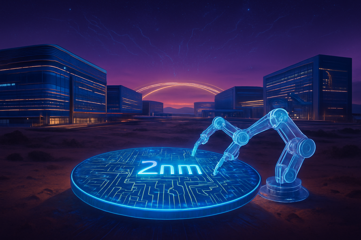
The Silicon Pact: Technical Specifications and the Roadmap to 2nm
The 2026 trade agreement introduces a sophisticated "reward for investment" mechanism. Specifically, Taiwanese companies expanding their U.S. capacity are granted exemptions from Section 232 duties, which previously added significant costs to steel, aluminum, and related derivative products used in fab construction. Under the new rules, companies like TSMC can import up to 2.5 times their planned U.S. capacity of wafers and chips duty-free during construction phases. Once operational, they retain a perpetual allowance to import 1.5 times their production capacity, creating a flexible hybrid supply chain that bridges the Pacific.
Technically, the Arizona Gigafab cluster is reaching unprecedented milestones. Fab 1 is currently in high-volume manufacturing (HVM) for 4nm and 5nm nodes, achieving yield rates of 88–92%—parity with TSMC’s flagship facilities in Hsinchu. Meanwhile, Fab 2 is entering the equipment installation phase for 3nm production, with a target start date in early 2027. Most ambitiously, foundation work for Fab 3 is now complete; this facility is designed to produce 2nm and A16 (1.6nm) chips featuring Gate-All-Around (GAA) transistor architecture. This roadmap ensures that by 2030, roughly 30% of TSMC’s global 2nm capacity will be located within the Arizona cluster.
This development differs from previous onshoring efforts by focusing on the entire ecosystem rather than just the fab itself. The trade deal specifically rewards the "clustering" of suppliers. Companies such as Chang Chun Group, Sunlit Chemical, and LCY Chemical have already opened facilities in Arizona to provide ultra-pure hydrogen peroxide and electronic-grade isopropyl alcohol. The arrival of ASML (NASDAQ: ASML) with a massive 56,000-square-foot training center in Phoenix further cements the region as a global hub for lithography expertise, marking a shift from a "satellite fab" model to a complete, vertically integrated industrial cluster.
Market Implications for AI Giants and Startups
The primary beneficiaries of the Arizona Gigafab cluster are the titans of the AI industry. Nvidia (NASDAQ: NVDA) has already designated the Arizona site as a primary production hub for its Blackwell-series GPUs, which are the backbone of modern large language models. Similarly, Apple (NASDAQ: AAPL) continues to utilize the cluster for its A-series and M-series chips, which now feature advanced Neural Engines for on-device generative AI. For these companies, the trade deal provides a "Made in USA" certification that is increasingly vital for government contracts and domestic security requirements.
Beyond the established giants, the cluster is attracting major investment from hyperscalers like Microsoft (NASDAQ: MSFT). Microsoft is reportedly sourcing its Maia 200 AI inference accelerators—built on the 3nm node—through the TSMC ecosystem and is prioritizing its Arizona-based data centers to reduce latency and logistical overhead. Even OpenAI, working through partnerships with Broadcom (NASDAQ: AVGO), is expected to leverage the Arizona cluster for its future custom-designed training and inference silicon. This shift represents a massive disruption to the traditional "hub-and-spoke" model, where silicon had to travel thousands of miles for packaging before returning to the U.S.
The strategic advantage for these companies lies in supply chain resilience. By capping duties and stabilizing the cost of materials, the Silicon Pact removes the volatility associated with geopolitical tensions in the Taiwan Strait. For startups and smaller AI labs, the emergence of a domestic cluster means more predictable lead times and potentially lower "cost-per-token" for AI inference as the domestic supply of high-end chips increases. The competition is now moving from who can design the best chip to who can secure the most capacity in the Arizona cluster.
Geopolitical Security and the Broader AI Landscape
The US-Taiwan trade deal is a cornerstone of a broader trend toward "techno-nationalism" and supply chain diversification. In the wider AI landscape, the Arizona cluster serves as a hedge against the single-point-of-failure risk that has loomed over the industry for a decade. By de-risking the manufacturing process, the U.S. and Taiwan are creating a "silicon shield" that is economic rather than purely military. This fits into the ongoing global trend of regionalizing high-tech manufacturing, similar to the EU’s efforts with its own Chips Act.
However, the rapid expansion of the Arizona cluster is not without concerns. The environmental impact on the arid Sonoran Desert is a frequent point of discussion. To address this, the 2026 agreement includes provisions for "green manufacturing" infrastructure, funding massive water recycling plants that allow fabs to reuse up to 98% of their industrial water. Furthermore, there are ongoing labor challenges, as the demand for highly specialized semiconductor engineers in Phoenix currently outstrips local supply, necessitating the ASML training centers and university partnerships funded by the trade deal.
Comparatively, this milestone is as significant as the original founding of TSMC in the 1980s. It represents the first time that the world’s most advanced lithography (3nm and below) has been successfully transplanted to a different continent at scale. The geopolitical significance of having NVIDIA Blackwell GPUs and future 2nm "superchips" manufactured in a domestic "Gigafab" cluster provides the U.S. with a level of technological sovereignty that seemed impossible only five years ago.
The Road Ahead: Packaging and 1.6nm Nodes
Looking toward the near-term, the next major development will be the integration of advanced packaging. Historically, even chips made in the U.S. had to be sent back to Taiwan for CoWoS (Chip-on-Wafer-on-Substrate) packaging. By late 2026, TSMC and Amkor Technology (NASDAQ: AMKR) are expected to finalize their domestic advanced packaging facilities in Arizona. This will create a "turnkey" solution where raw silicon enters the Phoenix site and emerges as a fully packaged, ready-to-deploy AI accelerator.
In the long term, the industry is watching the 1.6nm (A16) node. Experts predict that the Arizona cluster will be the first site outside of Taiwan to implement A16 technology, which is essential for the 1,000W+ superchips required for "General Purpose AI" (GPAI). The challenge will be maintaining the high yields as the technology moves toward the atomic limit. If TSMC can successfully transition its Arizona cluster to GAA transistors at 2nm and beyond, it will solidify the region as the premier semiconductor hub of the 21st century.
A New Era for American Silicon
The finalization of the US-Taiwan "Silicon Pact" in early 2026 marks the beginning of a new era for American manufacturing and global AI development. By reducing tariffs and incentivizing a dense cluster of suppliers, the trade deal has transformed Arizona into a global epicenter for advanced semiconductor fabrication. The key takeaways are clear: the AI hardware supply chain is no longer a fragile, trans-Pacific line, but a robust, domestic ecosystem capable of supporting the world's most demanding computational needs.
As we move through the remainder of 2026, the industry should watch for the first "Arizona-packaged" Blackwell GPUs and the progress of tool installation in Fab 2. This development's significance in AI history will likely be viewed as the moment the physical "foundations" of the AI revolution were finally secured. The long-term impact will be felt in every sector of the economy, from autonomous vehicles to personalized medicine, all powered by the silicon emerging from the Arizona desert.
This content is intended for informational purposes only and represents analysis of current AI developments.
TokenRing AI delivers enterprise-grade solutions for multi-agent AI workflow orchestration, AI-powered development tools, and seamless remote collaboration platforms.
For more information, visit https://www.tokenring.ai/.