Tag: Trillion-Parameter Models

  • NVIDIA Unleashes the ‘Vera Rubin’ Era: A Terascale Leap for Trillion-Parameter AI

    NVIDIA Unleashes the ‘Vera Rubin’ Era: A Terascale Leap for Trillion-Parameter AI

    As the calendar turns to early 2026, the artificial intelligence industry has reached a pivotal inflection point with the official production launch of NVIDIA’s (NASDAQ: NVDA) "Vera Rubin" architecture. First teased in mid-2024 and formally detailed at CES 2026, the Rubin platform represents more than just a generational hardware update; it is a fundamental shift in computing designed to transition the industry from large-scale language models to the era of agentic AI and trillion-parameter reasoning systems.

    The significance of this announcement cannot be overstated. By moving beyond the Blackwell generation, NVIDIA is attempting to solidify its "AI Factory" concept, delivering integrated, liquid-cooled rack-scale environments that function as a single, massive supercomputer. With the demand for generative AI showing no signs of slowing, the Vera Rubin platform arrives as the definitive infrastructure required to sustain the next decade of scaling laws, promising to slash inference costs while providing the raw horsepower needed for the first generation of autonomous AI agents.

    Technical Specifications: The Power of R200 and HBM4

    At the heart of the new architecture is the Rubin R200 GPU, a monolithic leap in silicon engineering featuring 336 billion transistors—a 1.6x density increase over its predecessor, Blackwell. For the first time, NVIDIA has introduced the Vera CPU, built on custom Armv9.2 "Olympus" cores. This CPU isn't just a support component; it features spatial multithreading and is being marketed as a standalone powerhouse capable of competing with traditional server processors from Intel (NASDAQ: INTC) and AMD (NASDAQ: AMD). Together, the Rubin GPU and Vera CPU form the "Rubin Superchip," a unified unit that eliminates data bottlenecks between the processor and the accelerator.

    Memory performance has historically been the primary constraint for trillion-parameter models, and Rubin addresses this via High Bandwidth Memory 4 (HBM4). Each R200 GPU is equipped with 288 GB of HBM4, delivering a staggering aggregate bandwidth of 22.2 TB/s. This is made possible through a deep partnership with memory giants like Samsung (KRX: 005930) and SK Hynix (KRX: 000660). To connect these components at scale, NVIDIA has debuted NVLink 6, which provides 3.6 TB/s of bidirectional bandwidth per GPU. In a standard NVL72 rack configuration, this enables an aggregate GPU-to-GPU bandwidth of 260 TB/s, a figure that reportedly exceeds the total bandwidth of the public internet.

    The industry’s initial reaction has been one of both awe and logistical concern. While the shift to NVFP4 (NVIDIA Floating Point 4) compute allows the R200 to deliver 50 Petaflops of performance for AI inference, the power requirements have ballooned. The Thermal Design Power (TDP) for a single Rubin GPU is now finalized at 2.3 kW. This high power density has effectively made liquid cooling mandatory for modern data centers, forcing a rapid infrastructure pivot for any enterprise or cloud provider hoping to deploy the new hardware.

    Competitive Implications: The AI Factory Moat

    The arrival of Vera Rubin further cements the dominance of major hyperscalers who can afford the massive capital expenditures required for these liquid-cooled "AI Factories." Companies like Microsoft (NASDAQ: MSFT), Alphabet (NASDAQ: GOOGL), and Amazon (NASDAQ: AMZN) have already moved to secure early capacity. Microsoft, in particular, is reportedly designing its "Fairwater" data centers specifically around the Rubin NVL72 architecture, aiming to scale to hundreds of thousands of Superchips in a single unified cluster. This level of scale provides a distinct strategic advantage, allowing these giants to train models that are orders of magnitude larger than what startups can currently afford.

    NVIDIA's strategic positioning extends beyond just the silicon. By booking over 50% of the world’s advanced "Chip-on-Wafer-on-Substrate" (CoWoS) packaging capacity for 2026, NVIDIA has created a supply chain moat that makes it difficult for competitors to match Rubin's volume. While AMD’s Instinct MI455X and Intel’s Falcon Shores remain viable alternatives, NVIDIA's full-stack approach—integrating the Vera CPU, the Rubin GPU, and the BlueField-4 DPU—presents a "sticky" ecosystem that is difficult for AI labs to leave. Specialized providers like CoreWeave, who recently secured a multi-billion dollar investment from NVIDIA, are also gaining an edge by guaranteeing early access to Rubin silicon ahead of general market availability.

    The disruption to existing products is already evident. As Rubin enters full production, the secondary market for older H100 and even early Blackwell chips is expected to see a price correction. For AI startups, the choice is becoming increasingly binary: either build on top of the hyperscalers' Rubin-powered clouds or face a significant disadvantage in training efficiency and inference latency. This "compute divide" is likely to accelerate a trend of consolidation within the AI sector throughout 2026.

    Broader Significance: Sustaining the Scaling Laws

    In the broader AI landscape, the Vera Rubin architecture is the physical manifestation of the industry's belief in the "scaling laws"—the theory that increasing compute and data will continue to yield more capable AI. By specifically optimizing for Mixture-of-Experts (MoE) models and agentic reasoning, NVIDIA is betting that the future of AI lies in "System 2" thinking, where models don't just predict the next word but pause to reason and execute multi-step tasks. This architecture provides the necessary memory and interconnect speeds to make such real-time reasoning feasible for the first time.

    However, the massive power requirements of Rubin have reignited concerns regarding the environmental impact of the AI boom. With racks pulling over 250 kW of power, the industry is under pressure to prove that the efficiency gains—such as Rubin's reported 10x reduction in inference token cost—outweigh the total increase in energy consumption. Comparison to previous milestones, like the transition from Volta to Ampere, suggests that while Rubin is exponentially more powerful, it also marks a transition into an era where power availability, rather than silicon design, may become the ultimate bottleneck for AI progress.

    There is also a geopolitical dimension to this launch. As "Sovereign AI" becomes a priority for nations like Japan, France, and Saudi Arabia, the Rubin platform is being marketed as the essential foundation for national AI sovereignty. The ability of a nation to host a "Rubin Class" supercomputer is increasingly seen as a modern metric of technological and economic power, much like nuclear energy or aerospace capabilities were in the 20th century.

    The Horizon: Rubin Ultra and the Road to Feynman

    Looking toward the near future, the Vera Rubin architecture is only the beginning of a relentless annual release cycle. NVIDIA has already outlined plans for "Rubin Ultra" in late 2027, which will feature 12 stacks of HBM4 and even larger packaging to support even more complex models. Beyond that, the company has teased the "Feynman" architecture for 2028, hinting at a roadmap that leads toward Artificial General Intelligence (AGI) support.

    Experts predict that the primary challenge for the Rubin era will not be hardware performance, but software orchestration. As models grow to encompass trillions of parameters across hundreds of thousands of chips, the complexity of managing these clusters becomes immense. We can expect NVIDIA to double down on its "NIM" (NVIDIA Inference Microservices) and CUDA-X libraries to simplify the deployment of agentic workflows. Use cases on the horizon include "digital twins" of entire cities, real-time global weather modeling with unprecedented precision, and the first truly reliable autonomous scientific discovery agents.

    One hurdle that remains is the high cost of entry. While the cost per token is dropping, the initial investment for a Rubin-based cluster is astronomical. This may lead to a shift in how AI services are billed, moving away from simple token counts to "value-based" pricing for complex tasks solved by AI agents. What happens next depends largely on whether the software side of the industry can keep pace with this sudden explosion in available hardware performance.

    A Landmark in AI History

    The release of the Vera Rubin platform is a landmark event that signals the maturity of the AI era. By integrating a custom CPU, revolutionary HBM4 memory, and a massive rack-scale interconnect, NVIDIA has moved from being a chipmaker to a provider of the world’s most advanced industrial infrastructure. The key takeaways are clear: the future of AI is liquid-cooled, massively parallel, and focused on reasoning rather than just generation.

    In the annals of AI history, the Vera Rubin architecture will likely be remembered as the bridge between "Chatbots" and "Agents." It provides the hardware foundation for the first trillion-parameter models capable of high-level reasoning and autonomous action. For investors and industry observers, the next few months will be critical to watch as the first "Fairwater" class clusters come online and we see the first real-world benchmarks from the R200 in the wild.

    The tech industry is no longer just competing on algorithms; it is competing on the physical reality of silicon, power, and cooling. In this new world, NVIDIA’s Vera Rubin is currently the unchallenged gold standard.


    This content is intended for informational purposes only and represents analysis of current AI developments.

    TokenRing AI delivers enterprise-grade solutions for multi-agent AI workflow orchestration, AI-powered development tools, and seamless remote collaboration platforms. For more information, visit https://www.tokenring.ai/.
  • The HBM4 Arms Race: SK Hynix, Samsung, and Micron Deliver 16-Hi Samples to NVIDIA to Power the 100-Trillion Parameter Era

    The HBM4 Arms Race: SK Hynix, Samsung, and Micron Deliver 16-Hi Samples to NVIDIA to Power the 100-Trillion Parameter Era

    The global race for artificial intelligence supremacy has officially moved beyond the GPU and into the very architecture of memory. As of January 22, 2026, the "Big Three" memory manufacturers—SK Hynix (KOSPI: 000660), Samsung Electronics (KOSPI: 005930), and Micron Technology (NASDAQ: MU)—have all confirmed the delivery of 16-layer (16-Hi) High Bandwidth Memory 4 (HBM4) samples to NVIDIA (NASDAQ: NVDA). This milestone marks a critical shift in the AI infrastructure landscape, transitioning from the incremental improvements of the HBM3e era to a fundamental architectural redesign required to support the next generation of "Rubin" architecture GPUs and the trillion-parameter models they are destined to run.

    The immediate significance of this development cannot be overstated. By moving to a 16-layer stack, memory providers are effectively doubling the data "bandwidth pipe" while drastically increasing the memory density available to a single processor. This transition is widely viewed as the primary solution to the "Memory Wall"—the performance bottleneck where the processing power of modern AI chips far outstrips the ability of memory to feed them data. With these 16-Hi samples now undergoing rigorous qualification by NVIDIA, the industry is bracing for a massive surge in AI training efficiency and the feasibility of 100-trillion parameter models, which were previously considered computationally "memory-bound."

    Breaking the 1024-Bit Barrier: The Technical Leap to HBM4

    HBM4 represents the most significant architectural overhaul in the history of high-bandwidth memory. Unlike previous generations that relied on a 1024-bit interface, HBM4 doubles the interface width to 2048-bit. This "wider pipe" allows for aggregate bandwidths exceeding 2.0 TB/s per stack. To meet NVIDIA’s revised "Rubin-class" specifications, these 16-Hi samples have been engineered to achieve per-pin data rates of 11 Gbps or higher. This technical feat is achieved by stacking 16 individual DRAM layers—each thinned to roughly 30 micrometers, or one-third the thickness of a human hair—within a JEDEC-mandated height of 775 micrometers.

    The most transformative technical change, however, is the integration of the "logic die." For the first time, the base die of the memory stack is being manufactured on high-performance foundry nodes rather than standard DRAM processes. SK Hynix has partnered with Taiwan Semiconductor Manufacturing Co. (NYSE: TSM) to produce these base dies using 12nm and 5nm nodes. This allows for "active memory" capabilities, where the memory stack itself can perform basic data pre-processing, reducing the round-trip latency to the GPU. Initial reactions from the AI research community suggest that this integration could improve energy efficiency by 30% and significantly reduce the heat generation that plagued early 12-layer HBM3e prototypes.

    The shift to 16-Hi stacks also enables unprecedented VRAM capacities. A single NVIDIA Rubin GPU equipped with eight 16-Hi HBM4 stacks can now boast between 384GB and 512GB of total VRAM. This capacity is essential for the inference of massive Large Language Models (LLMs) that previously required entire clusters of GPUs just to hold the model weights in memory. Industry experts have noted that the 16-layer transition was "the hardest in HBM history," requiring advanced packaging techniques like Mass Reflow Molded Underfill (MR-MUF) and, in Samsung’s case, the pioneering of copper-to-copper "hybrid bonding" to eliminate the need for micro-bumps between layers.

    The Tri-Polar Power Struggle: Market Positioning and Strategic Advantages

    The delivery of these samples has ignited a fierce competitive struggle for dominance in NVIDIA's lucrative supply chain. SK Hynix, currently the market leader, utilized CES 2026 to showcase a functional 48GB 16-Hi HBM4 package, positioning itself as the "frontrunner" through its "One Team" alliance with TSMC. By outsourcing the logic die to TSMC, SK Hynix has ensured its memory is perfectly "tuned" for the CoWoS (Chip-on-Wafer-on-Substrate) packaging that NVIDIA uses for its flagship accelerators, creating a formidable barrier to entry for its competitors.

    Samsung Electronics, meanwhile, is pursuing an "all-under-one-roof" turnkey strategy. By using its own 4nm foundry process for the logic die and its proprietary hybrid bonding technology, Samsung aims to offer NVIDIA a more streamlined supply chain and potentially lower costs. Despite falling behind in the HBM3e race, Samsung's aggressive acceleration to 16-Hi HBM4 is a clear bid to reclaim its crown. However, reports indicate that Samsung is also hedging its bets by collaborating with TSMC to ensure its 16-Hi stacks remain compatible with NVIDIA’s standard manufacturing flows.

    Micron Technology has carved out a unique position by focusing on extreme energy efficiency. At CES 2026, Micron confirmed that its HBM4 capacity for the entirety of 2026 is already "sold out" through advance contracts, despite its mass production slated for slightly later than SK Hynix. Micron’s strategy targets the high-volume inference market where power costs are the primary concern for hyperscalers. This three-way battle ensures that while NVIDIA remains the primary gatekeeper, the diversity of technical approaches—SK Hynix’s partnership model, Samsung’s vertical integration, and Micron’s efficiency focus—will prevent a single-supplier monopoly from forming.

    Beyond the Hardware: Implications for the Global AI Landscape

    The arrival of 16-Hi HBM4 marks a pivotal moment in the broader AI landscape, moving the industry toward "Scale-Up" architectures where a single node can handle massive workloads. This fits into the trend of "Trillion-Parameter Scaling," where the size of AI models is no longer limited by the physical space on a motherboard but by the density of the memory stacks. The ability to fit a 100-trillion parameter model into a single rack of Rubin-powered servers will drastically reduce the networking overhead that currently consumes up to 30% of training time in modern data centers.

    However, the wider significance of this development also brings concerns regarding the "Silicon Divide." The extreme cost and complexity of HBM4—which is reportedly five to seven times more expensive than standard DDR5 memory—threaten to widen the gap between tech giants like Microsoft (NASDAQ: MSFT) or Google (NASDAQ: GOOGL) and smaller AI startups. Furthermore, the reliance on advanced packaging and logic die integration makes the AI supply chain even more dependent on a handful of facilities in Taiwan and South Korea, raising geopolitical stakes. Much like the previous breakthroughs in Transformer architectures, the HBM4 milestone is as much about economic and strategic positioning as it is about raw gigabytes per second.

    The Road to HBM5 and Hybrid Bonding: What Lies Ahead

    Looking toward the near-term, the focus will shift from sampling to yield optimization. While SK Hynix and Samsung have delivered 16-Hi samples, the challenge of maintaining high yields across 16 layers of thinned silicon is immense. Experts predict that 2026 will be a year of "Yield Warfare," where the company that can most reliably produce these stacks at scale will capture the majority of NVIDIA's orders for the Rubin Ultra refresh expected in 2027.

    Beyond HBM4, the horizon is already showing signs of HBM5, which is rumored to explore 20-layer and 24-layer stacks. To achieve this without exceeding the physical height limits of GPU packages, the industry must fully transition to hybrid bonding—a process that fuses copper pads directly together without any intervening solder. This transition will likely turn memory makers into "semi-foundries," further blurring the line between storage and processing. We may soon see "Custom HBM," where AI labs like OpenAI or Anthropic design their own logic dies to be placed at the bottom of the memory stack, specifically optimized for their unique neural network architectures.

    Wrapping Up the HBM4 Revolution

    The delivery of 16-Hi HBM4 samples to NVIDIA by SK Hynix, Samsung, and Micron marks the end of memory as a simple commodity and the beginning of its era as a custom logic component. This development is arguably the most significant hardware milestone of early 2026, providing the necessary bandwidth and capacity to push AI models past the 100-trillion parameter threshold. As these samples move into the qualification phase, the success of each manufacturer will be defined not just by speed, but by their ability to master the complex integration of logic and memory.

    In the coming weeks and months, the industry should watch for NVIDIA’s official qualification results, which will determine the initial allocation of "slots" on the Rubin platform. The battle for HBM4 dominance is far from over, but the opening salvos have been fired, and the stakes—control over the fundamental building blocks of the AI era—could not be higher. For the technology industry, the HBM4 era represents the definitive breaking of the "Memory Wall," paving the way for AI capabilities that were, until now, strictly theoretical.


    This content is intended for informational purposes only and represents analysis of current AI developments.

    TokenRing AI delivers enterprise-grade solutions for multi-agent AI workflow orchestration, AI-powered development tools, and seamless remote collaboration platforms.
    For more information, visit https://www.tokenring.ai/.

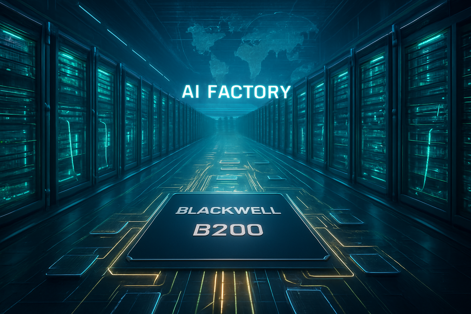
  • The Dawn of the AI Factory: NVIDIA Blackwell B200 Enters Full Production as Naver Scales Korea’s Largest AI Cluster

    The Dawn of the AI Factory: NVIDIA Blackwell B200 Enters Full Production as Naver Scales Korea’s Largest AI Cluster

    SANTA CLARA, CA — January 8, 2026 — The global landscape of artificial intelligence has reached a definitive turning point as NVIDIA (NASDAQ:NVDA) announced today that its Blackwell B200 architecture has entered full-scale volume production. This milestone marks the transition of the world’s most powerful AI chip from early-access trials to the backbone of global industrial intelligence. With supply chain bottlenecks for critical components like High Bandwidth Memory (HBM3e) and advanced packaging finally stabilizing, NVIDIA is now shipping Blackwell units in the tens of thousands per week, effectively sold out through mid-2026.

    The significance of this production ramp-up was underscored by South Korean tech titan Naver (KRX:035420), which recently completed the deployment of Korea’s largest AI computing cluster. Utilizing 4,000 Blackwell B200 GPUs, the "B200 4K Cluster" is designed to propel the next generation of "omni models"—systems capable of processing text, video, and audio simultaneously. Naver’s move signals a broader shift toward "AI Sovereignty," where nations and regional giants build massive, localized infrastructure to maintain a competitive edge in the era of trillion-parameter models.

    Redefining the Limits of Silicon: The Blackwell Architecture

    The Blackwell B200 is not merely an incremental upgrade; it represents a fundamental architectural shift from its predecessor, the H100 (Hopper). While the H100 was a monolithic chip, the B200 utilizes a revolutionary chiplet-based design, connecting two reticle-limited dies via a 10 TB/s ultra-high-speed link. This allows the 208 billion transistors to function as a single unified processor, effectively bypassing the physical limits of traditional silicon manufacturing. The B200 boasts 192GB of HBM3e memory and 8 TB/s of bandwidth, more than doubling the capacity and speed of previous generations.

    A key differentiator in the Blackwell era is the introduction of FP4 (4-bit floating point) precision. This technical leap, managed by a second-generation Transformer Engine, allows the B200 to process trillion-parameter models with 30 times the inference throughput of the H100. This capability is critical for the industry's pivot toward Mixture-of-Experts (MoE) models, where only a fraction of the model’s parameters are active at any given time, drastically reducing the energy cost per token. Initial reactions from the research community suggest that Blackwell has "reset the scaling laws," enabling real-time reasoning for models that were previously too large to serve efficiently.

    The "AI Factory" Era and the Corporate Arms Race

    NVIDIA CEO Jensen Huang has frequently described this transition as the birth of the "AI Factory." In this paradigm, data centers are no longer viewed as passive storage hubs but as industrial facilities where raw data is the raw material and "intelligence" is the finished product. This shift is visible in the strategic moves of hyperscalers and sovereign nations alike. While Naver is leading the charge in South Korea, global giants like Microsoft (NASDAQ:MSFT), Amazon (NASDAQ:AMZN), and Alphabet (NASDAQ:GOOGL) are integrating Blackwell into their clouds to support massive agentic systems—AI that doesn't just chat, but autonomously executes multi-step tasks.

    However, NVIDIA is not without challengers. As Blackwell hits full production, AMD (NASDAQ:AMD) has countered with its MI350 and MI400 series, the latter featuring up to 432GB of HBM4 memory. Meanwhile, Google has ramped up its TPU v7 "Ironwood" chips, and Amazon’s Trainium3 is gaining traction among startups looking for a lower "Nvidia Tax." These competitors are focusing on "Total Cost of Ownership" (TCO) and energy efficiency, aiming to capture the 30-40% of internal workloads that hyperscalers are increasingly moving toward custom silicon. Despite this, NVIDIA’s software moat—CUDA—and the sheer scale of the Blackwell rollout keep it firmly in the lead.

    Global Implications and the Sovereign AI Trend

    The deployment of the Blackwell architecture fits into a broader trend of "Sovereign AI," where countries recognize that AI capacity is as vital as energy or food security. Naver’s 4,000-GPU cluster is a prime example of this, providing South Korea with the computational self-reliance to develop foundation models like HyperCLOVA X without total dependence on Silicon Valley. Naver CEO Choi Soo-yeon noted that training tasks that previously took 18 months can now be completed in just six weeks, a 12-fold acceleration that fundamentally changes the pace of national innovation.

    Yet, this massive scaling brings significant concerns, primarily regarding energy consumption. A single GB200 NVL72 rack—a cluster of 72 Blackwell GPUs acting as one—can draw over 120kW of power, necessitating a mandatory shift toward liquid cooling solutions. The industry is now grappling with the "Energy Wall," leading to unprecedented investments in modular nuclear reactors and specialized power grids to sustain these AI factories. This has turned the AI race into a competition not just for chips, but for the very infrastructure required to keep them running.

    The Horizon: From Reasoning to Agency

    Looking ahead, the full production of Blackwell is expected to catalyze the move from "Reasoning AI" to "Agentic AI." Near-term developments will likely see the rise of autonomous systems capable of managing complex logistics, scientific discovery, and software development with minimal human oversight. Experts predict that the next 12 to 24 months will see the emergence of models exceeding 10 trillion parameters, powered by the Blackwell B200 and its already-announced successor, the Blackwell Ultra (B300), and the future "Rubin" (R100) architecture.

    The challenges remaining are largely operational and ethical. As AI factories begin producing "intelligence" at an industrial scale, the industry must address the environmental impact of such massive compute and the societal implications of increasingly autonomous agents. However, the momentum is undeniable. OpenAI CEO Sam Altman recently remarked that there is "no scaling wall" in sight, and the massive Blackwell deployment in early 2026 appears to validate that conviction.

    A New Chapter in Computing History

    In summary, the transition of the NVIDIA Blackwell B200 into full production is a landmark event that formalizes the "AI Factory" as the central infrastructure of the 21st century. With Naver’s massive cluster serving as a blueprint for national AI sovereignty and the B200’s technical specs pushing the boundaries of what is computationally possible, the industry has moved beyond the experimental phase of generative AI.

    As we move further into 2026, the focus will shift from the availability of chips to the efficiency of the factories they power. The coming months will be defined by how effectively companies and nations can translate this unprecedented raw compute into tangible economic and scientific breakthroughs. For now, the Blackwell era has officially begun, and the world is only starting to see the scale of the intelligence it will produce.


    This content is intended for informational purposes only and represents analysis of current AI developments.

    TokenRing AI delivers enterprise-grade solutions for multi-agent AI workflow orchestration, AI-powered development tools, and seamless remote collaboration platforms.
    For more information, visit https://www.tokenring.ai/.