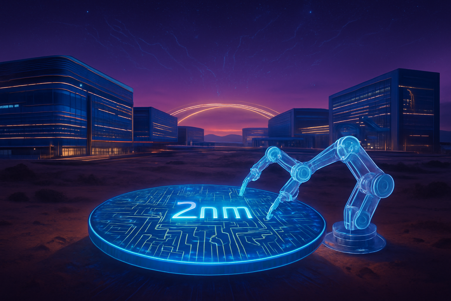
As of January 20, 2026, the global semiconductor landscape has officially entered a new epoch. Taiwan Semiconductor Manufacturing Company (NYSE: TSM) announced today that its 2-nanometer (N2) process technology has reached a critical mass production milestone, successfully ramping up high-volume manufacturing (HVM) at its lead facilities in Taiwan. This achievement marks the industry’s definitive transition into the "Angstrom Era," providing the essential hardware foundation for the next generation of generative AI models, autonomous systems, and ultra-efficient mobile computing.
The milestone is characterized by "better than expected" yield rates and an aggressive expansion of capacity across TSMC’s manufacturing hubs. By hitting these targets in early 2026, TSMC has solidified its position as the primary foundry for the world’s most advanced silicon, effectively setting the pace for the entire technology sector. The move to 2nm is not merely a shrink in size but a fundamental shift in transistor architecture that promises to redefine the limits of power efficiency and computational density.
The Nanosheet Revolution: Engineering the Future of Logic
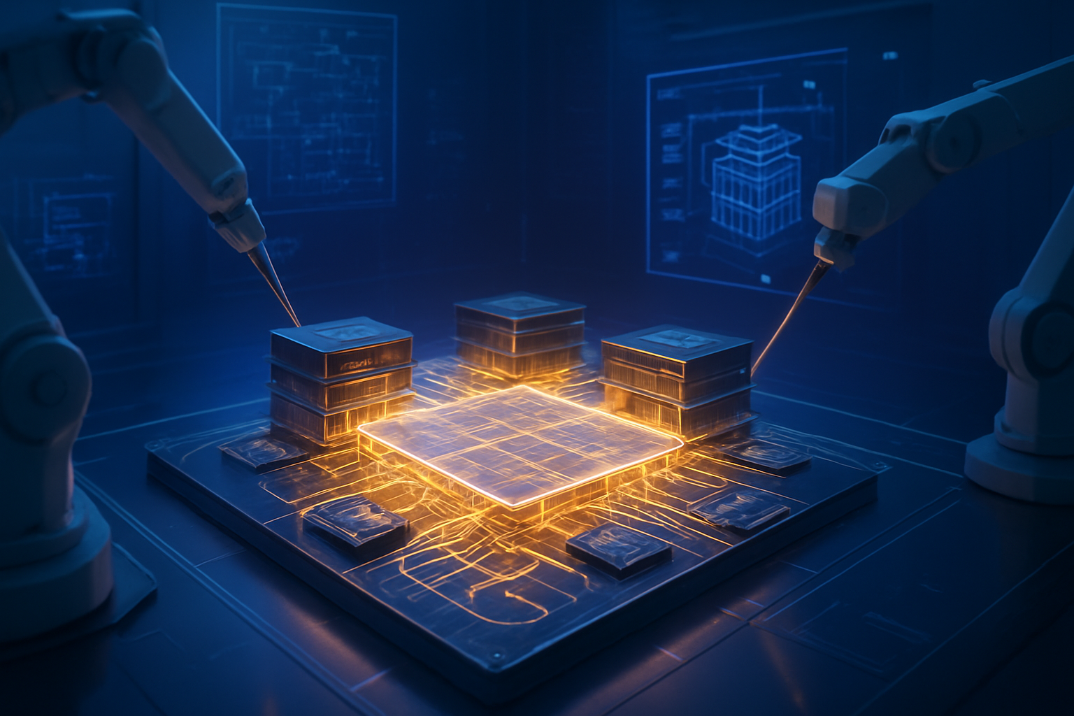
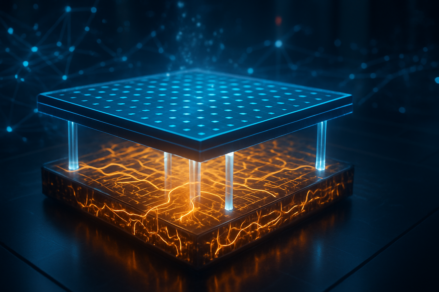
The 2nm node represents the most significant architectural departure for TSMC in over a decade: the transition from FinFET (Fin Field-Effect Transistor) to Nanosheet Gate-All-Around (GAAFET) transistors. In this new design, the gate surrounds the channel on all four sides, offering superior electrostatic control and virtually eliminating the electron leakage that had begun to plague FinFET designs at the 3nm barrier. Technical specifications released this month confirm that the N2 process delivers a 10–15% speed improvement at the same power level, or a staggering 25–30% power reduction at the same clock speed compared to the previous N3E node.
A standout feature of this milestone is the introduction of NanoFlex™ technology. This innovation allows chip designers—including engineers at Apple (NASDAQ: AAPL) and NVIDIA (NASDAQ: NVDA)—to mix and match different nanosheet widths within a single chip design. This granular control allows specific sections of a processor to be optimized for extreme performance while others are tuned for power sipping, a capability that industry experts say is crucial for the high-intensity, fluctuating workloads of modern AI inference. Initial reports from the Hsinchu (Baoshan) "gigafab" and the Kaohsiung site indicate that yield rates for 2nm logic test chips have stabilized between 70% and 80%, a remarkably high figure for the early stages of such a complex architectural shift.
Initial reactions from the semiconductor research community have been overwhelmingly positive. Dr. Aris Cheng, a senior analyst at the Global Semiconductor Alliance, noted, "TSMC's ability to maintain 70%+ yields while transitioning to GAAFET is a testament to their operational excellence. While competitors have struggled with the 'GAA learning curve,' TSMC appears to have bypassed the typical early-stage volatility." This reliability has allowed TSMC to secure massive volume commitments for 2026, ensuring that the next generation of flagship devices will be powered by 2nm silicon.
The Competitive Gauntlet: TSMC, Intel, and Samsung
The mass production milestone in January 2026 places TSMC in a fierce strategic position against its primary rivals. Intel (NASDAQ: INTC) has recently made waves with its 18A process, which technically beat TSMC to the market with backside power delivery—a feature Intel calls PowerVia. However, while Intel's Panther Lake chips have begun appearing in early 2026, analysts suggest that TSMC’s N2 node holds a significant lead in overall transistor density and manufacturing yield. TSMC is expected to introduce its own backside power delivery in the N2P node later this year, potentially neutralizing Intel's temporary advantage.
Meanwhile, Samsung Electronics (KRX: 005930) continues to face challenges in its 2nm (SF2) ramp-up. Although Samsung was the first to adopt GAA technology at the 3nm stage, it has struggled to lure high-volume customers away from TSMC due to inconsistent yield rates and thermal management issues. As of early 2026, TSMC remains the "indispensable" foundry, with its 2nm capacity already reportedly overbooked by long-term partners like Advanced Micro Devices (NASDAQ: AMD) and MediaTek.
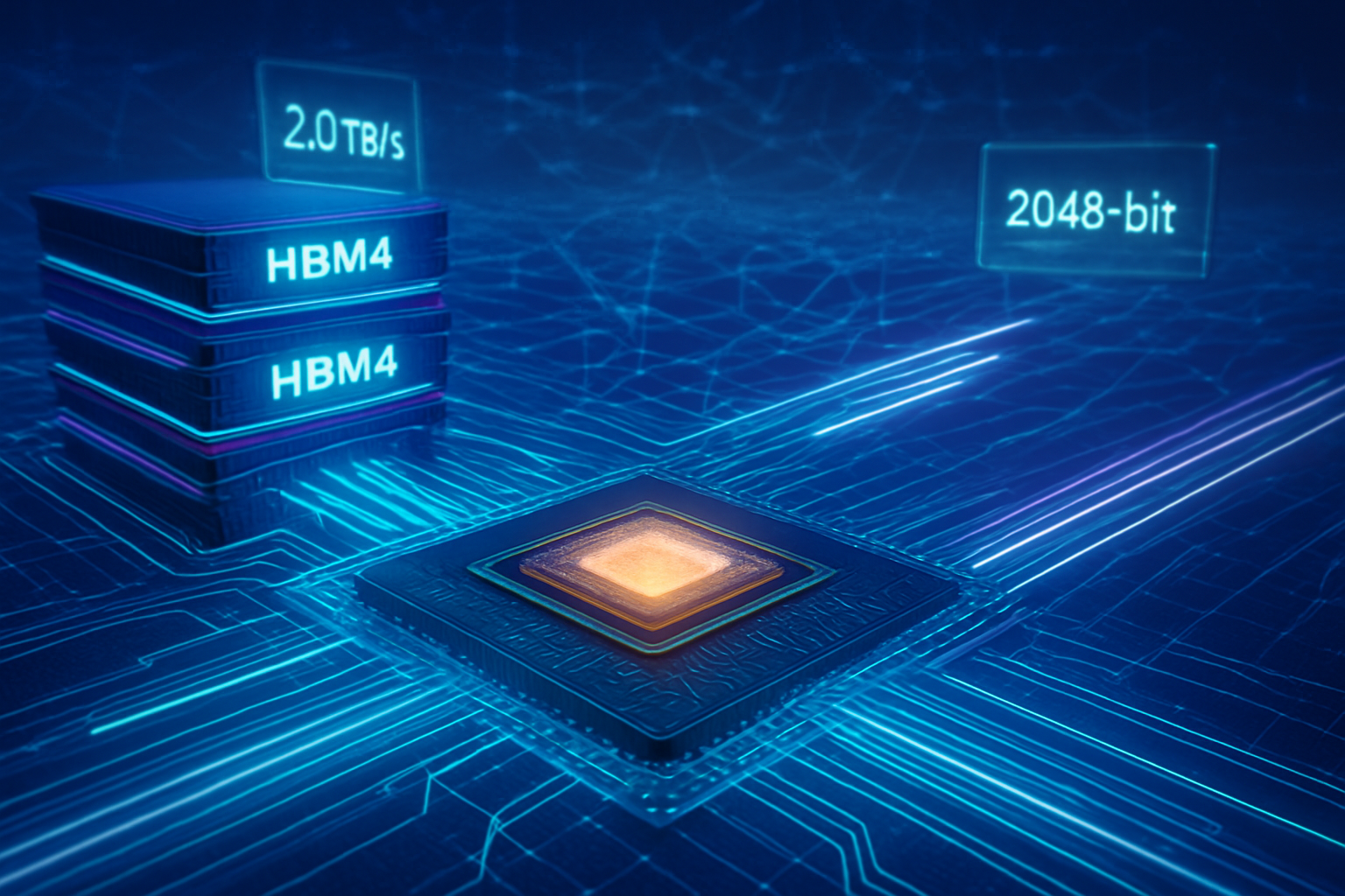
For AI giants, this milestone is a sigh of relief. The massive demand for Blackwell-successor GPUs from NVIDIA and custom AI accelerators from hyperscalers like Alphabet Inc. (NASDAQ: GOOGL) and Microsoft (NASDAQ: MSFT) relies entirely on TSMC’s ability to scale. The strategic advantage of 2nm lies in its ability to pack more AI "neurons" into the same thermal envelope, a critical requirement for the massive data centers powering the 2026 era of LLMs.
Global Footprints and the Arizona Timeline
While the production heart of the 2nm era remains in Taiwan, TSMC has provided updated clarity on its international expansion, particularly in the United States. Following intense pressure from U.S. clients and the Department of Commerce, TSMC has accelerated its timeline for Fab 21 in Arizona. Phase 1 is already in high-volume production of 4nm chips, but Phase 2, which will focus on 3nm production, is now slated for mass production in the second half of 2027.
More importantly, TSMC confirmed in January 2026 that Phase 3 of its Arizona site—the first U.S. facility planned for 2nm and the subsequent A16 (1.6nm) node—is on an "accelerated track." Groundbreaking occurred last year, and equipment installation is expected to begin in early 2027, with 2nm production on U.S. soil targeted for the 2028-2029 window. This geographic diversification is seen as a vital hedge against geopolitical instability in the Taiwan Strait, providing a "Silicon Shield" of sorts for the global AI economy.
The wider significance of this milestone cannot be overstated. It marks a moment where the physical limits of materials science are being pushed to their absolute edge to sustain the momentum of the AI revolution. Comparisons are already being made to the 2011 transition to FinFET; just as that shift enabled the smartphone decade, the move to 2nm Nanosheets is expected to enable the decade of the "Ambient AI"—where high-performance intelligence is embedded in every device without the constraint of massive power cords.
The Road to 14 Angstroms: What Lies Ahead
Looking past the immediate success of the 2nm milestone, TSMC’s roadmap is already extending into the late 2020s. The company has teased the A14 (1.4nm) node, which is currently in the R&D phase at the Hsinchu research center. Near-term developments will include the "N2P" and "N2X" variants, which will integrate backside power delivery and enhanced voltage rails for the most demanding high-performance computing applications.
However, challenges remain. The industry is reaching a point where traditional EUV (Extreme Ultraviolet) lithography may need to be augmented with High-NA (High Numerical Aperture) EUV machines—tools that cost upwards of $350 million each. TSMC has been cautious about adopting High-NA too early due to cost concerns, but the 2nm milestone suggests their current lithography strategy still has significant "runway." Experts predict that the next two years will be defined by a "density war," where the winner is decided not just by how small they can make a transistor, but by how many billions they can produce without defects.
A New Benchmark for the Silicon Age
The announcement of 2nm mass production in January 2026 is a watershed moment for the technology industry. It reaffirms TSMC’s role as the foundation of the modern digital world and provides the computational "fuel" needed for the next phase of artificial intelligence. By successfully navigating the transition to Nanosheet architecture and maintaining high yields in Hsinchu and Kaohsiung, TSMC has effectively set the technological standard for the next three to five years.
In the coming months, the focus will shift from manufacturing milestones to product reveals. Consumers can expect the first 2nm-powered smartphones and laptops to be announced by late 2026, promising battery lives and processing speeds that were previously considered theoretical. For now, the "Angstrom Era" has arrived, and it is paved with Taiwanese silicon.
This content is intended for informational purposes only and represents analysis of current AI developments.
TokenRing AI delivers enterprise-grade solutions for multi-agent AI workflow orchestration, AI-powered development tools, and seamless remote collaboration platforms.
For more information, visit https://www.tokenring.ai/.