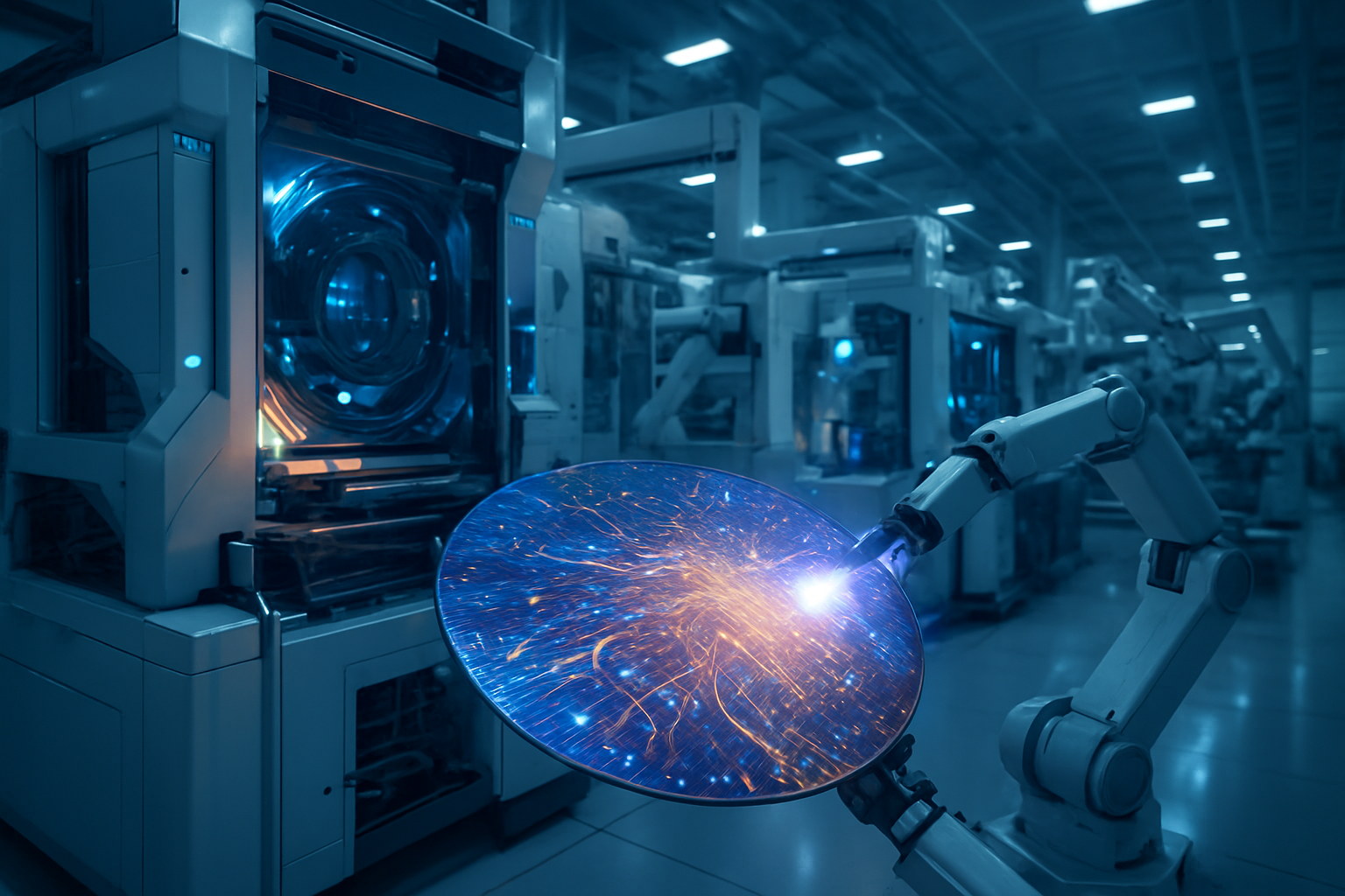
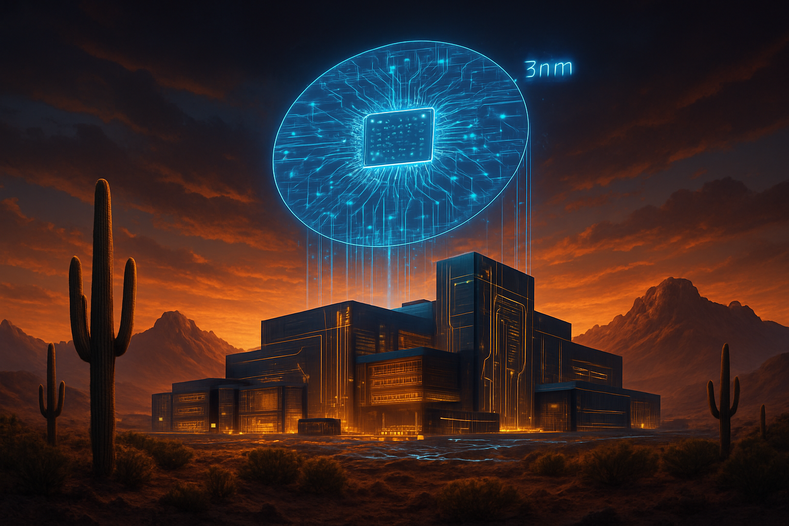
Tag: TSMC

  • Intel’s 1.8nm Era: Reclaiming the Silicon Crown as 18A Enters High-Volume Production

    Intel’s 1.8nm Era: Reclaiming the Silicon Crown as 18A Enters High-Volume Production

    SANTA CLARA, Calif. — In a historic milestone for the American semiconductor industry, Intel (NASDAQ: INTC) has officially announced that its 18A (1.8nm-class) process node has entered high-volume manufacturing (HVM). The announcement, made during the opening keynote of CES 2026, marks the successful completion of the company’s ambitious "five nodes in four years" roadmap. For the first time in nearly a decade, Intel appears to have parity—and by some technical measures, a clear lead—over its primary rival, Taiwan Semiconductor Manufacturing Company (NYSE: TSM), in the race to power the next generation of artificial intelligence.

    The immediate significance of 18A cannot be overstated. As AI models grow exponentially in complexity, the demand for chips that offer higher transistor density and significantly lower power consumption has reached a fever pitch. By reaching high-volume production with 18A, Intel is not just releasing a new processor; it is launching a fully-fledged foundry service capable of building the world’s most advanced AI accelerators for third-party clients. With anchor customers like Microsoft (NASDAQ: MSFT) and Amazon (NASDAQ: AMZN) already ramping up production on the node, the silicon landscape is undergoing its most radical shift since the invention of the integrated circuit.

    The Architecture of Leadership: RibbonFET and PowerVia

    The Intel 18A node represents a fundamental departure from the FinFET transistor architecture that has dominated the industry for over a decade. At the heart of 18A are two "world-first" technologies: RibbonFET and PowerVia. RibbonFET is Intel’s implementation of a Gate-All-Around (GAA) transistor, where the gate wraps entirely around the conducting channel. This provides superior electrostatic control, drastically reducing current leakage and allowing for higher drive currents at lower voltages. While TSMC (NYSE: TSM) has also moved to GAA with its N2 node, Intel’s 18A is distinguished by its integration of PowerVia—the industry’s first backside power delivery system.

    PowerVia solves one of the most persistent bottlenecks in chip design: "voltage droop" and signal interference. In traditional chips, power and signal lines are intertwined on the front side of the wafer, competing for space. PowerVia moves the entire power delivery network to the back of the wafer, leaving the front exclusively for data signals. This separation allows for a 15% to 25% improvement in performance-per-watt and enables chips to run at higher clock speeds without overheating. Initial data from early 18A production runs indicates that Intel has achieved a transistor density of approximately 238 million transistors per square millimeter (MTr/mm²), providing a potent combination of raw speed and energy efficiency that is specifically tuned for AI workloads.

    Industry experts have reacted with cautious optimism, noting that while TSMC’s N2 node still holds a slight lead in pure area density, Intel’s lead in backside power delivery gives it a strategic "performance-per-watt" advantage that is critical for massive data centers. "Intel has effectively leapfrogged the industry in power delivery architecture," noted one senior analyst at the event. "While the competition is still figuring out how to untangle their power lines, Intel is already shipping at scale."

    A New Titan in the Foundry Market

    The arrival of 18A transforms Intel Foundry from a theoretical competitor into a genuine threat to the TSMC-Samsung duopoly. By securing Microsoft (NASDAQ: MSFT) as a primary customer for its custom "Maia 2" AI accelerators, Intel has proven that its foundry model can attract the world’s largest "hyperscalers." Amazon (NASDAQ: AMZN) has similarly committed to 18A for its custom AI fabric and Graviton-series processors, seeking to reduce its reliance on external suppliers and optimize its internal cloud infrastructure for the generative AI era.

    This development creates a complex competitive dynamic for AI leaders like NVIDIA (NASDAQ: NVDA). While NVIDIA remains heavily reliant on TSMC for its current H-series and B-series GPUs, the company reportedly made a strategic $5 billion investment in Intel’s advanced packaging capabilities in 2025. With 18A now in high-volume production, the industry is watching closely to see if NVIDIA will shift a portion of its next-generation "Rubin" or "Post-Rubin" architecture to Intel’s fabs to diversify its supply chain and hedge against geopolitical risks in the Taiwan Strait.

    For startups and smaller AI labs, the emergence of a high-performance alternative in the United States could lower the barrier to entry for custom silicon. Intel’s "Secure Enclave" partnership with the U.S. Department of Defense further solidifies 18A as the premier node for sovereign AI applications, ensuring that the most sensitive government and defense chips are manufactured on American soil using the most advanced process technology available.

    The Geopolitics of Silicon and the AI Landscape

    The success of 18A is a pivotal moment for the broader AI landscape, which has been plagued by hardware shortages and energy constraints. As AI training clusters grow to consume hundreds of megawatts, the efficiency gains provided by PowerVia and RibbonFET are no longer just "nice-to-have" features—they are economic imperatives. Intel’s ability to deliver more "compute-per-watt" directly impacts the total cost of ownership for AI companies, potentially slowing the rise of energy costs associated with LLM (Large Language Model) development.

    Furthermore, 18A represents the first major fruit of the CHIPS and Science Act, which funneled billions into domestic semiconductor manufacturing. The fact that this node is being produced at scale in Fab 52 in Chandler, Arizona, signals a shift in the global center of gravity for high-end manufacturing. It alleviates concerns about the "single point of failure" in the global AI supply chain, providing a robust, domestic alternative to East Asian foundries.

    However, the transition is not without concerns. The complexity of 18A manufacturing is immense, and maintaining high yields at 1.8nm is a feat of engineering that requires constant vigilance. While current yields are reported in the 65%–75% range, any dip in production efficiency could lead to supply shortages or increased costs for customers. Comparisons to previous milestones, such as the transition to EUV (Extreme Ultraviolet) lithography, suggest that the first year of a new node is always a period of intense "learning by doing."

    The Road to 14A and High-NA EUV

    Looking ahead, Intel is already preparing the successor to 18A: the 14A (1.4nm) node. While 18A relies on standard 0.33 NA EUV lithography with multi-patterning, 14A will be the first node to fully utilize ASML (NASDAQ: ASML) High-NA (Numerical Aperture) EUV machines. Intel was the first in the industry to receive these "Twinscan EXE:5200" tools, and the company is currently using them for risk production and R&D to refine the 1.4nm process.

    The near-term roadmap includes the launch of Intel’s "Panther Lake" mobile processors and "Clearwater Forest" server chips, both built on 18A. These products will serve as the "canary in the coal mine" for the node’s real-world performance. If Clearwater Forest, with its massive 288-core count, can deliver on its promised efficiency gains, it will likely trigger a wave of data center upgrades across the globe. Experts predict that by 2027, the industry will transition into the "Angstrom Era" entirely, where 18A and 14A become the baseline for all high-end AI and edge computing devices.

    A Resurgent Intel in the AI History Books

    The entry of Intel 18A into high-volume production is more than just a technical achievement; it is a corporate resurrection. After years of delays and lost leadership, Intel has successfully executed a "Manhattan Project" style turnaround. By betting early on backside power delivery and securing the world’s first High-NA EUV tools, Intel has positioned itself as the primary architect of the hardware that will define the late 2020s.

    In the history of AI, the 18A node will likely be remembered as the point where hardware efficiency finally began to catch up with software ambition. The long-term impact will be felt in everything from the battery life of AI-integrated smartphones to the carbon footprint of massive neural network training runs. For the coming months, the industry will be watching yield reports and customer testimonials with intense scrutiny. If Intel can sustain this momentum, the "silicon crown" may stay in Santa Clara for a long time to come.


    This content is intended for informational purposes only and represents analysis of current AI developments.

    TokenRing AI delivers enterprise-grade solutions for multi-agent AI workflow orchestration, AI-powered development tools, and seamless remote collaboration platforms.
    For more information, visit https://www.tokenring.ai/.

  • The 2nm Revolution: TSMC Ignites Volume Production as Apple Secures the Future of Silicon

    The 2nm Revolution: TSMC Ignites Volume Production as Apple Secures the Future of Silicon

    The semiconductor landscape has officially shifted into a new era. As of January 9, 2026, Taiwan Semiconductor Manufacturing Company (NYSE:TSM) has successfully commenced the high-volume manufacturing of its 2-nanometer (N2) process node. This milestone marks the most significant architectural change in chip design in over a decade, as the industry moves away from the traditional FinFET structure to the cutting-edge Gate-All-Around (GAA) nanosheet technology.

    The immediate significance of this transition cannot be overstated. By shrinking transistors to the 2nm scale, TSMC is providing the foundational hardware necessary to power the next generation of artificial intelligence, high-performance computing (HPC), and mobile devices. With volume production now ramping up at Fab 20 in Hsinchu and Fab 22 in Kaohsiung, the first wave of 2nm-powered consumer electronics is expected to hit the market later this year, spearheaded by an exclusive capacity lock from the world’s most valuable technology company.

    Technical Foundations: The GAA Nanosheet Breakthrough

    The N2 node represents a departure from the "Fin" architecture that has dominated the industry since 2011. In the new GAA nanosheet design, the transistor gate surrounds the channel on all four sides. This provides superior electrostatic control, which drastically reduces current leakage—a persistent problem as transistors have become smaller and more densely packed. By wrapping the gate around the entire channel, TSMC can more precisely manage the flow of electrons, leading to a substantial leap in efficiency and performance.

    Technically, the N2 node offers a compelling value proposition over its predecessor, the 3nm (N3E) node. According to TSMC’s engineering data, the 2nm process delivers a 10% to 15% speed improvement at the same power consumption level, or a 25% to 30% reduction in power usage at the same clock speed. Furthermore, the node provides a 1.15x increase in chip density, allowing engineers to cram more logic and memory into the same physical footprint. This is particularly critical for AI accelerators, where transistor density directly correlates with the ability to process massive neural networks.

    Initial reactions from the semiconductor research community have been overwhelmingly positive, particularly regarding TSMC’s reported yield rates. While transitions to new architectures often suffer from low initial yields, reports indicate that TSMC has achieved nearly 70% yield during the early mass-production phase. This maturity distinguishes TSMC from its competitors, who have struggled to maintain stability while transitioning to GAA. Experts note that while the N2 node does not yet include backside power delivery—a feature reserved for the upcoming N2P variant—it introduces Super High-Performance Metal-Insulator-Metal (SHPMIM) capacitors, which double capacitance density to stabilize power delivery for high-load AI tasks.

    The Business of Silicon: Apple’s Strategic Dominance

    The launch of the N2 node has ignited a fierce strategic battle among tech giants, with Apple (NASDAQ:AAPL) emerging as the clear winner in the initial scramble for capacity. Apple has reportedly secured over 50% of TSMC’s total 2nm output through 2026. This massive "capacity lock" ensures that the upcoming iPhone 18 series, likely powered by the A20 Pro chip, will be the first consumer device to utilize 2nm silicon. By monopolizing the early supply, Apple creates a multi-year barrier for competitors, as rivals like Qualcomm (NASDAQ:QCOM) and MediaTek may have to wait until 2027 to access equivalent volumes of N2 wafers.

    This development places other industry leaders in a complex position. NVIDIA (NASDAQ:NVDA) and AMD (NASDAQ:AMD) are both high-priority customers for TSMC, but they are increasingly competing for the remaining 2nm capacity to fuel their next-generation AI GPUs and data center processors. The scarcity of 2nm wafers could lead to a tiered market where only the highest-margin products—such as NVIDIA’s Blackwell successors or AMD’s Instinct accelerators—can afford the premium pricing associated with the new node.

    For the broader market, TSMC’s success reinforces its position as the indispensable linchpin of the global tech economy. While Samsung (KRX:005930) was technically the first to introduce GAA with its 3nm node, it has faced persistent yield bottlenecks that have deterred major customers. Meanwhile, Intel (NASDAQ:INTC) is making a bold play with its 18A node, which features "PowerVia" backside power delivery. While Intel 18A may offer competitive raw performance, TSMC’s massive ecosystem and proven track record of high-volume reliability give it a strategic advantage that is currently unmatched in the foundry business.

    Global Implications: AI and the Energy Crisis

    The arrival of 2nm technology is a pivotal moment for the AI industry, which is currently grappling with the dual challenges of computing demand and energy consumption. As AI models grow in complexity, the power required to train and run them has skyrocketed, leading to concerns about the environmental impact of massive data centers. The 30% power efficiency gain offered by the N2 node provides a vital "pressure release valve," allowing AI companies to scale their operations without a linear increase in electricity usage.

    Furthermore, the 2nm milestone represents a continuation of Moore’s Law at a time when many predicted its demise. The shift to GAA nanosheets proves that through material science and architectural innovation, the industry can continue to shrink transistors and improve performance. However, this progress comes at a staggering cost. The price of a single 2nm wafer is estimated to be significantly higher than 3nm, potentially leading to a "silicon divide" where only the largest tech conglomerates can afford the most advanced hardware.

    Compared to previous milestones, such as the jump from 7nm to 5nm, the 2nm transition is more than just a shrink; it is a fundamental redesign of how electricity moves through a chip. This shift is essential for the "Edge AI" movement—bringing powerful, local AI processing to smartphones and wearable devices without draining their batteries in minutes. The success of the N2 node will likely determine which companies lead the next decade of ambient computing and autonomous systems.

    The Road Ahead: N2P and the 1.4nm Horizon

    Looking toward the near-term future, TSMC is already preparing for the next iteration of the 2nm platform. The N2P node, expected to enter production in late 2026, will introduce backside power delivery. This technology moves the power distribution network to the back of the silicon wafer, separating it from the signal wires on the front. This reduces interference and allows for even higher performance, setting the stage for the true peak of the 2nm era.

    Beyond 2026, the roadmap points toward the A14 (1.4nm) node. Research and development for A14 are already underway, with expectations that it will push the limits of extreme ultraviolet (EUV) lithography. The primary challenge moving forward will not just be the physics of the transistors, but the complexity of the packaging. TSMC’s CoWoS (Chip-on-Wafer-on-Substrate) and other 3D packaging technologies will become just as important as the node itself, as engineers look to stack 2nm chips to achieve unprecedented levels of performance.

    Experts predict that the next two years will see a "Foundry War" as Intel and Samsung attempt to reclaim market share from TSMC. Intel’s 18A is the most credible threat TSMC has faced in years, and the industry will be watching closely to see if Intel can deliver on its promise of "five nodes in four years." If Intel succeeds, it could break TSMC’s near-monopoly on advanced logic; if it fails, TSMC’s dominance will be absolute for the remainder of the decade.

    Conclusion: A New Standard for Excellence

    The commencement of 2nm volume production at TSMC is a defining moment for the technology industry in 2026. By successfully transitioning to GAA nanosheet transistors and securing the backing of industry titans like Apple, TSMC has once again set the gold standard for semiconductor manufacturing. The technical gains in power efficiency and performance will ripple through every sector of the economy, from the smartphones in our pockets to the massive AI clusters shaping the future of human knowledge.

    As we move through the first quarter of 2026, the key metrics to watch will be the continued ramp-up of wafer output and the performance benchmarks of the first 2nm chips. While challenges remain—including geopolitical tensions and the rising cost of fabrication—the successful launch of the N2 node ensures that the engine of digital innovation remains in high gear. The era of 2nm has arrived, and with it, the promise of a more efficient, powerful, and AI-driven future.


    This content is intended for informational purposes only and represents analysis of current AI developments.

    TokenRing AI delivers enterprise-grade solutions for multi-agent AI workflow orchestration, AI-powered development tools, and seamless remote collaboration platforms.
    For more information, visit https://www.tokenring.ai/.

  • The Backside Revolution: How PowerVia and A16 Are Rewiring the Future of AI Silicon

    The Backside Revolution: How PowerVia and A16 Are Rewiring the Future of AI Silicon

    As of January 8, 2026, the semiconductor industry has reached a historic inflection point that promises to redefine the limits of artificial intelligence hardware. For decades, chip designers have struggled with a fundamental physical bottleneck: the "front-side" delivery of power, where power lines and signal wires compete for the same cramped real estate on top of transistors. Today, that bottleneck is being shattered as Backside Power Delivery (BSPD) officially enters high-volume manufacturing, led by Intel Corporation (NASDAQ: INTC) and its groundbreaking 18A process.

    The shift to backside power—marketing-branded as "PowerVia" by Intel and "Super PowerRail" by Taiwan Semiconductor Manufacturing Company (NYSE: TSM)—is more than a mere manufacturing tweak; it is a fundamental architectural reorganization of the microchip. By moving the power delivery network to the underside of the silicon wafer, manufacturers are unlocking unprecedented levels of power efficiency and transistor density. This development arrives at a critical moment for the AI industry, where the ravenous energy demands of next-generation Large Language Models (LLMs) have threatened to outpace traditional hardware improvements.

    The Technical Leap: Decoupling Power from Logic

    Intel's 18A process, which reached high-volume manufacturing at Fab 52 in Chandler, Arizona, earlier this month, represents the first commercial deployment of Backside Power Delivery at scale. The core innovation, PowerVia, works by separating the intricate web of signal wires from the power delivery lines. In traditional chips, power must "tunnel" through up to 15 layers of metal interconnects to reach the transistors, leading to significant "voltage droop" and electrical interference. PowerVia eliminates this by routing power through the back of the wafer using Nano-Through Silicon Vias (nTSVs), providing a direct, low-resistance path to the transistors.

    The technical specifications of Intel 18A are formidable. By implementing PowerVia alongside RibbonFET (Gate-All-Around) transistors, Intel has achieved a 30% reduction in voltage droop and a 6% boost in clock frequency at identical power levels compared to previous generations. More importantly for AI chip designers, the technology allows for 90% standard cell utilization, drastically reducing the "wiring congestion" that often forces engineers to leave valuable silicon area empty. This leap in logic density—exceeding 30% over the Intel 3 node—means more AI processing cores can be packed into the same physical footprint.

    Initial reactions from the semiconductor research community have been overwhelmingly positive. Dr. Arati Prabhakar, Director of the White House Office of Science and Technology Policy, noted during a recent briefing that "the successful ramp of 18A is a validation of the 'five nodes in four years' strategy and a pivotal moment for domestic advanced manufacturing." Industry experts at SemiAnalysis have highlighted that Intel’s decision to decouple PowerVia from its first Gate-All-Around node (Intel 20A) allowed the company to de-risk the technology, giving them a roughly 18-month lead over TSMC in mastering the complexities of backside thinning and via alignment.

    The Competitive Landscape: Intel’s First-Mover Advantage vs. TSMC’s A16 Response

    The arrival of 18A has sent shockwaves through the foundry market, placing Intel Corporation (NASDAQ: INTC) in a rare position of technical leadership over TSMC. Intel has already secured major 18A commitments from Microsoft (NASDAQ: MSFT) and Amazon (NASDAQ: AMZN) for their custom AI accelerators, Maieutics and Trainium 3, respectively. By being the first to offer a mature BSPD solution, Intel Foundry is positioning itself as the premier destination for "AI-first" silicon, where thermal management and power delivery are the primary design constraints.

    However, TSMC is not standing still. The world’s largest foundry is preparing its response in the form of the A16 node, scheduled for high-volume manufacturing in the second half of 2026. TSMC’s implementation, known as Super PowerRail, is technically more ambitious than Intel’s PowerVia. While Intel uses nTSVs to connect to the metal layers, TSMC’s Super PowerRail connects the power network directly to the source and drain of the transistors. This "direct-contact" approach is significantly harder to manufacture but is expected to offer an 8-10% speed increase and a 15-20% power reduction, potentially leapfrogging Intel’s performance metrics by late 2026.

    The strategic battle lines are clearly drawn. Nvidia (NASDAQ: NVDA), the undisputed leader in AI hardware, has reportedly signed on as the anchor customer for TSMC’s A16 node to power its 2027 "Feynman" GPU architecture. Meanwhile, Apple (NASDAQ: AAPL) is rumored to be taking a more cautious approach, potentially skipping A16 for its mobile chips to focus on the N2P node, suggesting that backside power is currently viewed as a premium feature specifically optimized for high-performance computing and AI data centers rather than consumer mobile devices.

    Wider Significance: Solving the AI Power Crisis

    The transition to backside power delivery is a critical milestone in the broader AI landscape. As AI models grow in complexity, the "power wall"—the limit at which a chip can no longer be cooled or supplied with enough electricity—has become the primary obstacle to progress. BSPD effectively raises this wall. By reducing IR drop (voltage loss) and improving thermal dissipation, backside power allows AI accelerators to run at higher sustained workloads without throttling. This is essential for training the next generation of "Agentic AI" systems that require constant, high-intensity compute cycles.

    Furthermore, this development marks the end of the "FinFET era" and the beginning of the "Angstrom era." The move to 18A and A16 represents a transition where traditional scaling (making things smaller) is being replaced by architectural scaling (rearranging how things are built). This shift mirrors previous milestones like the introduction of High-K Metal Gate (HKMG) or EUV lithography, both of which were necessary to keep Moore’s Law alive. In 2026, the "Backside Revolution" is the new prerequisite for remaining competitive in the global AI arms race.

    There are, however, concerns regarding the complexity and cost of these new processes. Backside power requires extremely precise wafer thinning—grinding the silicon down to a fraction of its original thickness—and complex bonding techniques. These steps increase the risk of wafer breakage and lower initial yields. While Intel has reported healthy 18A yields in the 55-65% range, the high cost of these chips may further consolidate power in the hands of "Big Tech" giants like Alphabet (NASDAQ: GOOGL) and Meta (NASDAQ: META), who are the only ones capable of affording the multi-billion dollar design and fabrication costs associated with 1.6nm and 1.8nm silicon.

    The Road Ahead: 1.4nm and the Future of AI Accelerators

    Looking toward the late 2020s, the trajectory of backside power is clear: it will become the standard for all high-performance logic. Intel is already planning its "14A" node for 2027, which will refine PowerVia with even denser interconnects. Simultaneously, Samsung Electronics (OTC: SSNLF) is preparing its SF2Z node for 2027, which will integrate its own version of BSPDN into its third-generation Gate-All-Around (MBCFET) architecture. Samsung’s entry will likely trigger a price war in the advanced foundry space, potentially making backside power more accessible to mid-sized AI startups and specialized ASIC designers.

    Beyond 2026, we expect to see "Backside Power 2.0," where manufacturers begin to move other components to the back of the wafer, such as decoupling capacitors or even certain types of memory (like RRAM). This could lead to "3D-stacked" AI chips where the logic is sandwiched between a backside power delivery layer and a front-side memory cache, creating a truly three-dimensional computing environment. The primary challenge remains the thermal density; as chips become more efficient at delivering power, they also become more concentrated heat sources, necessitating new liquid cooling or "on-chip" cooling technologies.

    Conclusion: A New Foundation for Artificial Intelligence

    The arrival of Intel’s 18A and the looming shadow of TSMC’s A16 mark the beginning of a new chapter in semiconductor history. Backside Power Delivery has transitioned from a laboratory curiosity to a commercial reality, providing the electrical foundation upon which the next decade of AI innovation will be built. By solving the "routing congestion" and "voltage droop" issues that have plagued chip design for years, PowerVia and Super PowerRail are enabling a new class of processors that are faster, cooler, and more efficient.

    The significance of this development cannot be overstated. In the history of AI, we will look back at 2026 as the year the industry "flipped the chip" to keep the promise of exponential growth alive. For investors and tech enthusiasts, the coming months will be defined by the ramp-up of Intel’s Panther Lake and Clearwater Forest processors, providing the first real-world benchmarks of what backside power can do. As TSMC prepares its A16 risk production in the first half of 2026, the battle for silicon supremacy has never been more intense—or more vital to the future of technology.


    This content is intended for informational purposes only and represents analysis of current AI developments.

    TokenRing AI delivers enterprise-grade solutions for multi-agent AI workflow orchestration, AI-powered development tools, and seamless remote collaboration platforms.
    For more information, visit https://www.tokenring.ai/.

  • TSMC Enters the 2nm Era: A New Dawn for AI Supremacy as Volume Production Begins

    TSMC Enters the 2nm Era: A New Dawn for AI Supremacy as Volume Production Begins

    As the calendar turns to early 2026, the global semiconductor landscape has reached a pivotal inflection point. Taiwan Semiconductor Manufacturing Company (TSM:NYSE), the world’s largest contract chipmaker, has officially commenced volume production of its highly anticipated 2-nanometer (N2) process node. This milestone, centered at the company’s massive Fab 20 in Hsinchu and the newly repurposed Fab 22 in Kaohsiung, marks the first time the industry has transitioned away from the long-standing FinFET transistor architecture to the revolutionary Gate-All-Around (GAA) nanosheet technology.

    The immediate significance of this development cannot be overstated. With initial yield rates reportedly exceeding 65%—a remarkably high figure for a first-generation architectural shift—TSMC is positioning itself to capture an unprecedented 95% of the AI accelerator market. As AI demand continues to surge across every sector of the global economy, the 2nm node is no longer just a technical upgrade; it is the essential bedrock for the next generation of large language models, autonomous systems, and "Physical AI" applications.

    The Nanosheet Revolution: Inside the N2 Architecture

    The transition to the N2 node represents the most significant architectural change in chip manufacturing in over a decade. By moving from FinFET to GAAFET (Gate-All-Around Field-Effect Transistor) nanosheet technology, TSMC has effectively re-engineered how electrons flow through a chip. In this new design, the gate surrounds the channel on all four sides, providing superior electrostatic control, drastically reducing current leakage, and allowing for much finer tuning of performance and power consumption.

    Technically, the N2 node delivers a substantial leap over the previous 3nm (N3E) generation. According to official specifications, the new process offers a 10% to 15% increase in processing speed at the same power level, or a staggering 25% to 30% reduction in power consumption at the same speed. Furthermore, logic density has seen a boost of approximately 15%, allowing designers to pack more transistors into the same footprint. This is complemented by TSMC’s "Nano-Flex" technology, which allows chip designers to mix different nanosheet heights within a single block to optimize for either extreme performance or ultra-low power.

    Initial reactions from the AI research community and industry experts have been overwhelmingly positive. Analysts at JPMorgan (JPM:NYSE) and Goldman Sachs (GS:NYSE) have characterized the N2 launch as the start of a "multi-year AI supercycle." The industry is particularly impressed by the maturity of the ecosystem; unlike previous node transitions that faced years of delay, TSMC’s 2nm ramp-up has met every internal milestone, providing a stable foundation for the world's most complex silicon designs.

    A 1.5x Surge in Tape-Outs: The Strategic Advantage for Tech Giants

    The business impact of the 2nm node is already visible in the sheer volume of customer engagement. Reports indicate that the N2 family has recorded 1.5 times more "tape-outs"—the final stage of the design process before manufacturing—than the 3nm node did at the same point in its lifecycle. This surge is driven by a unique convergence: for the first time, mobile giants like Apple (AAPL:NASDAQ) and high-performance computing (HPC) leaders like NVIDIA (NVDA:NASDAQ) and Advanced Micro Devices (AMD:NASDAQ) are racing for the same leading-edge capacity simultaneously.

    AMD has notably used the 2nm transition to execute a strategic "leapfrog" over its competitors. At CES 2026, Dr. Lisa Su confirmed that the new Instinct MI400 series AI accelerators are built on TSMC’s N2 process, whereas NVIDIA's recently unveiled "Vera Rubin" architecture utilizes an enhanced 3nm (N3P) node. This gives AMD a temporary edge in raw transistor density and energy efficiency, particularly for memory-intensive LLM training. Meanwhile, Apple has secured over 50% of the initial 2nm capacity for its upcoming A20 chips, ensuring that the next generation of iPhones will maintain a significant lead in on-device AI processing.

    The competitive implications for other foundries are stark. While Intel (INTC:NASDAQ) is pushing its 18A node and Samsung (SSNLF:OTC) is refining its own GAA process, TSMC’s 95% projected market share in AI accelerators suggests a widening "foundry gap." TSMC’s moat is not just the silicon itself, but its advanced packaging ecosystem, specifically CoWoS (Chip on Wafer on Substrate), which is essential for the multi-die configurations used in modern AI GPUs.

    Silicon Sovereignty and the Broader AI Landscape

    The successful ramp of 2nm production at Fab 20 and Fab 22 carries immense weight in the broader context of "Silicon Sovereignty." As nations race to secure their AI supply chains, TSMC’s ability to deliver 2nm at scale reinforces Taiwan's position as the indispensable hub of the global tech economy. This development fits into a larger trend where the bottleneck for AI progress has shifted from software algorithms to the physical availability of advanced silicon and the energy required to run it.

    The power efficiency gains of the N2 node—up to 30%—are perhaps its most critical contribution to the AI landscape. With data centers consuming an ever-growing share of the world’s electricity, the ability to perform more "tokens per watt" is the only sustainable path forward for the AI industry. Comparisons are already being made to the 7nm breakthrough of 2018, which enabled the first wave of modern mobile computing; however, the 2nm era is expected to have a far more profound impact on infrastructure, enabling the transition from cloud-based AI to ubiquitous, "always-on" intelligence in edge devices and robotics.

    However, this concentration of power also raises concerns. The projected 95% market share for AI accelerators creates a single point of failure for the global AI economy. Any disruption to TSMC’s 2nm production lines could stall the progress of thousands of AI startups and tech giants alike. This has led to intensified efforts by hyperscalers like Amazon (AMZN:NASDAQ), Google (GOOGL:NASDAQ), and Microsoft (MSFT:NASDAQ) to design their own custom AI ASICs on N2, attempting to gain some measure of control over their hardware destinies.

    The Road to 1.4nm and Beyond: What’s Next for TSMC?

    Looking ahead, the 2nm node is merely the first chapter in a new book of semiconductor physics. TSMC has already outlined its roadmap for the second half of 2026, which includes the N2P (performance-enhanced) node and the introduction of the A16 (1.6-nanometer) process. The A16 node will be the first to feature Backside Power Delivery (BSPD), a technique that moves the power wiring to the back of the wafer to further improve efficiency and signal integrity.

    Experts predict that the primary challenge moving forward will be the integration of these advanced chips with next-generation memory, such as HBM4. As chip density increases, the "memory wall"—the gap between processor speed and memory bandwidth—becomes the new limiting factor. We can expect to see TSMC deepen its partnerships with memory leaders like SK Hynix and Micron (MU:NASDAQ) to create integrated 3D-stacked solutions that blur the line between logic and memory.

    In the long term, the focus will shift toward the A14 node (1.4nm), currently slated for 2027-2028. The industry is watching closely to see if the nanosheet architecture can be scaled that far, or if entirely new materials, such as carbon nanotubes or two-dimensional semiconductors, will be required. For now, the successful execution of N2 provides a clear runway for the next three years of AI innovation.

    Conclusion: A Landmark Moment in Computing History

    The commencement of 2nm volume production in early 2026 is a landmark achievement that cements TSMC’s dominance in the semiconductor industry. By successfully navigating the transition to GAA nanosheet technology and securing a massive 1.5x surge in tape-outs, the company has effectively decoupled itself from the traditional cycles of the chip market, becoming an essential utility for the AI era.

    The key takeaway for the coming months is the rapid shift in the competitive landscape. With AMD and Apple leading the charge onto 2nm, the pressure is now on NVIDIA and Intel to prove that their architectural innovations can compensate for a lag in process technology. Investors and industry watchers should keep a close eye on the output levels of Fab 20 and Fab 22; their success will determine the pace of AI advancement for the remainder of the decade. As we look toward the mid-2020s, it is clear that the 2nm era is not just about smaller transistors—it is about the limitless potential of the silicon that powers our world.


    This content is intended for informational purposes only and represents analysis of current AI developments.

    TokenRing AI delivers enterprise-grade solutions for multi-agent AI workflow orchestration, AI-powered development tools, and seamless remote collaboration platforms.
    For more information, visit https://www.tokenring.ai/.

  • The Great Silicon Homecoming: How Reshoring Redrew the Global AI Map in 2026

    The Great Silicon Homecoming: How Reshoring Redrew the Global AI Map in 2026

    As of January 8, 2026, the global semiconductor landscape has undergone its most radical transformation since the invention of the integrated circuit. The ambitious "reshoring" initiatives launched in the wake of the 2022 supply chain crises have reached a critical tipping point. For the first time in decades, the world’s most advanced artificial intelligence processors are rolling off production lines in the Arizona desert, while Japan’s "Rapidus" moonshot has defied skeptics by successfully piloting 2nm logic. This shift marks the end of the "Taiwan-only" era for high-end silicon, replaced by a fragmented but more resilient "Silicon Shield" spanning the U.S., Japan, and a pivoting European Union.

    The immediate significance of this development cannot be overstated. In a landmark achievement this month, Intel Corp. (NASDAQ: INTC) officially commenced high-volume manufacturing of its 18A (1.8nm-class) process at its Ocotillo campus in Arizona. This milestone, coupled with the successful ramp-up of NVIDIA Corp. (NASDAQ: NVDA) Blackwell GPUs at Taiwan Semiconductor Manufacturing Co. (NYSE: TSM) Arizona Fab 21, means that the hardware powering the next generation of generative AI is no longer a single-point-of-failure risk. However, this progress has come at a steep price: a new era of "equity-for-chips" has seen the U.S. government take a 10% federal stake in Intel to stabilize the domestic champion, signaling a permanent marriage between state interests and silicon production.

    The Technical Frontier: 18A, 2nm, and the Packaging Gap

    The technical achievements of early 2026 are defined by the industry's successful leap over the "2nm wall." Intel’s 18A process is the first in the world to implement High-NA EUV (Extreme Ultraviolet) lithography at scale, allowing for transistor densities that were theoretical just three years ago. By utilizing "PowerVia" backside power delivery and RibbonFET gate-all-around (GAA) architectures, these domestic chips offer a 15% performance-per-watt improvement over the 3nm nodes currently dominating the market. This advancement is critical for AI data centers, which are increasingly constrained by power consumption and thermal limits.

    While the U.S. has focused on "brute force" logic manufacturing, Japan has taken a more specialized technical path. Rapidus, the state-backed Japanese venture, surprised the industry in July 2025 by demonstrating operational 2nm GAA transistors at its Hokkaido pilot line. Unlike the massive, multi-product "mega-fabs" of the past, Japan’s strategy involves "Short TAT" (Turnaround Time) manufacturing, designed specifically for the rapid prototyping of custom AI accelerators. This allows AI startups to move from design to silicon in half the time required by traditional foundries, creating a technical niche that neither the U.S. nor Taiwan currently occupies.

    Despite these logic breakthroughs, a significant technical "chokepoint" remains: Advanced Packaging. Even as "Made in USA" wafers emerge from Arizona, many must still be shipped back to Asia for Chip-on-Wafer-on-Substrate (CoWoS) assembly—the process required to link HBM3e memory to GPU logic. While Amkor Technology, Inc. (NASDAQ: AMKR) has begun construction on domestic advanced packaging facilities, they are not expected to reach high-volume scale until 2027. This "packaging gap" remains the final technical hurdle to true semiconductor sovereignty.

    Competitive Realignment: Giants and Stakeholders

    The reshoring movement has created a new hierarchy among tech giants. NVIDIA and Advanced Micro Devices, Inc. (NASDAQ: AMD) have emerged as the primary beneficiaries of the "multi-fab" strategy. By late 2025, NVIDIA successfully diversified its supply chain, with its Blackwell architecture now split between Taiwan and Arizona. This has not only mitigated geopolitical risk but also allowed NVIDIA to negotiate more favorable pricing as TSMC faces domestic competition from a revitalized Intel Foundry. AMD has followed suit, confirming at CES 2026 that its 5th Generation EPYC "Venice" CPUs are now being produced domestically, providing a "sovereign silicon" option for U.S. government and defense contracts.

    For Intel, the reshoring journey has been a double-edged sword. While it has secured its position as the "National Champion" of U.S. silicon, its financial struggles in 2024 led to a historic restructuring. Under the "U.S. Investment Accelerator" program, the Department of Commerce converted billions in CHIPS Act grants into a 10% non-voting federal equity stake. This move has stabilized Intel’s balance sheet but has also introduced unprecedented government oversight into its strategic roadmap. Meanwhile, Samsung Electronics (KRX: 005930) has faced challenges in its Taylor, Texas facility, delaying mass production to late 2026 as it pivots its target node from 4nm to 2nm to attract high-performance computing (HPC) customers who have already committed to TSMC’s Arizona capacity.

    The European landscape presents a stark contrast. The cancellation of Intel’s Magdeburg "Mega-fab" in late 2025 served as a wake-up call for the EU. In response, the European Commission has pivoted toward the "EU Chips Act 2.0," focusing on "Value over Volume." Rather than trying to compete in leading-edge logic, Europe is doubling down on power semiconductors and automotive chips through STMicroelectronics (NYSE: STM) and GlobalFoundries Inc. (NASDAQ: GFS), ensuring that while they may not lead in AI training chips, they remain the dominant force in the silicon that powers the green energy transition and autonomous vehicles.

    Geopolitical Significance and the "Sovereign AI" Trend

    The reshoring of chip manufacturing is the physical manifestation of the "Sovereign AI" movement. In 2026, nations no longer view AI as a software challenge, but as a resource-extraction challenge where the "resource" is compute. The CHIPS Act in the U.S., the EU Chips Act, and Japan’s massive subsidies have successfully broken the "Taiwan-centric" model of the 2010s. This has led to a more stable global supply chain, but it has also led to "silicon nationalism," where the most advanced chips are subject to increasingly complex export controls and domestic-first allocation policies.

    Comparisons to previous milestones, such as the 1970s oil crisis, are frequent among industry analysts. Just as nations sought energy independence then, they seek "compute independence" now. The successful reshoring of 4nm and 1.8nm nodes to the U.S. and Japan acts as a "Silicon Shield," theoretically deterring conflict by reducing the catastrophic global impact of a potential disruption in the Taiwan Strait. However, critics point out that this has also led to a significant increase in the cost of AI hardware. Domestic manufacturing in the U.S. and Europe remains 20-30% more expensive than in Taiwan, a "reshoring tax" that is being passed down to enterprise AI customers.

    Furthermore, the environmental impact of these "Mega-fabs" has become a central point of contention. The massive water and energy requirements of the new Arizona and Ohio facilities have sparked local debates, forcing companies to invest billions in water reclamation technology. As the AI landscape shifts from "training" to "inference," the demand for these chips will only grow, making the sustainability of reshored manufacturing a key geopolitical metric in the years to come.

    The Horizon: 2027 and Beyond

    Looking toward the late 2020s, the industry is preparing for the "Angstrom Era." Intel, TSMC, and Samsung are all racing toward 14A (1.4nm) processes, with plans to begin equipment move-in for these nodes by 2027. The next frontier for reshoring will not be the chip itself, but the materials science behind it. We expect to see a surge in domestic investment for the production of high-purity chemicals and specialized wafers, reducing the reliance on a few key suppliers in China and Japan.

    The most anticipated development is the integration of "Silicon Photonics" and 3D stacking, which will likely be the first technologies to be "born reshored." Because these technologies are still in their infancy, the U.S. and Japan are building the manufacturing infrastructure alongside the R&D, avoiding the need to "pull back" production from overseas. Experts predict that by 2028, the "Packaging Gap" will be fully closed, with Arizona and Hokkaido housing the world’s most advanced automated assembly lines, capable of producing a finished AI supercomputer module entirely within a single geographic region.

    A New Chapter in Industrial Policy

    The reshoring of chip manufacturing will be remembered as the most significant industrial policy experiment of the 21st century. As of early 2026, the results are a qualified success: the U.S. has reclaimed its status as a leading-edge manufacturer, Japan has staged a stunning comeback, and the global AI supply chain is more diversified than at any point in history. The "Silicon Shield" has been successfully extended, providing a much-needed buffer for the booming AI economy.

    However, the journey is far from over. The cancellation of major projects in Europe and the delays in the U.S. "Silicon Heartland" of Ohio serve as reminders that building the world’s most complex machines is a decade-long endeavor, not a four-year political cycle. In the coming months, the industry will be watching the first yields of Samsung’s 2nm Texas fab and the progress of the EU’s new "Value over Volume" strategy. For now, the "Great Silicon Homecoming" has proven that with enough capital and political will, the map of the digital world can indeed be redrawn.


    This content is intended for informational purposes only and represents analysis of current AI developments.

    TokenRing AI delivers enterprise-grade solutions for multi-agent AI workflow orchestration, AI-powered development tools, and seamless remote collaboration platforms.
    For more information, visit https://www.tokenring.ai/.

  • The Silicon Renaissance: How AI is Propelling the Semiconductor Industry Toward the $1 Trillion Milestone

    The Silicon Renaissance: How AI is Propelling the Semiconductor Industry Toward the $1 Trillion Milestone

    As of early 2026, the global semiconductor industry has officially entered what analysts are calling the "Silicon Super-Cycle." Long characterized by its volatile boom-and-bust cycles, the sector has undergone a structural transformation, evolving from a provider of cyclical components into the foundational infrastructure of a new sovereign economy. Following a record-breaking 2025 that saw global revenues surge past $800 billion, consensus from major firms like McKinsey, Gartner, and IDC now confirms that the industry is on a definitive, accelerated path to exceed $1 trillion in annual revenue by 2030—with some aggressive forecasts suggesting the milestone could be reached as early as 2028.

    The primary catalyst for this historic expansion is the insatiable demand for artificial intelligence, specifically the transition from simple generative chatbots to "Agentic AI" and "Physical AI." This shift has fundamentally rewired the global economy, turning compute capacity into a metric of national productivity. As the digital economy expands into every facet of industrial manufacturing, automotive transport, and healthcare, the semiconductor has become the "new oil," driving a massive wave of capital expenditure that is reshaping the geopolitical and corporate landscape of the 21st century.

    The Angstrom Era: 2nm Nodes and the HBM4 Revolution

    Technically, the road to $1 trillion is being paved with the most complex engineering feats in human history. As of January 2026, the industry has successfully transitioned into the "Angstrom Era," marked by the high-volume manufacturing of sub-2nm class chips. Taiwan Semiconductor Manufacturing Company (NYSE: TSM) began mass production of its 2nm (N2) node in late 2025, utilizing Nanosheet Gate-All-Around (GAA) transistors for the first time. This architecture replaces the decade-old FinFET design, allowing for a 30% reduction in power consumption—a critical requirement for the massive data centers powering today's trillion-parameter AI models. Meanwhile, Intel Corporation (NASDAQ: INTC) has made a significant comeback, reaching high-volume manufacturing on its 18A (1.8nm) node this week. Intel’s 18A is the first in the industry to combine GAA transistors with "PowerVia" backside power delivery, a technical leap that many experts believe could finally level the playing field with TSMC.

    The hardware driving this revenue surge is no longer just about the logic processor; it is about the "memory wall." The debut of the HBM4 (High-Bandwidth Memory) standard in early 2026 has doubled the interface width to 2048-bit, providing the massive data throughput required for real-time AI reasoning. To house these components, advanced packaging techniques like CoWoS-L and the emergence of glass substrates have become the new industry bottlenecks. Companies are no longer just "printing" chips; they are building 3D-stacked "superchips" that integrate logic, memory, and optical interconnects into a single, highly efficient package.

    Initial reactions from the AI research community have been electric, particularly following the unveiling of the Vera Rubin architecture by NVIDIA (NASDAQ: NVDA) at CES 2026. The Rubin GPU, built on TSMC’s N3P process and utilizing HBM4, offers a 2.5x performance increase over the previous Blackwell generation. This relentless annual release cadence from chipmakers has forced AI labs to accelerate their own development cycles, as the hardware now enables the training of models that were computationally impossible just 24 months ago.

    The Trillion-Dollar Corporate Landscape: Merchants vs. Hyperscalers

    The race to $1 trillion has created a new class of corporate titans. NVIDIA continues to dominate the headlines, with its market capitalization hovering near the $5 trillion mark as of January 2026. By shifting to a strict one-year product cycle, NVIDIA has maintained a "moat of velocity" that competitors struggle to bridge. However, the competitive landscape is shifting as the "Magnificent Seven" move from being NVIDIA’s best customers to its most formidable rivals. Amazon (NASDAQ: AMZN), Google (NASDAQ: GOOGL), Microsoft (NASDAQ: MSFT), and Meta (NASDAQ: META) have all successfully productionized their own custom AI silicon—such as Amazon’s Trainium 3 and Google’s TPU v7.

    These custom ASICs (Application-Specific Integrated Circuits) are increasingly winning the battle for "Inference"—the process of running AI models—where power efficiency and cost-per-token are more important than raw flexibility. While NVIDIA remains the undisputed king of frontier model training, the rise of custom silicon allows hyperscalers to bypass the "NVIDIA tax" for their internal workloads. This has forced Advanced Micro Devices (NASDAQ: AMD) to pivot its strategy toward being the "open alternative," with its Instinct MI400 series capturing a significant 30% share of the data center GPU market by offering massive memory capacities that appeal to open-source developers.

    Furthermore, a new trend of "Sovereign AI" has emerged as a major revenue driver. Nations such as Saudi Arabia, the UAE, Japan, and France are now treating compute capacity as a strategic national reserve. Through initiatives like Saudi Arabia's ALAT and Japan’s Rapidus project, governments are spending tens of billions of dollars to build domestic AI clusters and fabrication plants. This "nationalization" of compute ensures that the demand for high-end silicon remains decoupled from traditional consumer spending cycles, providing a stable floor for the industry's $1 trillion ambitions.

    Geopolitics, Energy, and the "Silicon Sovereignty" Trend

    The wider significance of the semiconductor's path to $1 trillion extends far beyond balance sheets; it is now the central pillar of global geopolitics. The "Chip War" between the U.S. and China has reached a protracted stalemate in early 2026. While the U.S. has tightened export controls on ASML (NASDAQ: ASML) High-NA EUV lithography machines, China has retaliated with strict export curbs on the rare-earth elements essential for chip manufacturing. This friction has accelerated the "de-risking" of supply chains, with the U.S. CHIPS Act 2.0 providing even deeper subsidies to ensure that 20% of the world’s most advanced logic chips are produced on American soil by 2030.

    However, this explosive growth has hit a physical wall: energy. AI data centers are projected to consume up to 12% of total U.S. electricity by 2030. To combat this, the industry is leading a "Nuclear Renaissance." Hyperscalers are no longer just buying green energy credits; they are directly investing in Small Modular Reactors (SMRs) to provide dedicated, carbon-free baseload power to their AI campuses. The environmental impact is also under scrutiny, as the manufacturing of 2nm chips requires astronomical amounts of ultrapure water. In response, leaders like Intel and TSMC have committed to "Net Positive Water" goals, implementing 98% recycling rates to mitigate the strain on local resources.

    This era is often compared to the Industrial Revolution or the dawn of the Internet, but the speed of the "Silicon Renaissance" is unprecedented. Unlike the PC or smartphone eras, which took decades to mature, the AI-driven demand for semiconductors is scaling exponentially. The industry is no longer just supporting the digital economy; it is the digital economy. The primary concern among experts is no longer a lack of demand, but a lack of talent—with a projected global shortage of one million skilled workers needed to staff the 70+ new "mega-fabs" currently under construction worldwide.

    Future Horizons: 1nm Nodes and Silicon Photonics

    Looking toward the end of the decade, the roadmap for the semiconductor industry remains aggressive. By 2028, the industry expects to debut the 1nm (A10) node, which will likely utilize Complementary FET (CFET) architectures—stacking transistors vertically to double density without increasing the chip's footprint. Beyond 1nm, researchers are exploring exotic 2D materials like molybdenum disulfide to overcome the quantum tunneling effects that plague silicon at atomic scales.

    Perhaps the most significant shift on the horizon is the transition to Silicon Photonics. As copper wires reach their physical limits for data transfer, the industry is moving toward light-based computing. By 2030, optical I/O will likely be the standard for chip-to-chip communication, drastically reducing the energy "tax" of moving data. Experts predict that by 2032, we will see the first hybrid electron-light processors, which could offer another 10x leap in AI efficiency, potentially pushing the industry toward a $2 trillion milestone by the 2040s.

    The Inevitable Ascent: A Summary of the $1 Trillion Path

    The semiconductor industry’s journey to $1 trillion by 2030 is more than just a financial forecast; it is a testament to the essential nature of compute in the modern world. The key takeaways for 2026 are clear: the transition to 2nm and 18A nodes is successful, the "Memory Wall" is being breached by HBM4, and the rise of custom and sovereign silicon has diversified the market beyond traditional PC and smartphone chips. While energy constraints and geopolitical tensions remain significant headwinds, the sheer momentum of AI integration into the global economy appears unstoppable.

    This development marks a definitive turning point in technology history—the moment when silicon became the most valuable commodity on Earth. In the coming months, investors and industry watchers should keep a close eye on the yield rates of Intel’s 18A node and the rollout of NVIDIA’s Rubin platform. As the industry scales toward the $1 trillion mark, the companies that can solve the triple-threat of power, heat, and talent will be the ones that define the next decade of human progress.


    This content is intended for informational purposes only and represents analysis of current AI developments.

    TokenRing AI delivers enterprise-grade solutions for multi-agent AI workflow orchestration, AI-powered development tools, and seamless remote collaboration platforms.
    For more information, visit https://www.tokenring.ai/.

  • The Silicon Mosaic: How Chiplets and the UCIe Standard are Redefining the Future of AI Hardware

    The Silicon Mosaic: How Chiplets and the UCIe Standard are Redefining the Future of AI Hardware

    As the demand for artificial intelligence reaches an atmospheric peak, the semiconductor industry is undergoing its most radical transformation in decades. The era of the "monolithic" chip—a single, massive piece of silicon containing all a processor's functions—is rapidly coming to an end. In its place, a new paradigm of "chiplets" has emerged, where specialized pieces of silicon are mixed and matched like high-tech Lego bricks to create modular, hyper-efficient processors. This shift is being accelerated by the Universal Chiplet Interconnect Express (UCIe) standard, which has officially become the "universal language" of the silicon world, allowing components from different manufacturers to communicate with unprecedented speed and efficiency.

    The immediate significance of this transition cannot be overstated. By breaking the physical and economic constraints of traditional chip manufacturing, chiplets are enabling the creation of AI accelerators that are ten times more powerful than the flagship models of just two years ago. For the first time, a single processor package can house specialized logic for generative AI, massive high-bandwidth memory, and high-speed networking components—all potentially sourced from different vendors but working as a unified whole.

    The Architecture of Interoperability: Inside UCIe 3.0

    The technical backbone of this revolution is the UCIe 3.0 specification, which as of early 2026, has reached a level of maturity that makes multi-vendor silicon a commercial reality. Unlike previous proprietary interconnects, UCIe provides a standardized physical layer and protocol stack that enables data transfer at rates up to 64 GT/s. This allows for a staggering bandwidth density of up to 1.3 TB/s per shoreline millimeter in advanced packaging. Perhaps more importantly, the power efficiency of these links has plummeted to as low as 0.01 picojoules per bit (pJ/bit), meaning the energy cost of moving data between chiplets is now negligible compared to the energy used for computation.

    This modular approach differs fundamentally from the monolithic designs that dominated the last forty years. In a monolithic chip, every component must be manufactured on the same advanced (and expensive) process node, such as 2nm. With chiplets, designers can use the cutting-edge 2nm node for the critical AI compute cores while utilizing more mature, cost-effective 5nm or 7nm nodes for less sensitive components like I/O or power management. This "disaggregated" design philosophy is showcased in Intel's (NASDAQ: INTC) latest Panther Lake architecture and the Jaguar Shores AI accelerator, which utilize the company's 18A process for compute tiles while integrating third-party chiplets for specialized tasks.

    Initial reactions from the AI research community have been overwhelmingly positive, particularly regarding the ability to scale beyond the "reticle limit." Traditional chips cannot be larger than the physical mask used in lithography (roughly 800mm²). Chiplet architectures, however, use advanced packaging techniques like TSMC’s (NYSE: TSM) CoWoS (Chip-on-Wafer-on-Substrate) to "stitch" multiple dies together, effectively creating processors that are twelve times the size of any possible monolithic chip. This has paved the way for the massive GPU clusters required for training the next generation of trillion-parameter large language models (LLMs).

    Strategic Realignment: The Battle for the Modular Crown

    The rise of chiplets has fundamentally altered the competitive landscape for tech giants and startups alike. AMD (NASDAQ: AMD) has leveraged its early lead in chiplet technology to launch the Instinct MI400 series, the industry’s first GPU to utilize 2nm compute chiplets alongside HBM4 memory. By perfecting the "Venice" EPYC CPU and MI400 GPU synergy, AMD has positioned itself as the primary alternative to NVIDIA (NASDAQ: NVDA) for enterprise-scale AI. Meanwhile, NVIDIA has responded with its Rubin platform, confirming that while it still favors its proprietary NVLink-C2C for internal "superchips," it is a lead promoter of UCIe to ensure its hardware can integrate into the increasingly modular data centers of the future.

    This development is a massive boon for "Hyperscalers" like Microsoft (NASDAQ: MSFT), Alphabet (NASDAQ: GOOGL), and Amazon (NASDAQ: AMZN). These companies are now designing their own custom AI ASICs (Application-Specific Integrated Circuits) that incorporate their proprietary logic alongside off-the-shelf chiplets from ARM (NASDAQ: ARM) or specialized startups. This "mix-and-match" capability reduces their reliance on any single chip vendor and allows them to tailor hardware specifically to their proprietary AI workloads, such as Gemini or Azure AI services.

    The disruption extends to the foundry business as well. TSMC remains the dominant player due to its advanced packaging capacity, which is projected to reach 130,000 wafers per month by the end of 2026. However, Samsung (KRX: 005930) is mounting a significant challenge with its "turnkey" service, offering HBM4, foundry services, and its I-Cube packaging under one roof. This competition is driving down costs for AI startups, who can now afford to tape out smaller, specialized chiplets rather than betting their entire venture on a single, massive monolithic design.

    Beyond Moore’s Law: The Economic and Technical Significance

    The shift to chiplets represents a critical evolution in the face of the slowing of Moore’s Law. As it becomes exponentially more difficult and expensive to shrink transistors, the industry has turned to "system-level" scaling. The economic implications are profound: smaller chiplets yield significantly better than large dies. If a single defect occurs on a massive monolithic wafer, the entire chip is scrapped; if a defect occurs on a small chiplet, only that tiny piece of silicon is lost. This yield improvement is what has allowed AI hardware prices to remain relatively stable despite the soaring costs of 2nm and 1.8nm manufacturing.

    Furthermore, the "Lego-ification" of silicon is democratizing high-performance computing. Specialized firms like Ayar Labs and Lightmatter are now producing UCIe-compliant optical I/O chiplets. These can be dropped into an existing processor package to replace traditional copper wiring with light-based communication, solving the thermal and bandwidth bottlenecks that have long plagued AI clusters. This level of modular innovation was impossible when every component had to be designed and manufactured by a single entity.

    However, this new era is not without its concerns. The complexity of testing and validating a "system-in-package" (SiP) that contains silicon from four different vendors is immense. There are also rising concerns about "thermal hotspots," as stacking chiplets vertically (3D packaging) makes it harder to dissipate heat. The industry is currently racing to develop standardized liquid cooling and "through-silicon via" (TSV) technologies to address these physical limitations.

    The Horizon: 3D Stacking and Software-Defined Silicon

    Looking forward, the next frontier is true 3D integration. While current designs largely rely on 2.5D packaging (placing chiplets side-by-side on a base layer), the industry is moving toward hybrid bonding. This will allow chiplets to be stacked directly on top of one another with micron-level precision, enabling thousands of vertical connections. Experts predict that by 2027, we will see "memory-on-logic" stacks where HBM4 is bonded directly to the AI compute cores, virtually eliminating the latency that currently slows down inference tasks.

    Another emerging trend is "software-defined silicon." With the UCIe 3.0 manageability system architecture, developers can dynamically reconfigure how chiplets interact based on the specific AI model being run. A chip could, for instance, prioritize low-precision FP4 math for a fast-response chatbot in the morning and reconfigure its interconnects for high-precision FP64 scientific simulations in the afternoon.

    The primary challenge remaining is the software stack. Ensuring that compilers and operating systems can efficiently distribute workloads across a heterogeneous collection of chiplets is a monumental task. Companies like Tenstorrent are leading the way with RISC-V based modular designs, but a unified software standard to match the UCIe hardware standard is still in its infancy.

    A New Era for Computing

    The rise of chiplets and the UCIe standard marks the end of the "one-size-fits-all" era of semiconductor design. We have moved from a world of monolithic giants to a collaborative ecosystem of specialized components. This shift has not only saved Moore’s Law from obsolescence but has provided the necessary hardware foundation for the AI revolution to continue its exponential growth.

    As we move through 2026, the industry will be watching for the first truly "heterogeneous" commercial processors—chips that combine an Intel CPU, an NVIDIA-designed AI accelerator, and a third-party networking chiplet in a single package. The technical hurdles are significant, but the economic and performance incentives are now too great to ignore. The silicon mosaic is here, and it is the most important development in computer architecture since the invention of the integrated circuit itself.


    This content is intended for informational purposes only and represents analysis of current AI developments.

    TokenRing AI delivers enterprise-grade solutions for multi-agent AI workflow orchestration, AI-powered development tools, and seamless remote collaboration platforms.
    For more information, visit https://www.tokenring.ai/.

  • The Nanometer Frontier: TSMC and Samsung Battle for 2nm Supremacy in the Age of Generative AI

    The Nanometer Frontier: TSMC and Samsung Battle for 2nm Supremacy in the Age of Generative AI

    As of January 8, 2026, the global semiconductor industry has officially crossed into the 2nm era, marking the most significant architectural shift in a decade. The transition from the long-standing FinFET (Fin Field-Effect Transistor) structure to Gate-All-Around (GAA) nanosheets has transformed from a theoretical goal into a high-volume manufacturing reality. This leap is not merely a numerical iteration; it represents a fundamental redesign of how silicon processes data, arriving just in time to meet the insatiable power demands of the generative AI boom.

    The race for 2nm dominance is currently a three-way sprint between Taiwan Semiconductor Manufacturing Company (NYSE: TSM), Samsung Electronics (KRX: 005930), and Intel (NASDAQ: INTC). While TSMC has maintained its lead in volume and yield, the introduction of GAA technology has leveled the playing field, allowing challengers to contest the "performance-per-watt" crown that is essential for the next generation of large language models (LLMs) and autonomous systems.

    The Death of FinFET and the Birth of GAA

    The technical cornerstone of the 2nm generation is the industry-wide adoption of Gate-All-Around (GAA) transistor architecture. For over ten years, the industry relied on FinFET, where the gate contacted the channel on three sides. However, as transistors shrunk toward the 3nm limit, FinFETs began to suffer from severe "short-channel effects" and power leakage. GAA solves this by wrapping the gate around all four sides of the channel—essentially using horizontal "nanosheets" stacked on top of one another. This provides superior electrical control, reducing leakage current by up to 75% compared to previous generations and allowing for continued voltage scaling down to 0.5V.

    TSMC’s N2 process, which entered mass production in late 2025, currently leads the market with reported yields nearing 80%. The N2 node offers a 10–15% increase in clock speed at the same power level or a 25–30% reduction in power consumption compared to the 3nm (N3E) process. Meanwhile, Samsung has utilized its Multi-Bridge Channel FET (MBCFET)—a proprietary version of GAA—to achieve a 25% improvement in power efficiency for its SF2 node. Intel has entered the fray with its 18A (1.8nm) process, which utilizes "PowerVia" backside power delivery, a technique that moves power wiring to the back of the wafer to reduce interference and boost performance.

    Initial reactions from the AI research community have been overwhelmingly positive, particularly regarding the thermal efficiency of these chips. Data center operators have noted that the 30% reduction in power consumption at the chip level could translate into hundreds of millions of dollars in utility savings for massive AI clusters. However, the cost of this innovation is steep: a single 2nm wafer from TSMC is now priced at approximately $30,000, a 50% increase over 3nm wafers, forcing a "two-tier" market where only the wealthiest tech giants can afford the bleeding edge.

    A High-Stakes Game for Tech Giants

    The immediate beneficiaries of the 2nm breakthrough are the "Hyper-scalers" and premium consumer electronics firms. Apple (NASDAQ: AAPL) has once again secured the lion's share of TSMC’s initial N2 capacity, utilizing the node for its A20 and A20 Pro chips in the iPhone 18 series, as well as upcoming M-series Mac processors. By being the first to market with 2nm, Apple maintains a significant lead in on-device AI performance, enabling more complex "Apple Intelligence" features to run locally without cloud dependency.

    In the enterprise sector, NVIDIA (NASDAQ: NVDA) has locked in substantial 2nm capacity for its next-generation "Vera Rubin" AI accelerators. For NVIDIA, the move to 2nm is a strategic necessity to maintain its dominance in the AI hardware market. As LLMs grow in size, the bottleneck has shifted from raw compute to energy density; 2nm chips allow NVIDIA to pack more CUDA cores into a single rack while keeping cooling requirements manageable. Similarly, Advanced Micro Devices (NASDAQ: AMD) is leveraging 2nm for its Instinct accelerator line to close the gap with NVIDIA in the high-performance computing (HPC) space.

    Interestingly, the 2nm era has seen a shift in customer loyalty. Samsung’s SF2 process has secured a landmark supply agreement with Tesla (NASDAQ: TSLA) for its next-generation Full Self-Driving (FSD) chips. Tesla’s move suggests that Samsung’s lower wafer pricing—roughly 20% cheaper than TSMC—is becoming an attractive alternative for companies that need high performance but are sensitive to the escalating costs of the 2nm node. Intel Foundry has also scored wins, securing Microsoft (NASDAQ: MSFT) and Amazon (NASDAQ: AMZN) as lead customers for custom AI silicon on its 18A node, marking a major milestone in Intel's quest to become a world-class foundry.

    Geopolitics and the AI Power Wall

    The transition to 2nm is more than a technical milestone; it is a critical pivot point in the broader AI landscape. We are currently witnessing a "Power Wall" where the energy requirements of AI data centers are outpacing the growth of electrical grids. The 2nm generation is the industry's primary weapon against this crisis. By delivering 30% better efficiency, these chips allow for the continued scaling of AI models without a linear increase in carbon footprint.

    Furthermore, the 2nm race is inextricably linked to global geopolitics. With TSMC’s "Gigafabs" in Hsinchu and Kaohsiung producing the world’s most advanced chips, the concentration of 2nm manufacturing in Taiwan remains a point of intense strategic concern for Western governments. This has spurred the rapid expansion of "sub-2nm" facilities in the United States and Europe, supported by the CHIPS Act. The success of Intel’s 18A node is seen by many as a litmus test for the viability of a diversified global supply chain that is less dependent on a single geographic region.

    Comparatively, the move to 2nm mirrors the transition to 7nm in 2018, which catalyzed the first wave of mobile AI. However, the stakes are now much higher. While 7nm enabled Siri and Google Assistant, 2nm is the engine for autonomous agents and real-time generative video. The concerns regarding "yield gaps" between TSMC and its competitors also highlight a growing divide in the industry: the "Silicon Haves" (those who can afford 2nm) and the "Silicon Have-Nots" (those relegated to older, less efficient nodes).

    The Road to 1.4nm and Beyond

    Looking ahead, the 2nm node is expected to be the "long-tail" node of the late 2020s, much like 28nm was in the previous decade. However, research into the 1.4nm (A14) and 1nm (A10) nodes is already well underway. TSMC has already begun scouting locations for its A14 pilot lines, which are expected to enter risk production by late 2027. These future nodes will likely move beyond simple nanosheets to "Complementary FET" (CFET) architectures, which stack n-type and p-type transistors on top of each other to further increase density.

    The near-term challenge remains the escalating cost of Extreme Ultraviolet (EUV) lithography. The next generation of "High-NA" EUV machines, costing over $350 million each, is required for sub-2nm manufacturing. This capital intensity suggests that the number of companies capable of designing and manufacturing at these levels will continue to shrink. Experts predict that by 2030, we may see a "foundry duopoly" or even a "monopoly" if competitors cannot keep pace with TSMC’s aggressive R&D spending.

    A New Chapter in Silicon History

    The arrival of 2nm manufacturing in early 2026 represents a triumphant moment for materials science and engineering. By successfully implementing Gate-All-Around transistors at scale, the semiconductor industry has defied the skeptics who predicted the end of Moore’s Law. TSMC remains the undisputed leader in volume and reliability, but the revitalized efforts of Samsung and Intel ensure that the competitive fires will continue to drive innovation.

    For the AI industry, 2nm is the oxygen that will allow the current fire of innovation to keep burning. Without the efficiency gains provided by GAA architecture, the environmental and economic costs of AI would likely have plateaued. As we move through 2026, the focus will shift from "can we build it?" to "how can we use it?" Watch for a surge in ultra-efficient AI laptops, 8K real-time video generation on mobile devices, and a new generation of robots that can think for hours on a single charge. The 2nm era is not just a milestone; it is the foundation of the next decade of digital transformation.


    This content is intended for informational purposes only and represents analysis of current AI developments.

    TokenRing AI delivers enterprise-grade solutions for multi-agent AI workflow orchestration, AI-powered development tools, and seamless remote collaboration platforms.
    For more information, visit https://www.tokenring.ai/.

  • The Silicon Supercycle: How the Semiconductor Industry is Racing Toward a $1 Trillion Horizon by 2030

    The Silicon Supercycle: How the Semiconductor Industry is Racing Toward a $1 Trillion Horizon by 2030

    As of early 2026, the global semiconductor industry has officially shed its reputation for cyclical volatility, evolving into the foundational "sovereign infrastructure" of the modern world. Driven by an insatiable demand for generative AI and the rapid industrialization of intelligence, the sector is now on a confirmed trajectory to surpass $1 trillion in annual revenue by 2030. This shift represents a historic pivot where silicon is no longer just a component in a device, but the very engine of a new global "Token Economy."

    The immediate significance of this milestone cannot be overstated. Analysts from McKinsey & Company and Gartner have noted that the industry’s growth is being propelled by a fundamental transformation in how compute is valued. We have moved beyond the era of simple hardware sales into a "Silicon Supercycle," where the ability to generate and process AI tokens at scale has become the primary metric of economic productivity. With global chip revenue expected to reach approximately $733 billion by the end of this year, the path to the trillion-dollar mark is paved with massive capital investments and a radical restructuring of the global supply chain.

    The Rise of the Token Economy and the 2nm Frontier

    Technically, the drive toward $1 trillion is being fueled by a shift from raw FLOPS (floating-point operations per second) to "tokens per second per watt." In this emerging "Token Economy," a token—the basic unit of text or data processed by an AI—is treated as the new "unit of thought." This has forced chipmakers to move beyond general-purpose computing toward highly specialized architectures. At the forefront of this transition is NVIDIA (NASDAQ: NVDA), which recently unveiled its Rubin architecture at CES 2026. This platform, succeeding the Blackwell series, integrates HBM4 memory and the new "Vera" CPU, specifically designed to reduce the cost per AI token by an order of magnitude, making massive-scale reasoning models economically viable for the first time.

    The technical specifications of this new era are staggering. To support the Token Economy, the industry is racing toward the 2nm production node. TSMC (NYSE: TSM) has already begun high-volume manufacturing of its N2 process at its fabs in Taiwan, with capacity reportedly booked through 2027. This transition is not merely about shrinking transistors; it involves advanced packaging technologies like CoWoS (Chip-on-Wafer-on-Substrate), which allow for the fusion of logic, HBM4 memory, and high-speed I/O into a single "chiplet" complex. This architectural shift is what enables the massive memory bandwidth required for real-time AI inference at the edge and in the data center.

    Initial reactions from the AI research community suggest that these hardware advancements are finally closing the gap between model potential and physical reality. Experts argue that the ability to perform complex multi-step reasoning on-device, facilitated by these high-efficiency chips, will be the catalyst for the next wave of autonomous AI agents. Unlike previous cycles that focused on mobile or PC refreshes, this supercycle is driven by the "industrialization of intelligence," where every kilowatt of power is optimized for the highest possible token output.

    Strategic Realignment: From Chipmakers to AI Factory Architects

    The march toward $1 trillion is fundamentally altering the competitive landscape, benefiting those who can provide "full-stack" solutions. NVIDIA (NASDAQ: NVDA) has successfully transitioned from a GPU provider to an "AI Factory" architect, selling entire pre-integrated rack-scale systems like the NVL72. This model has forced competitors to adapt. Intel (NASDAQ: INTC), for instance, has pivoted its strategy toward its "18A" (1.8nm) node, positioning itself as a primary Western foundry for bespoke AI silicon. By focusing on its "Systems Foundry" approach, Intel is attempting to capture value not just from its own chips, but by manufacturing custom ASICs for hyperscalers like Amazon and Google.

    This shift has profound implications for major AI labs and tech giants. Companies are increasingly moving away from off-the-shelf hardware in favor of vertically integrated, application-specific integrated circuits (ASICs). AMD (NASDAQ: AMD) has gained significant ground with its MI325 series, offering a competitive alternative for inference-heavy workloads, while Samsung (KRX: 005930) has leveraged its lead in HBM4 production to secure massive orders for AI-centric memory. The strategic advantage has moved to those who can manage the "yield war" in advanced packaging, as the bottleneck for AI infrastructure has shifted from wafer starts to the complex assembly of multi-die systems.

    The market positioning of these companies is no longer just about market share in PCs or smartphones; it is about who owns the "compute stack" for the global economy. This has led to a disruption of traditional product cycles, with major players now releasing new architectures annually rather than every two years. The competitive pressure is also driving a surge in M&A activity, as firms scramble to acquire specialized networking and interconnect technology to prevent data bottlenecks in massive GPU clusters.

    The Global Fab Build-out and Sovereign AI

    The wider significance of this $1 trillion trajectory is rooted in the "Sovereign AI" movement. Nations are now treating semiconductor manufacturing and AI compute capacity as vital national infrastructure, similar to energy or water. This has triggered an unprecedented global fab build-out. According to SEMI, nearly 100 new high-volume fabs are expected to be online by 2027, supported by government initiatives like the U.S. CHIPS Act and similar programs in the EU, Japan, and India. These facilities are not just about capacity; they are about geographic resilience and the "de-risking" of the global supply chain.

    This trend fits into a broader landscape where the value is shifting from the hardware itself to the application-level value it generates. In the current AI supercycle, the real revenue is being made at the "inference" layer—where models are actually used to solve problems, drive cars, or manage supply chains. This has led to a "de-commoditization" of silicon, where the specific capabilities of a chip (such as its ability to handle "sparsity" in neural networks) directly dictate the profitability of the AI service it supports.

    However, this rapid expansion also brings significant concerns. The energy consumption of these massive AI data centers is a growing point of friction, leading to a surge in demand for power-efficient chips and specialized cooling technologies. Furthermore, the geopolitical tension surrounding the "2nm race" continues to be a primary risk factor for the industry. Comparisons to previous milestones, such as the rise of the internet or the mobile revolution, suggest that while the growth is real, the consolidation of power among a few "foundry and AI titans" could create new systemic risks for the global economy.

    Looking Ahead: Quantum, Photonics, and the 2030 Goal

    Looking toward the 2030 horizon, the industry is expected to face both physical and economic limits that will necessitate further innovation. As we approach the "end" of traditional Moore's Law scaling, researchers are already looking toward silicon photonics and 3D stacked logic to maintain the necessary performance gains. Near-term developments will likely focus on "Edge AI," where the same token-processing efficiency found in data centers is brought to billions of consumer devices, enabling truly private, local AI assistants.

    Experts predict that by 2028, the industry will see the first commercial integration of quantum-classical hybrid systems, specifically for materials science and drug discovery. The challenge remains the massive capital expenditure required to stay at the cutting edge; with a single 2nm fab now costing upwards of $30 billion, the "barrier to entry" has never been higher. This will likely lead to further specialization, where a few mega-foundries provide the "compute utility" while a vast ecosystem of startups designs specialized "chiplets" for niche applications.

    Conclusion: A New Era of Silicon Dominance

    The semiconductor industry’s journey to a $1 trillion market is more than just a financial milestone; it is a testament to the fact that silicon has become the most important resource of the 21st century. The transition from a hardware-centric market to one driven by the "Token Economy" and application-level value marks the beginning of a new era in human productivity. The key takeaways are clear: the AI supercycle is real, the demand for compute is structural rather than cyclical, and the race for 2nm leadership will define the geopolitical balance of the next decade.

    In the history of technology, this period will likely be remembered as the moment when "intelligence" became a scalable, manufactured commodity. For investors and industry watchers, the coming months will be critical as the first 2nm products hit the market and the "inference wave" begins to dominate data center revenue. The industry is no longer just building chips; it is building the brain of the future global economy.


    This content is intended for informational purposes only and represents analysis of current AI developments.

    TokenRing AI delivers enterprise-grade solutions for multi-agent AI workflow orchestration, AI-powered development tools, and seamless remote collaboration platforms.
    For more information, visit https://www.tokenring.ai/.

  • Apple’s M5 Roadmap Revealed: The 2026 AI Silicon Offensive to Reclaim the PC Throne

    Apple’s M5 Roadmap Revealed: The 2026 AI Silicon Offensive to Reclaim the PC Throne

    As we enter the first week of 2026, Apple Inc. (NASDAQ: AAPL) is preparing to launch a massive hardware offensive designed to cement its leadership in the rapidly maturing AI PC market. Following the successful debut of the base M5 chip in late 2025, the tech giant’s 2026 roadmap reveals an aggressive rollout of professional and workstation-class silicon. This transition marks a pivotal shift for the company, moving away from general-purpose computing toward a specialized "AI-First" architecture that prioritizes on-device generative intelligence and autonomous agent capabilities.

    The significance of the M5 series cannot be overstated. With the competition from Intel Corporation (NASDAQ: INTC) and Qualcomm Inc. (NASDAQ: QCOM) reaching a fever pitch, Apple is betting on a combination of proprietary semiconductor packaging and deep software integration to maintain its ecosystem advantage. The upcoming year will see a complete refresh of the Mac lineup, starting with the highly anticipated M5 Pro and M5 Max MacBook Pros in the spring, followed by a modular M5 Ultra powerhouse for the Mac Studio by mid-year.

    The Architecture of Intelligence: TSMC N3P and SoIC-mH Packaging

    At the heart of the M5 series lies Taiwan Semiconductor Manufacturing Company (NYSE: TSM) enhanced 3nm node, known as N3P. While industry analysts initially speculated a jump to 2nm for 2026, Apple has opted for the refined N3P process to maximize yield stability and transistor density. This third-generation 3nm technology offers a 5% boost in peak clock speeds and a 10% reduction in power consumption compared to the M4. More importantly, it allows for a 1.1x increase in transistor density, which Apple has utilized to expand the "intelligence logic" on the die, specifically targeting the Neural Engine and GPU clusters.

    The M5 Pro, Max, and Ultra variants are expected to debut a revolutionary packaging technology known as System-on-Integrated-Chips (SoIC-mH). This modular design allows Apple to place CPU and GPU components on separate "tiles" or blocks, significantly improving thermal management and scalability. For the first time, every GPU core in the M5 family includes a dedicated Neural Accelerator. This architectural shift allows the GPU to handle lighter AI tasks—such as real-time image upscaling and UI animations—with four times the efficiency of previous generations, leaving the main 16-core Neural Engine free to process heavy Large Language Model (LLM) workloads at over 45 Trillion Operations Per Second (TOPS).

    Initial reactions from the semiconductor research community suggest that Apple’s focus on memory bandwidth remains its greatest competitive edge. The base M5 has already pushed bandwidth to 153 GB/s, and the M5 Max is rumored to exceed 500 GB/s. This high-speed access is critical for "Apple Intelligence," as it enables the local execution of complex models without the latency or privacy concerns associated with cloud-based processing. Experts note that while competitors may boast higher raw NPU TOPS, Apple’s unified memory architecture provides a more fluid user experience for real-world AI applications.

    A High-Stakes Battle for the AI PC Market

    The release of the 14-inch and 16-inch MacBook Pros featuring M5 Pro and M5 Max chips, slated for March 2026, arrives just as the Windows ecosystem undergoes its own radical transformation. Microsoft Corporation (NASDAQ: MSFT) has recently pushed its Copilot+ requirements to a 40 NPU TOPS minimum, and Intel’s new Panther Lake chips, built on the cutting-edge 18A process, are claiming battery life parity with Apple Silicon for the first time. By launching the M5 Pro and Max early in the year, Apple aims to disrupt the momentum of high-end Windows workstations and retain its lucrative creative professional demographic.

    The competitive implications extend beyond raw performance. Qualcomm’s Snapdragon X2 series currently leads the market in raw NPU throughput with 80 TOPS, but Apple’s strategy focuses on "useful AI" rather than "spec-sheet AI." By mid-2026, the launch of the M5 Ultra in the Mac Studio will likely bypass the M4 generation entirely, offering a modular architecture that could allow users to scale AI accelerators exponentially. This move is a direct challenge to NVIDIA (NASDAQ: NVDA) in the local AI development space, providing researchers with a power-efficient alternative for training small-to-medium-sized language models on-device.

    For startups and AI software developers, the M5 roadmap provides a stable, high-performance target for the next generation of "Agentic AI" tools. Companies that benefit most from this development are those building autonomous productivity agents—software that can observe user workflows and perform multi-step tasks like organizing financial data or generating complex codebases locally. Apple’s hardware ensures that these agents run with minimal latency, potentially disrupting the current SaaS model where such features are often locked behind expensive cloud subscriptions.

    The Era of Siri 2.0 and Visual Intelligence

    The wider significance of the M5 transition lies in its role as the hardware foundation for "Siri 2.0." Arriving with macOS 17.4 in the spring of 2026, this completely rebuilt version of Siri utilizes on-device LLMs to achieve true context awareness. The M5’s enhanced Neural Engine allows Siri to perform cross-app tasks—such as finding a specific photo sent in a message and booking a restaurant reservation based on its contents—entirely on-device. This privacy-first approach to AI is becoming a key differentiator for Apple as consumer concerns over data harvesting by cloud-AI providers continue to grow.

    Furthermore, the M5 roadmap aligns with Apple’s broader "Visual Intelligence" strategy. The increased AI compute power is essential for the rumored Apple Smart Glasses and the advanced computer vision features in the upcoming iPhone 18. By creating a unified silicon architecture across the Mac, iPad, and eventually wearable devices, Apple is building a seamless AI ecosystem where processing can be offloaded and shared across the local network. This holistic approach to AI distinguishes Apple from competitors who are often limited to individual device categories or rely heavily on cloud infrastructure.

    However, the shift toward AI-centric hardware is not without its concerns. Critics argue that the rapid pace of silicon iteration may lead to shorter device lifecycles, as older chips struggle to keep up with the escalating hardware requirements of generative AI. There is also the question of "AI-tax" pricing; while the M5 offers significant capabilities, the cost of the high-bandwidth unified memory required to run these models remains high. To counter this, rumors of a sub-$800 MacBook powered by the A18 Pro chip suggest that Apple is aware of the need to bring its intelligence features to a broader, more price-sensitive audience.

    Looking Ahead: The 2nm Horizon and Beyond

    As the M5 family rolls out through 2026, the industry is already looking toward 2027 and the anticipated transition to TSMC’s 2nm (N2) process for the M6 series. This future milestone is expected to introduce "backside power delivery," a technology that could further revolutionize energy efficiency and allow for even thinner device designs. In the near term, we expect to see Apple expand its "Apple Intelligence" features into the smart home, with a dedicated Home Hub device featuring the M5 chip’s AI capabilities to manage household schedules and security via Face ID profile switching.

    The long-term challenge for Apple will be maintaining its lead in NPU efficiency as Intel and Qualcomm continue to iterate at a rapid pace. Experts predict that the next major breakthrough will not be in raw core counts, but in "Physical AI"—the ability for computers to process spatial data and interact with the physical world in real-time. The M5 Ultra’s modular design is a hint at this future, potentially allowing for specialized "Spatial Tiles" in future Mac Pros that can handle massive amounts of sensor data for robotics and augmented reality development.

    A Defining Moment in Personal Computing

    The 2026 M5 roadmap represents a defining moment in the history of personal computing. It marks the point where the CPU and GPU are no longer the sole protagonists of the silicon story; instead, the Neural Engine and unified memory bandwidth have taken center stage. Apple’s decision to refresh the MacBook Pro, MacBook Air, and Mac Studio with M5-series chips in a single six-month window demonstrates a level of vertical integration and supply chain mastery that remains unmatched in the industry.

    As we watch the M5 Pro and Max launch this spring, the key takeaway is that the "AI PC" is no longer a marketing buzzword—it is a tangible shift in how we interact with technology. The long-term impact of this development will be felt in every industry that relies on high-performance computing, from creative arts to scientific research. For now, the tech world remains focused on the upcoming Spring event, where Apple will finally unveil the hardware that aims to turn "Apple Intelligence" from a software promise into a hardware reality.


    This content is intended for informational purposes only and represents analysis of current AI developments.

    TokenRing AI delivers enterprise-grade solutions for multi-agent AI workflow orchestration, AI-powered development tools, and seamless remote collaboration platforms.
    For more information, visit https://www.tokenring.ai/.