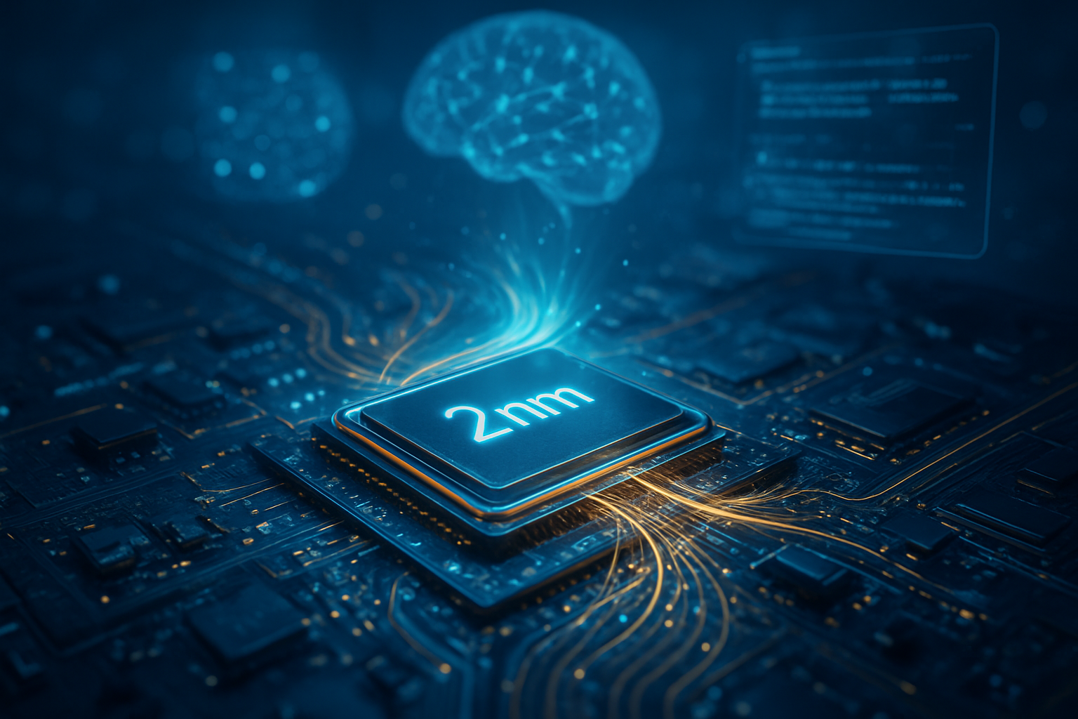
Taiwan Semiconductor Manufacturing Co. (NYSE: TSM) has shattered financial records, reporting a net profit of US$16 billion for the fourth quarter of 2025—a 35% year-over-year increase. The blowout results were driven by unrelenting demand for AI accelerators and the rapid ramp-up of 3nm and 5nm technologies, which now account for 63% of the company's total wafer revenue. CEO C.C. Wei confirmed that the 'AI gold rush' continues to fuel high utilization rates across all advanced fabs, solidifying TSMC's role as the indispensable backbone of the global AI economy.
The financial surge marks a historic milestone for the foundry giant, as revenue from High-Performance Computing (HPC) and AI applications now officially accounts for 55% of the company's total intake, significantly outpacing the smartphone segment for the first time. As the world transitions into a new era of generative AI, TSMC’s quarterly performance serves as a primary bellwether for the entire tech sector, signaling that the infrastructure build-out for artificial intelligence is accelerating rather than cooling off.
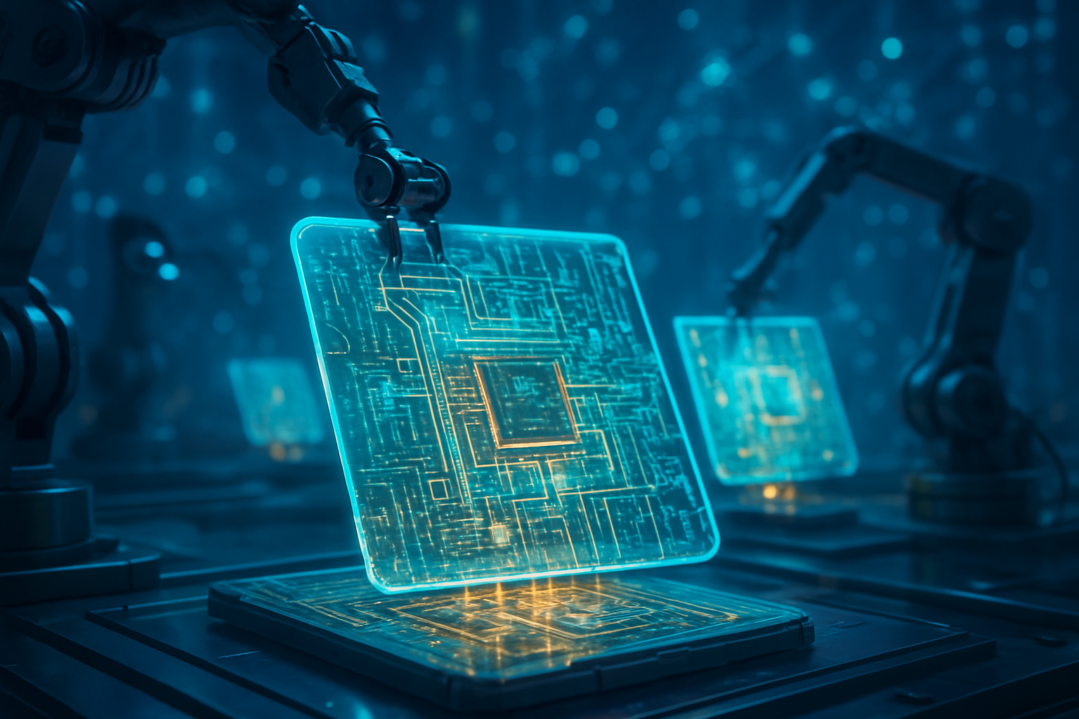
Scaling the Silicon Frontier: 3nm Dominance and the CoWoS Breakthrough
At the heart of TSMC’s record-breaking quarter is the massive commercial success of its N3 (3nm) and N5 (5nm) process nodes. The 3nm family alone contributed 28% of total wafer revenue in Q4 2025, a steep climb from previous quarters as major clients migrated their flagship products to the more efficient node. This transition represents a significant technical leap over the 5nm generation, offering up to 15% better performance at the same power levels or a 30% reduction in power consumption. These specifications have become critical for AI data centers, where energy efficiency is the primary constraint on scaling massive LLM (Large Language Model) clusters.
Beyond traditional wafer fabrication, TSMC has successfully navigated the "packaging crunch" that plagued the industry throughout 2024. The company’s Chip-on-Wafer-on-Substrate (CoWoS) advanced packaging capacity—a prerequisite for high-bandwidth memory integration in AI chips—has doubled over the last year to approximately 80,000 wafers per month. This expansion has been vital for the delivery of next-generation accelerators like the Blackwell series from NVIDIA (NASDAQ: NVDA). Industry experts note that TSMC’s ability to integrate advanced lithography with sophisticated 3D packaging is what currently separates it from competitors like Samsung and Intel (NASDAQ: INTC).
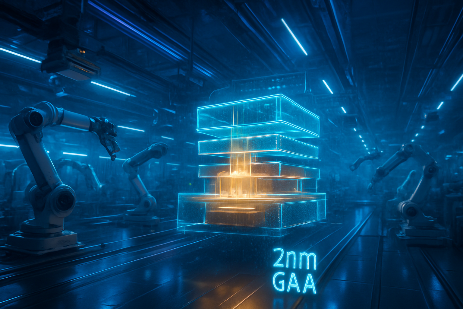
The quarter also saw the official commencement of 2nm (N2) mass production at TSMC’s Hsinchu and Kaohsiung facilities. Unlike the FinFET transistors used in previous nodes, the 2nm process utilizes Nanosheet (GAAFET) architecture, allowing for finer control over current flow and further reducing leakage. Initial yields are reportedly ahead of schedule, with research analysts suggesting that the "AI gold rush" has provided TSMC with the necessary capital to accelerate this transition faster than any previous node shift in the company's history.
The Kingmaker: Impact on Big Tech and the Fabless Ecosystem
TSMC’s dominance has created a unique market dynamic where the company acts as the ultimate gatekeeper for the AI industry. Major clients, including NVIDIA, Apple (NASDAQ: AAPL), and Advanced Micro Devices (NASDAQ: AMD), are currently in a high-stakes competition to secure "golden wafers" for 2026 and 2027. NVIDIA, which is projected to become TSMC’s largest customer by revenue in the coming year, has reportedly secured nearly 60% of all available CoWoS output for its upcoming Rubin architecture, leaving rivals and hyperscalers to fight for the remaining capacity.
This supply-side dominance provides a strategic advantage to "Early Adopters" like Apple, which has utilized its massive capital reserves to lock in 2nm capacity for its upcoming A19 and M5 chips. For smaller AI startups and specialized chipmakers, the barrier to entry is rising. With TSMC’s advanced node capacity essentially pre-sold through 2027, the "haves" of the AI world—those with established TSMC allocations—are pulling further ahead of the "have-nots." This has led to a surge in strategic partnerships and long-term supply agreements as companies seek to avoid the crippling shortages seen in early 2024.
The competitive landscape is also shifting for TSMC’s foundry rivals. While Intel has made strides with its 18A node, TSMC’s Q4 results suggest that the scale of its ecosystem remains its greatest moat. The "Foundry 2.0" model, as CEO C.C. Wei describes it, integrates manufacturing, advanced packaging, and testing into a single, seamless pipeline. This vertical integration has made it difficult for competitors to lure away high-margin AI clients who require the guaranteed reliability of TSMC’s proven high-volume manufacturing.
The Backbone of the Global AI Economy
TSMC’s $16 billion profit is more than just a corporate success story; it is a reflection of the broader geopolitical and economic significance of semiconductors in 2026. The shift in revenue mix toward HPC/AI underscores the reality that "Sovereign AI"—nations building their own localized AI infrastructure—is becoming a primary driver of global demand. From the United States to Europe and the Middle East, governments are subsidizing data center builds that rely almost exclusively on the silicon produced in TSMC’s Taiwan-based fabs.
The wider significance of this milestone also touches on the environmental impact of AI. As the industry faces criticism over the energy consumption of data centers, the rapid adoption of 3nm and the impending move to 2nm are seen as the only viable path to sustainable AI. By packing more transistors into the same area with lower voltage requirements, TSMC is effectively providing the "efficiency dividends" necessary to keep the AI revolution from overwhelming global power grids. This technical necessity has turned TSMC into a critical pillar of global ESG goals, even as its own power consumption rises to meet production demands.
Comparisons to previous AI milestones are striking. While the release of ChatGPT in 2022 was the "software moment" for AI, TSMC’s Q4 2025 results mark the "hardware peak." The sheer volume of capital being funneled into advanced nodes suggests that the industry has moved past the experimental phase and is now in a period of heavy industrialization. Unlike the "dot-com" bubble, this era is characterized by massive, tangible hardware investments that are already yielding record profits for the infrastructure providers.
The Road to 1.6nm: What Lies Ahead
Looking toward the future, the momentum shows no signs of slowing. TSMC has already announced a massive capital expenditure budget of $52–$56 billion for 2026, aimed at further expanding its footprint in Arizona, Japan, and Germany. The focus is now shifting toward the A16 (1.6nm) process, which is slated for volume production in the second half of 2026. This node will introduce "Super Power Rail" technology—a backside power delivery system that decouples power routing from signal routing, significantly boosting efficiency and performance for AI logic.
Experts predict that the next major challenge for TSMC will be managing the "complexity wall." As transistors shrink toward the atomic scale, the cost of design and manufacturing continues to skyrocket. This may lead to a more modular future, where "chiplets" from different process nodes are combined using TSMC’s SoIC (System-on-Integrated-Chips) technology. This would allow customers to use expensive 2nm logic only where necessary, while utilizing 5nm or 7nm for less critical components, potentially easing the demand on the most advanced nodes.
Furthermore, the integration of silicon photonics into the packaging process is expected to be the next major breakthrough. As AI models grow, the bottleneck is no longer just how fast a chip can think, but how fast chips can talk to each other. TSMC’s research into CPO (Co-Packaged Optics) is expected to reach commercial viability by late 2026, potentially enabling a 10x increase in data transfer speeds between AI accelerators.
Conclusion: A New Era of Silicon Supremacy
TSMC’s Q4 2025 earnings represent a definitive statement: the AI era is not a speculative bubble, but a fundamental restructuring of the global technology landscape. By delivering a $16 billion profit and scaling 3nm and 5nm nodes to dominate 63% of its revenue, the company has proven that it is the heartbeat of modern computing. CEO C.C. Wei’s "AI gold rush" is more than a metaphor; it is a multi-billion dollar reality that is reshaping every industry from healthcare to high finance.
As we move further into 2026, the key metrics to watch will be the 2nm ramp-up and the progress of TSMC’s overseas expansion. While geopolitical tensions remain a constant background noise, the world’s total reliance on TSMC’s advanced nodes has created a "silicon shield" that makes the company’s stability a matter of global economic security. For now, TSMC stands alone at the top of the mountain, the essential architect of the intelligence age.
This content is intended for informational purposes only and represents analysis of current AI developments.
TokenRing AI delivers enterprise-grade solutions for multi-agent AI workflow orchestration, AI-powered development tools, and seamless remote collaboration platforms.
For more information, visit https://www.tokenring.ai/.