Tag: TSMC

  • The 2,048-Bit Breakthrough: SK Hynix and Samsung Launch a New Era of Generative AI with HBM4

    The 2,048-Bit Breakthrough: SK Hynix and Samsung Launch a New Era of Generative AI with HBM4

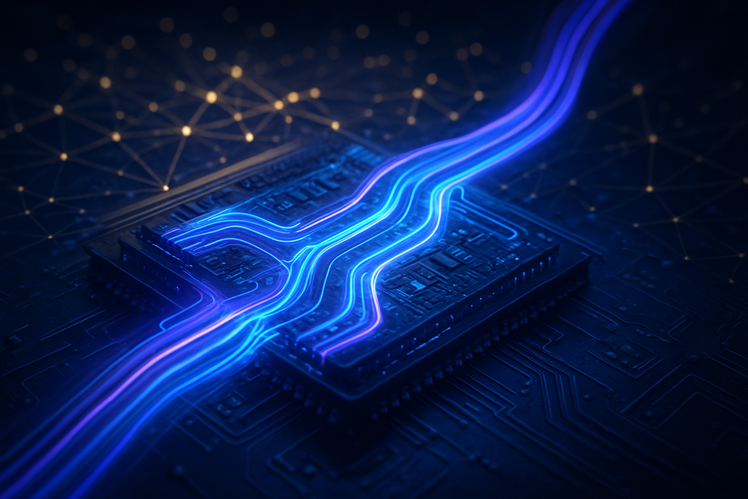
    As of January 13, 2026, the artificial intelligence industry has reached a pivotal juncture in its hardware evolution. The "Memory Wall"—the performance gap between ultra-fast processors and the memory that feeds them—is finally being dismantled. This week marks a definitive shift as SK Hynix (KRX: 000660) and Samsung Electronics (KRX: 005930) move into high-gear production of HBM4, the next generation of High Bandwidth Memory. This transition isn't just an incremental update; it is a fundamental architectural redesign centered on a new 2,048-bit interface that promises to double the data throughput available to the world’s most powerful generative AI models.

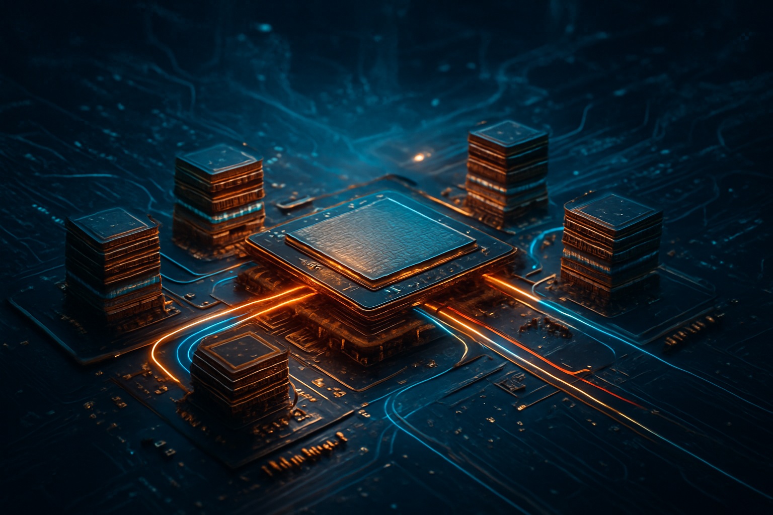
    The immediate significance of this development cannot be overstated. As large language models (LLMs) push toward multi-trillion parameter scales, the bottleneck has shifted from raw compute power to memory bandwidth. HBM4 provides the essential "oxygen" for these massive models to breathe, offering per-stack bandwidth of up to 2.8 TB/s. With major players like NVIDIA (NASDAQ: NVDA) and AMD (NASDAQ: AMD) integrating these stacks into their 2026 flagship accelerators, the race for HBM4 dominance has become the most critical subplot in the global AI arms race, determining which hardware platforms will lead the next decade of autonomous intelligence.

    The Technical Leap: Doubling the Highway

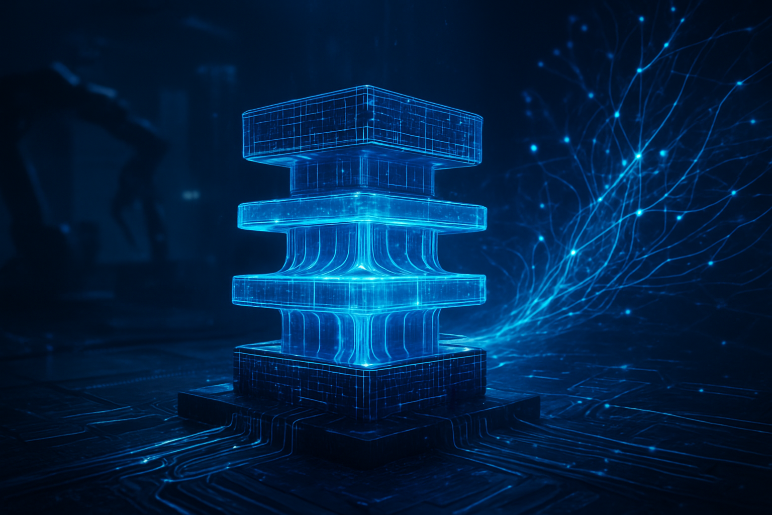
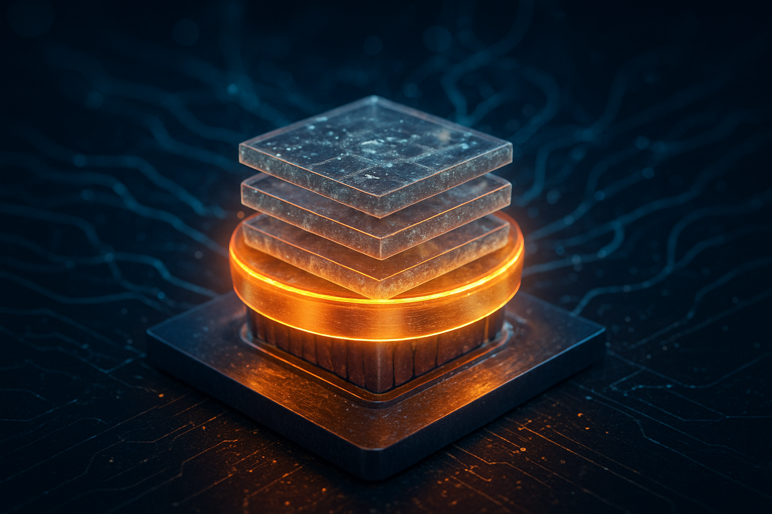
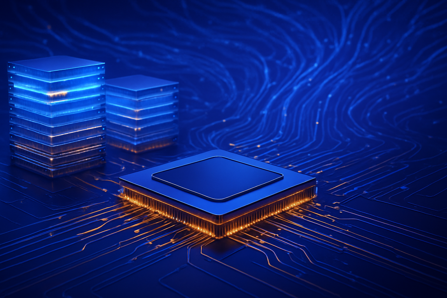
    The move to HBM4 represents the most significant technical overhaul in the history of memory. For the first time, the industry is transitioning from a 1,024-bit interface—a standard that held firm through HBM2 and HBM3—to a massive 2,048-bit interface. By doubling the number of I/O pins, manufacturers can achieve unprecedented data transfer speeds while actually reducing the clock speed and power consumption per bit. This architectural shift is complemented by the transition to 16-high (16-Hi) stacking, allowing for individual memory stacks with capacities ranging from 48GB to 64GB.

    Another groundbreaking technical change in HBM4 is the introduction of a logic base die manufactured on advanced foundry nodes. Previously, HBM base dies were built using standard DRAM processes. However, HBM4 requires the foundation of the stack to be a high-performance logic chip. SK Hynix has partnered with TSMC (NYSE: TSM) to utilize their 5nm and 12nm nodes for these base dies, allowing for "Custom HBM" where AI-specific controllers are integrated directly into the memory. Samsung, meanwhile, is leveraging its internal "one-stop shop" advantage, using its own 4nm foundry process to create a vertically integrated solution that promises lower latency and improved thermal management.

    The packaging techniques used to assemble these 16-layer skyscrapers are equally sophisticated. SK Hynix is employing an advanced version of its Mass Reflow Molded Underfill (MR-MUF) technology, thinning wafers to a mere 30 micrometers to keep the entire stack within the JEDEC-specified height limits. Samsung is aggressively pivoting toward Hybrid Bonding (copper-to-copper direct contact), a method that eliminates traditional micro-bumps. Industry experts suggest that Hybrid Bonding could be the "holy grail" for HBM4, as it significantly reduces thermal resistance—a critical factor for GPUs like NVIDIA’s upcoming Rubin platform, which are expected to exceed 1,000W in power draw.

    The Corporate Duel: Strategic Alliances and Vertical Integration

    The competitive landscape of 2026 has bifurcated into two distinct strategic philosophies. SK Hynix, which currently holds a market share lead of roughly 55%, has doubled down on its "Trilateral Alliance" with TSMC and NVIDIA. By outsourcing the logic die to TSMC, SK Hynix has effectively tethered its success to the world’s leading foundry and its primary customer. This ecosystem-centric approach has allowed them to remain the preferred vendor for NVIDIA's Blackwell and now the newly unveiled "Rubin" (R100) architecture, which features eight stacks of HBM4 for a staggering 22 TB/s of aggregate bandwidth.

    Samsung Electronics, however, is executing a "turnkey" strategy aimed at disrupting the status quo. By handling the DRAM fabrication, logic die manufacturing, and advanced 3D packaging all under one roof, Samsung aims to offer better price-to-performance ratios and faster customization for bespoke AI silicon. This strategy bore major fruit early this year with a reported $16.5 billion deal to supply Tesla (NASDAQ: TSLA) with HBM4 for its next-generation Dojo supercomputer chips. While Samsung struggled during the HBM3e era, its early lead in Hybrid Bonding and internal foundry capacity has positioned it as a formidable challenger to the SK Hynix-TSMC hegemony.

    Micron Technology (NASDAQ: MU) also remains a key player, focusing on high-efficiency HBM4 designs for the enterprise AI market. While smaller in scale compared to the South Korean giants, Micron’s focus on power-per-watt has earned it significant slots in AMD’s new Helios (Instinct MI455X) accelerators. The battle for market positioning is no longer just about who can make the most chips, but who can offer the most "customizable" memory. As hyperscalers like Amazon and Google design their own AI chips (TPUs and Trainium), the ability for memory makers to integrate specific logic functions into the HBM4 base die has become a critical strategic advantage.

    The Global AI Landscape: Breaking the Memory Wall

    The arrival of HBM4 is a milestone that reverberates far beyond the semiconductor industry; it is a prerequisite for the next stage of AI democratization. Until now, the high cost and limited availability of high-bandwidth memory have concentrated the most advanced AI capabilities within a handful of well-funded labs. By providing a 2x leap in bandwidth and capacity, HBM4 enables more efficient training of "Sovereign AI" models and allows smaller data centers to run more complex inference tasks. This fits into the broader trend of AI shifting from experimental research to ubiquitous infrastructure.

    However, the transition to HBM4 also brings concerns regarding the environmental footprint of AI. While the 2,048-bit interface is more efficient on a per-bit basis, the sheer density of these 16-layer stacks creates immense thermal challenges. The move toward liquid-cooled data centers is no longer an option but a requirement for 2026-era hardware. Comparison with previous milestones, such as the introduction of HBM1 in 2013, shows just how far the industry has come: HBM4 offers nearly 20 times the bandwidth of its earliest ancestor, reflecting the exponential growth in demand fueled by the generative AI explosion.

    Potential disruption is also on the horizon for traditional server memory. As HBM4 becomes more accessible and customizable, we are seeing the beginning of the "Memory-Centric Computing" era, where processing is moved closer to the data. This could eventually threaten the dominance of standard DDR5 memory in high-performance computing environments. Industry analysts are closely watching whether the high costs of HBM4 production—estimated to be several times that of standard DRAM—will continue to be absorbed by the high margins of the AI sector or if they will eventually lead to a cooling of the current investment cycle.

    Future Horizons: Toward HBM4e and Beyond

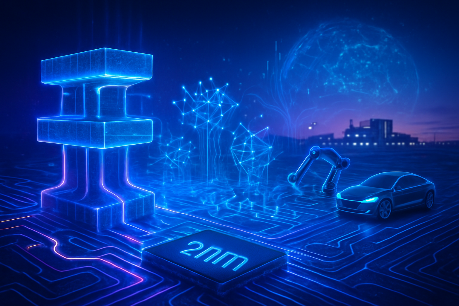
    Looking ahead, the roadmap for memory is already stretching toward the end of the decade. Near-term, we expect to see the announcement of HBM4e (Enhanced) by late 2026, which will likely push pin speeds toward 14 Gbps and expand stack heights even further. The successful implementation of Hybrid Bonding will be the gateway to HBM5, where we may see the total merging of logic and memory layers into a single, monolithic 3D structure. Experts predict that by 2028, we will see "In-Memory Processing" where simple AI calculations are performed within the HBM stack itself, further reducing latency.

    The applications on the horizon are equally transformative. With the massive memory capacity afforded by HBM4, the industry is moving toward "World Models" that can process hours of high-resolution video or massive scientific datasets in a single context window. However, challenges remain—particularly in yield rates for 16-high stacks and the geopolitical complexities of the semiconductor supply chain. Ensuring that HBM4 production can scale to meet the demand of the "Agentic AI" era, where millions of autonomous agents will require constant memory access, will be the primary task for engineers over the next 24 months.

    Conclusion: The Backbone of the Intelligent Era

    In summary, the HBM4 race is the definitive battleground for the next phase of the AI revolution. SK Hynix’s collaborative ecosystem and Samsung’s vertically integrated "one-stop shop" represent two distinct paths toward solving the same fundamental problem: the insatiable need for data speed. The shift to a 2,048-bit interface and the integration of logic dies mark the point where memory ceased to be a passive storage medium and became an active, intelligent component of the AI processor itself.

    As we move through 2026, the success of these companies will be measured by their ability to achieve high yields in the difficult 16-layer assembly process and their capacity to innovate in thermal management. This development will likely be remembered as the moment the "Memory Wall" was finally breached, enabling a new generation of AI models that are faster, more capable, and more efficient than ever before. Investors and tech enthusiasts should keep a close eye on the Q1 and Q2 earnings reports of the major players, as the first volume shipments of HBM4 begin to reshape the financial and technological landscape of the AI industry.


    This content is intended for informational purposes only and represents analysis of current AI developments.

    TokenRing AI delivers enterprise-grade solutions for multi-agent AI workflow orchestration, AI-powered development tools, and seamless remote collaboration platforms.
    For more information, visit https://www.tokenring.ai/.

  • The High-NA Revolution: Inside the $400 Million Machines Defining the Angstrom Era

    The High-NA Revolution: Inside the $400 Million Machines Defining the Angstrom Era

    The global race for artificial intelligence supremacy has officially entered its most expensive and physically demanding chapter yet. As of early 2026, the transition from experimental R&D to high-volume manufacturing (HVM) for High-Numerical Aperture (High-NA) Extreme Ultraviolet (EUV) lithography is complete. These massive, $400 million machines, manufactured exclusively by ASML (NASDAQ: ASML), have become the literal gatekeepers of the "Angstrom Era," enabling the production of transistors so small that they are measured by the width of individual atoms.

    The arrival of High-NA EUV is not merely an incremental upgrade; it is a critical pivot point for the entire AI industry. As Large Language Models (LLMs) scale toward 100-trillion parameter architectures, the demand for more energy-efficient and dense silicon has made traditional lithography obsolete. Without the precision afforded by High-NA, the hardware required to sustain the current pace of AI development would hit a "thermal wall," where energy consumption and heat dissipation would outpace any gains in raw processing power.

    The Optical Engineering Marvel: 0.55 NA and the End of Multi-Patterning

    At the heart of this revolution is the ASML Twinscan EXE:5200 series. The "High-NA" designation refers to the increase in numerical aperture from 0.33 to 0.55. In the world of optics, a higher NA allows the lens system to collect more light and achieve a finer resolution. For chipmakers, this means the ability to print features as small as 8nm, a significant leap from the 13nm limit of previous-generation EUV tools. This increased resolution enables a nearly 3-fold increase in transistor density, allowing engineers to cram more logic and memory into the same square millimeter of silicon.

    The most immediate technical benefit for foundries is the return to "single-patterning." In the previous sub-3nm era, manufacturers were forced to use complex "multi-patterning" techniques—essentially printing a single layer of a chip across multiple exposures—to bypass the resolution limits of 0.33 NA machines. This process was notoriously error-prone, time-consuming, and decimated yields. The High-NA systems allow for these intricate designs to be printed in a single pass, slashing the number of critical layer process steps from over 40 to fewer than 10. This efficiency is what makes the 1.4nm (Intel 14A) and upcoming 1nm nodes economically viable.

    Initial reactions from the semiconductor research community have been a mix of awe and cautious pragmatism. While the technical capabilities of the EXE:5200B are undisputed—boasting a throughput of over 200 wafers per hour and sub-nanometer overlay accuracy—the sheer scale of the hardware has presented logistical nightmares. These machines are roughly the size of a double-decker bus and weigh 150,000 kilograms, requiring cleanrooms with reinforced flooring and specialized ceiling heights that many older fabs simply cannot accommodate.

    The Competitive Tectonic Shift: Intel’s Lead and the Foundries' Dilemma

    The deployment of High-NA has created a stark strategic divide among the world’s leading chipmakers. Intel (NASDAQ: INTC) has emerged as the early winner in this transition, having successfully completed acceptance testing for its first high-volume EXE:5200B system in Oregon this month. By being the "First Mover," Intel is leveraging High-NA to underpin its Intel 14A node, aiming to reclaim the title of process leadership from its rivals. This aggressive stance is a cornerstone of Intel Foundry's strategy to attract external customers like NVIDIA (NASDAQ: NVDA) and Microsoft (NASDAQ: MSFT) who are desperate for the most advanced AI silicon.

    In contrast, TSMC (NYSE: TSM) has adopted a "calculated delay" strategy. The Taiwanese giant has spent the last year optimizing its A16 (1.6nm) node using older 0.33 NA machines with sophisticated multi-patterning to maintain its industry-leading yields. However, TSMC is not ignoring the future; the company has reportedly secured an massive order of nearly 70 High-NA machines for its A14 and A10 nodes slated for 2027 and beyond. This creates a fascinating competitive window where Intel may have a technical density advantage, while TSMC maintains a volume and cost-efficiency lead.

    Meanwhile, Samsung (KRX: 005930) is attempting a high-stakes "leapfrog" maneuver. After integrating its first High-NA units for 2nm production, internal reports suggest the company may skip the 1.4nm node entirely to focus on a "dream" 1nm process. This strategic pivot is intended to close the gap with TSMC by betting on the ultimate physical limit of silicon earlier than its competitors. For AI labs and chip designers, this means the next three years will be defined by which foundry can most effectively balance the astronomical costs of High-NA with the performance demands of next-gen Blackwell and Rubin-class GPUs.

    Moore's Law and the "2-Atom Wall"

    The wider significance of High-NA EUV lies in its role as the ultimate life-support system for Moore’s Law. We are no longer just fighting the laws of economics; we are fighting the laws of physics. At the 1.4nm and 1nm levels, we are approaching what researchers call the "2-atom wall"—a point where transistor features are only two atoms thick. Beyond this, traditional silicon faces insurmountable challenges from quantum tunneling, where electrons literally jump through barriers they are supposed to be blocked by, leading to massive data errors and power leakage.

    High-NA is being used in tandem with other radical architectures to circumvent these limits. Technologies like Backside Power Delivery (which Intel calls PowerVia) move the power lines to the back of the wafer, freeing up space on the front for even denser transistor placement. This synergy is what allows for the power-efficiency gains required for the next generation of "Physical AI"—autonomous robots and edge devices that need massive compute power without being tethered to a power plant.

    However, the concentration of this technology in the hands of a single supplier, ASML, and three primary customers raises significant concerns about the democratization of AI. The $400 million price tag per machine, combined with the billions required for fab construction, creates a barrier to entry that effectively locks out any new players in the leading-edge foundry space. This consolidation ensures that the "AI haves" and "AI have-nots" will be determined by who has the deepest pockets and the most stable supply chains for Dutch-made optics.

    The Horizon: Hyper-NA and the Sub-1nm Future

    As the industry digests the arrival of High-NA, ASML is already looking toward the next frontier: Hyper-NA. With a projected numerical aperture of 0.75, Hyper-NA systems (likely the HXE series) are already on the roadmap for 2030. These machines will be necessary to push manufacturing into the sub-10-Angstrom (sub-1nm) range. However, experts predict that Hyper-NA will face even steeper challenges, including "polarization death," where the angles of light become so extreme that they cancel each other out, requiring entirely new types of polarization filters.

    In the near term, the focus will shift from "can we print it?" to "can we yield it?" The industry is expected to see a surge in the use of AI-driven metrology and inspection tools to manage the extreme precision required by High-NA. We will also likely see a major shift in material science, with researchers exploring 2D materials like molybdenum disulfide to replace silicon as we hit the 2-atom wall. The chips powering the AI models of 2028 and beyond will likely look nothing like the processors we use today.

    Conclusion: A Tectonic Moment in Computing History

    The successful deployment of ASML’s High-NA EUV tools marks one of the most significant milestones in the history of the semiconductor industry. It represents the pinnacle of human engineering—using light to manipulate matter at the near-atomic scale. For the AI industry, this is the infrastructure that makes the "Sovereign AI" dreams of nations and the "AGI" goals of labs possible.

    The key takeaways for the coming year are clear: Intel has secured a narrow but vital head start in the Angstrom era, while TSMC remains the formidable incumbent betting on refined execution. The massive capital expenditure required for these tools will likely drive up the price of high-end AI chips, but the performance and efficiency gains will be the engine that drives the next decade of digital transformation. Watch closely for the first 1.4nm "tape-outs" from major AI players in the second half of 2026; they will be the first true test of whether the $400 million gamble has paid off.


    This content is intended for informational purposes only and represents analysis of current AI developments.

    TokenRing AI delivers enterprise-grade solutions for multi-agent AI workflow orchestration, AI-powered development tools, and seamless remote collaboration platforms.
    For more information, visit https://www.tokenring.ai/.

  • The GAA Era Arrives: TSMC Enters Mass Production of 2nm Chips to Fuel the Next AI Supercycle

    The GAA Era Arrives: TSMC Enters Mass Production of 2nm Chips to Fuel the Next AI Supercycle

    As the calendar turns to early 2026, the global semiconductor landscape has officially shifted on its axis. Taiwan Semiconductor Manufacturing Company (NYSE:TSM), commonly known as TSMC, has successfully crossed the finish line of its most ambitious technological transition in a decade. Following a rigorous ramp-up period that concluded in late 2025, the company’s 2nm (N2) node is now in high-volume manufacturing, ushering in the era of Gate-All-Around (GAA) nanosheet transistors. This milestone marks more than just a reduction in feature size; it represents the foundational infrastructure upon which the next generation of generative AI and high-performance computing (HPC) will be built.

    The immediate significance of this development cannot be overstated. By moving into volume production ahead of its most optimistic competitors and maintaining superior yield rates, TSMC has effectively secured its position as the primary engine of the AI economy. With primary production hubs at Fab 22 in Kaohsiung and Fab 20 in Hsinchu reaching a combined output of over 50,000 wafers per month this January, the company is already churning out the silicon that will power the most advanced smartphones and data center accelerators of 2026 and 2027.

    The Nanosheet Revolution: Engineering the Future of Silicon

    The N2 node represents a fundamental departure from the FinFET (Fin Field-Effect Transistor) architecture that has dominated the industry for the last several process generations. In traditional FinFETs, the gate controls the channel on three sides; however, as transistors shrink toward the 2nm threshold, current leakage becomes an insurmountable hurdle. TSMC’s shift to Gate-All-Around (GAA) nanosheet transistors solves this by wrapping the gate around all four sides of the channel, providing superior electrostatic control and drastically reducing power leakage.

    Technical specifications for the N2 node are staggering. Compared to the previous 3nm (N3E) process, the 2nm node offers a 10% to 15% increase in performance at the same power envelope, or a significant 25% to 30% reduction in power consumption at the same clock speed. Furthermore, the N2 node introduces "Super High-Performance Metal-Insulator-Metal" (SHPMIM) capacitors. These components double the capacitance density while cutting resistance by 50%, a critical advancement for AI chips that must handle massive, instantaneous power draws without losing efficiency. Early logic test chips have reportedly achieved yield rates between 70% and 80%, a metric that validates TSMC's manufacturing prowess compared to the more volatile early yields seen in rival GAA implementations.

    A High-Stakes Duel: Intel, Samsung, and the Battle for Foundry Supremacy

    The successful ramp of N2 has profound implications for the competitive balance between the "Big Three" chipmakers. While Samsung Electronics (KRX:005930) was technically the first to move to GAA at the 3nm stage, its yields have historically struggled to compete with the stability of TSMC. Samsung’s recent launch of the SF2 node and the Exynos 2600 chip shows progress, but the company remains primarily a secondary source for major designers. Meanwhile, Intel (NASDAQ:INTC) has emerged as a formidable challenger with its 18A node. Intel’s 18A utilizes "PowerVia" (Backside Power Delivery), a technology TSMC will not integrate until its N2P variant in late 2026. This gives Intel a temporary technical lead in raw power delivery metrics, even as TSMC maintains a superior transistor density of roughly 313 million transistors per square millimeter.

    For the world’s most valuable tech giants, the arrival of N2 is a strategic windfall. Apple (NASDAQ:AAPL), acting as TSMC’s "alpha" customer, has reportedly secured over 50% of the initial 2nm capacity to power its upcoming iPhone 18 series and the M5/M6 Mac silicon. Close on their heels is Nvidia (NASDAQ:NVDA), which is leveraging the N2 node for its next-generation AI platforms succeeding the Blackwell architecture. Other major players including Advanced Micro Devices (NASDAQ:AMD), Broadcom (NASDAQ:AVGO), and MediaTek (TPE:2454) have already finalized their 2026 production slots, signaling a collective industry bet that TSMC’s N2 will be the gold standard for efficiency and scale.

    Scaling AI: The Broader Landscape of 2nm Integration

    The transition to 2nm is inextricably linked to the trajectory of artificial intelligence. As Large Language Models (LLMs) grow in complexity, the demand for "compute" has become the defining constraint of the tech industry. The 25-30% power savings offered by N2 are not merely a luxury for mobile devices; they are a survival necessity for data centers. By reducing the energy required per inference or training cycle, 2nm chips allow hyperscalers like Microsoft (NASDAQ:MSFT) and Amazon (NASDAQ:AMZN) to pack more density into their existing power footprints, potentially slowing the skyrocketing environmental costs of the AI boom.

    This milestone also reinforces the "Moore's Law is not dead" narrative, albeit with a caveat: while transistor density continues to increase, the cost per transistor is rising. The complexity of GAA manufacturing requires multi-billion dollar investments in Extreme Ultraviolet (EUV) lithography and specialized cleanrooms. This creates a widening "innovation gap" where only the largest, most capitalized companies can afford the leap to 2nm, potentially consolidating power within a handful of AI leaders while leaving smaller startups to rely on older, less efficient silicon.

    The Roadmap Beyond: A16 and the 1.6nm Frontier

    The arrival of 2nm mass production is just the beginning of a rapid-fire roadmap. TSMC has already disclosed that its N2P node—the enhanced version of 2nm featuring Backside Power Delivery—is on track for mass production in late 2026. This will be followed closely by the A16 node (1.6nm) in 2027, which will incorporate "Super PowerRail" technology to further optimize power distribution directly to the transistor's source and drain.

    Experts predict that the next eighteen months will focus on "advanced packaging" as much as the nodes themselves. Technologies like CoWoS (Chip on Wafer on Substrate) will be essential to combine 2nm logic with high-bandwidth memory (HBM4) to create the massive AI "super-chips" of the future. The challenge moving forward will be heat dissipation; as transistors become more densely packed, managing the thermal output of these 2nm dies will require innovative liquid cooling and material science breakthroughs.

    Conclusion: A Pivot Point for the Digital Age

    TSMC’s successful transition to the 2nm N2 node in early 2026 stands as one of the most significant engineering feats of the decade. By navigating the transition from FinFET to GAA nanosheets while maintaining industry-leading yields, the company has solidified its role as the indispensable foundation of the AI era. While Intel and Samsung continue to provide meaningful competition, TSMC’s ability to scale this technology for giants like Apple and Nvidia ensures that the heartbeat of global innovation remains centered in Taiwan.

    In the coming months, the industry will watch closely as the first 2nm consumer devices hit the shelves and the first N2-based AI clusters go online. This development is more than a technical upgrade; it is the starting gun for a new epoch of computing performance, one that will determine the pace of AI advancement for years to come.


    This content is intended for informational purposes only and represents analysis of current AI developments.

    TokenRing AI delivers enterprise-grade solutions for multi-agent AI workflow orchestration, AI-powered development tools, and seamless remote collaboration platforms.
    For more information, visit https://www.tokenring.ai/.

  • The Silicon Sustainability Crisis: Inside the Multi-Billion Dollar Push for ‘Green Fabs’ in 2026

    The Silicon Sustainability Crisis: Inside the Multi-Billion Dollar Push for ‘Green Fabs’ in 2026

    As of January 2026, the artificial intelligence revolution has reached a critical paradox. While AI is being hailed as the ultimate tool to solve the climate crisis, the physical infrastructure required to build it—massive semiconductor manufacturing plants known as "mega-fabs"—has become one of the world's most significant environmental challenges. The explosive demand for next-generation AI chips from companies like NVIDIA (NASDAQ:NVDA) is forcing the world’s three largest chipmakers to fundamentally redesign the "factory of the future."

    Intel (NASDAQ:INTC), TSMC (NYSE:TSM), and Samsung (KRX:005930) are currently locked in a high-stakes race to build "Green Fabs." These multi-billion dollar facilities, located from the deserts of Arizona to the plains of Ohio and the industrial hubs of South Korea, are no longer just measured by their nanometer precision. In 2026, the primary metrics for success have shifted to "Net-Zero Liquid Discharge" and "24/7 Carbon-Free Energy." This shift marks a historic turning point where environmental sustainability is no longer a corporate social responsibility (CSR) footnote but a core requirement for high-volume manufacturing.

    The Technical Toll of 2nm: Powering the High-NA EUV Era

    The push for Green Fabs is driven by the extreme technical requirements of the latest chip nodes. To produce the 2nm and sub-2nm chips required for 2026-era AI models, manufacturers must use High-NA (Numerical Aperture) Extreme Ultraviolet (EUV) lithography machines produced by ASML (NASDAQ:ASML). These machines are engineering marvels but energy gluttons; a single High-NA EUV unit (such as the EXE:5200) consumes approximately 1.4 megawatts of electricity—enough to power over a thousand homes. When a single mega-fab houses dozens of these machines, the power demand rivals that of a mid-sized city.

    To mitigate this, the "Big Three" are deploying radical new efficiency technologies. Samsung recently announced a partnership with NVIDIA to deploy "Autonomous Digital Twins" across its Taylor, Texas facility. This system uses tens of thousands of sensors and AI-driven simulations to optimize airflow and chemical delivery in real-time, reportedly improving energy efficiency by 20% compared to 2024 standards. Meanwhile, Intel is experimenting with hydrogen recovery systems in its upcoming Magdeburg, Germany site, capturing and reusing the hydrogen gas used during the lithography process to generate supplemental on-site power.

    Water scarcity has become the second technical hurdle. In Arizona, TSMC has pioneered a 15-acre Industrial Water Reclamation Plant (IWRP) that aims for a 90% recycling rate. This "closed-loop" system ensures that nearly every gallon of water used to wash silicon wafers is treated and returned to the cleanroom, leaving only evaporation as a source of loss. This is a massive leap from a decade ago, when semiconductor manufacturing was notorious for depleting local aquifers and discharging chemical-heavy wastewater.

    The Nuclear Renaissance and the Power Struggle for the Grid

    The sheer scale of energy required for AI chip production has sparked a "nuclear renaissance" in the semiconductor industry. In late 2025, Samsung C&T signed landmark agreements with Small Modular Reactor (SMR) pioneers like NuScale and X-energy. By early 2026, the strategy is clear: because solar and wind cannot provide the 24/7 "baseload" power required for a fab that never sleeps, chipmakers are turning to dedicated nuclear solutions. This move is supported by tech giants like Microsoft (NASDAQ:MSFT) and Amazon (NASDAQ:AMZN), who have recently secured nearly 6 gigawatts of nuclear power to ensure the fabs and data centers they rely on remain carbon-neutral.

    However, this hunger for power has led to unprecedented corporate friction. In a notable incident in late 2025, Meta (NASDAQ:META) reportedly petitioned Ohio regulators to reassign 200 megawatts of power capacity originally reserved for Intel’s New Albany mega-fab. Meta argued that because Intel’s high-volume production had been delayed to 2030, the power would be better used for Meta’s nearby AI data centers. This "power grab" highlights a growing tension: as the world transitions to green energy, the supply of stable, renewable power is becoming a more significant bottleneck than silicon itself.

    For startups and smaller AI labs, the emergence of Green Fabs creates a two-tiered market. Companies that can afford to pay the premium for "Green Silicon" will see their ESG (Environmental, Social, and Governance) scores soar, making them more attractive to institutional investors. Conversely, those relying on older, "dirtier" fabs may find themselves locked out of certain markets or facing carbon taxes that erode their margins.

    Environmental Justice and the Global Landscape

    The transition to Green Fabs is also a response to growing geopolitical and social pressure. In Taiwan, TSMC has faced recurring droughts that threatened both chip production and local agriculture. By investing in 100% renewable energy and advanced water recycling, TSMC is not just being "green"—it is ensuring its survival in a region where resources are increasingly contested. Similarly, Intel’s "Net-Positive Water" goal for its Ohio site involves funding massive wetland restoration projects, such as the Dillon Lake initiative, to balance its environmental footprint.

    Critics, however, point to a "structural sustainability risk" in the way AI chips are currently made. The demand for High-Bandwidth Memory (HBM), essential for AI GPUs, has led to a "stacking loss" crisis. In early 2026, the complexity of 16-high HBM stacks has resulted in lower yields, meaning a significant amount of silicon and energy is wasted on defective chips. Industry experts argue that until yields improve, the "greenness" of a fab is partially offset by the waste generated in the pursuit of extreme performance.

    This development fits into a broader trend where the "hidden costs" of AI are finally being accounted for. Much like the transition from coal to renewables in the 2010s, the semiconductor industry is realizing that the old model of "performance at any cost" is no longer viable. The Green Fab movement is the hardware equivalent of the "Efficient AI" software trend, where researchers are moving away from massive, "brute-force" models toward more optimized, energy-efficient architectures.

    Future Horizons: 1.4nm and Beyond

    Looking ahead to the late 2020s, the industry is already eyeing the 1.4nm node, which will require even more specialized equipment and even greater power density. Experts predict that the next generation of fabs will be built with integrated SMRs directly on-site, effectively making them "energy islands" that do not strain the public grid. We are also seeing the emergence of "Circular Silicon" initiatives, where the rare earth metals and chemicals used in fab processes are recovered with near 100% efficiency.

    The challenge remains the speed of infrastructure. While software can be updated in seconds, a mega-fab takes years to build and decades to pay off. The "Green Fabs" of 2026 are the first generation of facilities designed from the ground up for a carbon-constrained world, but the transition of older "legacy" fabs remains a daunting task. Analysts expect that by 2028, the "Green Silicon" certification will become a standard industry requirement, much like "Organic" or "Fair Trade" labels in other sectors.

    Summary of the Green Revolution

    The push for Green Fabs in 2026 represents one of the most significant industrial shifts in modern history. Intel, TSMC, and Samsung are no longer just competing on the speed of their transistors; they are competing on the sustainability of their supply chains. The integration of SMRs, AI-driven digital twins, and closed-loop water systems has transformed the semiconductor fab from an environmental liability into a model of high-tech conservation.

    As we move through 2026, the success of these initiatives will determine the long-term viability of the AI boom. If the industry can successfully decouple computing growth from environmental degradation, the promise of AI as a tool for global good will remain intact. For now, the world is watching the construction cranes in Ohio, Arizona, and Texas, waiting to see if the silicon of tomorrow can truly be green.


    This content is intended for informational purposes only and represents analysis of current AI developments.

    TokenRing AI delivers enterprise-grade solutions for multi-agent AI workflow orchestration, AI-powered development tools, and seamless remote collaboration platforms.
    For more information, visit https://www.tokenring.ai/.

  • The Nanosheet Revolution: Why GAAFET at 2nm is the New ‘Thermal Wall’ Solution for AI

    The Nanosheet Revolution: Why GAAFET at 2nm is the New ‘Thermal Wall’ Solution for AI

    As of January 2026, the semiconductor industry has reached its most significant architectural milestone in over a decade: the transition from the FinFET (Fin Field-Effect Transistor) to the Gate-All-Around (GAAFET) nanosheet architecture. This shift, led by industry titans TSMC (NYSE: TSM), Samsung (KRX: 005930), and Intel (NASDAQ: INTC), marks the end of the "fin" era that dominated chip manufacturing since the 22nm node. The transition is not merely a matter of incremental scaling; it is a fundamental survival tactic for the artificial intelligence industry, which has been rapidly approaching a "thermal wall" where power leakage threatened to stall the development of next-generation GPUs and AI accelerators.

    The immediate significance of the 2nm GAAFET transition lies in its ability to sustain the exponential growth of Large Language Models (LLMs) and generative AI. With data center power envelopes now routinely exceeding 1,000 watts per rack unit, the industry required a transistor that could deliver higher performance without a proportional increase in heat. By surrounding the conducting channel on all four sides with the gate, GAAFETs provide the electrostatic control necessary to eliminate the "short-channel effects" that plagued FinFETs at the 3nm boundary. This development ensures that the hardware roadmap for AI—driven by massive compute demands—can continue through the end of the decade.

    Engineering the 360-Degree Gate: The End of FinFET

    The technical necessity for GAAFET stems from the physical limitations of the FinFET structure. In a FinFET, the gate wraps around three sides of a vertical "fin" channel. As transistors shrunk toward the 2nm scale, these fins became so thin and tall that the gate began to lose control over the bottom of the channel. This resulted in "punch-through" leakage, where current flows even when the transistor is switched off. At 2nm, this leakage becomes catastrophic, leading to wasted power and excessive heat that can degrade chip longevity. GAAFET, specifically in its "nanosheet" implementation, solves this by stacking horizontal sheets of silicon and wrapping the gate entirely around them—a full 360-degree enclosure.

    This 360-degree control allows for a significantly sharper "Subthreshold Swing," which is the measure of how quickly a transistor can transition between 'on' and 'off' states. For AI workloads, which involve billions of simultaneous matrix multiplications, the efficiency of this switching is paramount. Technical specifications for the new 2nm nodes indicate a 75% reduction in static power leakage compared to 3nm FinFETs at equivalent voltages. Furthermore, the nanosheet design allows engineers to adjust the width of the sheets; wider sheets provide higher drive current for performance-critical paths, while narrower sheets save power, offering a level of design flexibility that was impossible with the rigid geometry of FinFETs.

    The 2nm Arms Race: Winners and Losers in the AI Era

    The transition to GAAFET has reshaped the competitive landscape among the world’s most valuable tech companies. TSMC (TPE: 2330), having entered high-volume mass production of its N2 node in late 2025, currently holds a dominant position with reported yields between 65% and 75%. This stability has allowed Apple (NASDAQ: AAPL) to secure over 50% of TSMC’s 2nm capacity through 2026, effectively creating a hardware moat for its upcoming A20 Pro and M6 chips. Competitors like Nvidia (NASDAQ: NVDA) and AMD (NASDAQ: AMD) are also racing to migrate their flagship AI architectures—Nvidia’s "Feynman" and AMD’s "Instinct MI455X"—to 2nm to maintain their performance-per-watt leadership in the data center.

    Meanwhile, Intel (NASDAQ: INTC) has made a bold play with its 18A (1.8nm) node, which debuted in early 2026. Intel is the first to combine its version of GAAFET, called RibbonFET, with "PowerVia" (backside power delivery). By moving power lines to the back of the wafer, Intel has reduced voltage drop and improved signal integrity, potentially giving it a temporary architectural edge over TSMC in power delivery efficiency. Samsung (KRX: 005930), which was the first to implement GAA at 3nm, is leveraging its multi-year experience to stabilize its SF2 node, recently securing a major contract with Tesla (NASDAQ: TSLA) for next-generation autonomous driving chips that require the extreme thermal efficiency of nanosheets.

    A Broader Shift in the AI Landscape

    The move to GAAFET at 2nm is more than a manufacturing change; it is a pivotal moment in the broader AI landscape. As AI models grow in complexity, the "cost per token" is increasingly dictated by the energy efficiency of the underlying silicon. The 18% increase in SRAM (Static Random-Access Memory) density provided by the 2nm transition is particularly crucial. AI chips are notoriously memory-starved, and the ability to fit larger caches directly on the die reduces the need for power-hungry data fetches from external HBM (High Bandwidth Memory). This helps mitigate the "memory wall," which has long been a bottleneck for real-time AI inference.

    However, this breakthrough comes with significant concerns regarding market consolidation. The cost of a single 2nm wafer is now estimated to exceed $30,000, a price point that only the largest "hyperscalers" and premium consumer electronics brands can afford. This risks creating a two-tier AI ecosystem where only companies like Alphabet (NASDAQ: GOOGL) and Microsoft (NASDAQ: MSFT) have access to the most efficient hardware, potentially stifling innovation among smaller AI startups. Furthermore, the extreme complexity of 2nm manufacturing has narrowed the field of foundries to just three players, increasing the geopolitical sensitivity of the global semiconductor supply chain.

    The Road to 1.6nm and Beyond

    Looking ahead, the GAAFET transition is just the beginning of a new era in transistor geometry. Near-term developments are already pointing toward the integration of backside power delivery across all foundries, with TSMC expected to roll out its A16 (1.6nm) node in late 2026. This will further refine the power gains seen at 2nm. Experts predict that the next major challenge will be the "contact resistance" at the source and drain of these tiny nanosheets, which may require the introduction of new materials like ruthenium or molybdenum to replace traditional copper and tungsten.

    In the long term, the industry is already researching "Complementary FET" (CFET) structures, which stack n-type and p-type GAAFETs on top of each other to double transistor density once again. We are also seeing the first experimental use of 2D materials, such as Transition Metal Dichalcogenides (TMDs), which could allow for even thinner channels than silicon nanosheets. The primary challenge remains the astronomical cost of EUV (Extreme Ultraviolet) lithography machines and the specialized chemicals required for atomic-layer deposition, which will continue to push the limits of material science and corporate capital expenditure.

    Summary of the GAAFET Inflection Point

    The transition to GAAFET nanosheets at 2nm represents a definitive victory for the semiconductor industry over the looming threat of thermal stagnation. By providing 360-degree gate control, the industry has successfully neutralized the power leakage that threatened to derail the AI revolution. The key takeaways from this transition are clear: power efficiency is now the primary metric of performance, and the ability to manufacture at the 2nm scale has become the ultimate strategic advantage in the global tech economy.

    As we move through 2026, the focus will shift from the feasibility of 2nm to the stabilization of yields and the equitable distribution of capacity. The significance of this development in AI history cannot be overstated; it provides the physical foundation upon which the next generation of "human-level" AI will be built. In the coming months, industry observers should watch for the first real-world benchmarks of 2nm-powered AI servers, which will reveal exactly how much of a leap in intelligence this new silicon can truly support.


    This content is intended for informational purposes only and represents analysis of current AI developments.

    TokenRing AI delivers enterprise-grade solutions for multi-agent AI workflow orchestration, AI-powered development tools, and seamless remote collaboration platforms.
    For more information, visit https://www.tokenring.ai/.

  • The Packaging Fortress: TSMC’s $50 Billion Bet to Break the 2026 AI Bottleneck

    The Packaging Fortress: TSMC’s $50 Billion Bet to Break the 2026 AI Bottleneck

    As of January 13, 2026, the global race for artificial intelligence supremacy has moved beyond the simple shrinking of transistors. The industry has entered the era of the "Packaging Fortress," where the ability to stitch multiple silicon dies together is now more valuable than the silicon itself. Taiwan Semiconductor Manufacturing Co. (TPE:2330) (NYSE:TSM) has responded to this shift by signaling a massive surge in capital expenditure, projected to reach between $44 billion and $50 billion for the 2026 fiscal year. This unprecedented investment is aimed squarely at expanding advanced packaging capacity—specifically CoWoS (Chip on Wafer on Substrate) and SoIC (System on Integrated Chips)—to satisfy the voracious appetite of the world’s AI giants.

    Despite massive expansions throughout 2025, the demand for high-end AI accelerators remains "over-subscribed." The recent launch of the NVIDIA (NASDAQ:NVDA) Rubin architecture and the upcoming AMD (NASDAQ:AMD) Instinct MI400 series has created a structural bottleneck that is no longer about raw wafer starts, but about the complex "back-end" assembly required to integrate high-bandwidth memory (HBM4) and multiple compute chiplets into a single, massive system-in-package.

    The Technical Frontier: CoWoS-L and the 3D Stacking Revolution

    The technical specifications of 2026’s flagship AI chips have pushed traditional manufacturing to its physical limits. For years, the "reticle limit"—the maximum size of a single chip that a lithography machine can print—stood at roughly 858 mm². To bypass this, TSMC has pioneered CoWoS-L (Local Silicon Interconnect), which uses tiny silicon "bridges" to link multiple chiplets across a larger substrate. This allows NVIDIA’s Rubin chips to function as a single logical unit while physically spanning an area equivalent to three or four traditional processors.

    Furthermore, 3D stacking via SoIC-X (System on Integrated Chips) has transitioned from an experimental boutique process to a mainstream requirement. Unlike 2.5D packaging, which places chips side-by-side, SoIC stacks them vertically using "bumpless" copper-to-copper hybrid bonding. By early 2026, commercial bond pitches have reached a staggering 6 micrometers. This technical leap reduces signal latency by 40% and cuts interconnect power consumption by half, a critical factor for data centers struggling with the 1,000-watt power envelopes of modern AI "superchips."

    The integration of HBM4 memory marks the third pillar of this technical shift. As the interface width for HBM4 has doubled to 2048-bit, the complexity of aligning these memory stacks on the interposer has become a primary engineering challenge. Industry experts note that while TSMC has increased its CoWoS capacity to over 120,000 wafers per month, the actual yield of finished systems is currently constrained by the precision required to bond these high-density memory stacks without defects.

    The Allocation War: NVIDIA and AMD’s Battle for Capacity

    The business implications of the packaging bottleneck are stark: if you don’t own the packaging capacity, you don’t own the market. NVIDIA has aggressively moved to secure its dominance, reportedly pre-booking 60% to 65% of TSMC’s total CoWoS output for 2026. This "capacity moat" ensures that the Rubin series—which integrates up to 12 stacks of HBM4—can be produced at a scale that competitors struggle to match. This strategic lock-in has forced other players to fight for the remaining 35% of the world's most advanced assembly lines.

    AMD has emerged as the most formidable challenger, securing approximately 11% of TSMC’s 2026 capacity for its Instinct MI400 series. Unlike previous generations, AMD is betting heavily on SoIC 3D stacking to gain a density advantage over NVIDIA. By stacking cache and compute logic vertically, AMD aims to offer superior performance-per-watt, targeting hyperscale cloud providers who are increasingly sensitive to the total cost of ownership (TCO) and electricity consumption of their AI clusters.

    This concentration of power at TSMC has sparked a strategic pivot among other tech giants. Apple (NASDAQ:AAPL) has reportedly secured significant SoIC capacity for its next-generation "M5 Ultra" chips, signaling that advanced packaging is no longer just for data center GPUs but is moving into high-end consumer silicon. Meanwhile, Intel (NASDAQ:INTC) and Samsung (KRX:005930) are racing to offer "turnkey" alternatives, though they continue to face uphill battles in matching TSMC’s yield rates and ecosystem integration.

    A Fundamental Shift in the Moore’s Law Paradigm

    The 2026 packaging crunch represents a wider historical significance: the functional end of traditional Moore’s Law scaling. For five decades, the industry relied on making transistors smaller to gain performance. Today, that "node shrink" is so expensive and yields such diminishing returns that the industry has shifted its focus to "System Technology Co-Optimization" (STCO). In this new landscape, the way chips are connected is just as important as the 3nm or 2nm process used to print them.

    This shift has profound geopolitical and economic implications. The "Silicon Shield" of Taiwan has been reinforced not just by the ability to make chips, but by the concentration of advanced packaging facilities like TSMC’s new AP7 and AP8 plants. The announcement of the first US-based advanced packaging plant (AP1) in Arizona, scheduled to begin construction in early 2026, highlights the desperate push by the U.S. government to bring this critical "back-end" infrastructure onto American soil to ensure supply chain resilience.

    However, the transition to chiplets and 3D stacking also brings new concerns. The complexity of these systems makes them harder to repair and more prone to "silent data errors" if the interconnects degrade over time. Furthermore, the high cost of advanced packaging is creating a "digital divide" in the hardware space, where only the wealthiest companies can afford to build or buy the most advanced AI hardware, potentially centralizing AI power in the hands of a few trillion-dollar entities.

    Future Outlook: Glass Substrates and Optical Interconnects

    Looking ahead to the latter half of 2026 and into 2027, the industry is already preparing for the next evolution in packaging: glass substrates. While current organic substrates are reaching their limits in terms of flatness and heat resistance, glass offers the structural integrity needed for even larger "system-on-wafer" designs. TSMC, Intel, and Samsung are all in a high-stakes R&D race to commercialize glass substrates, which could allow for even denser interconnects and better thermal management.

    We are also seeing the early stages of "Silicon Photonics" integration directly into the package. Near-term developments suggest that by 2027, optical interconnects will replace traditional copper wiring for chip-to-chip communication, effectively moving data at the speed of light within the server rack. This would solve the "memory wall" once and for all, allowing thousands of chiplets to act as a single, unified brain.

    The primary challenge remains yield and cost. As packaging becomes more complex, the risk of a single faulty chiplet ruining a $40,000 "superchip" increases. Experts predict that the next two years will see a massive surge in AI-driven inspection and metrology tools, where AI is used to monitor the manufacturing of the very hardware that runs it, creating a self-reinforcing loop of technological advancement.

    Conclusion: The New Era of Silicon Integration

    The advanced packaging bottleneck of 2026 is a defining moment in the history of computing. It marks the transition from the era of the "monolithic chip" to the era of the "integrated system." TSMC’s massive $50 billion CapEx surge is a testament to the fact that the future of AI is being built in the packaging house, not just the foundry. With NVIDIA and AMD locked in a high-stakes battle for capacity, the ability to master 3D stacking and CoWoS-L has become the ultimate competitive advantage.

    As we move through 2026, the industry's success will depend on its ability to solve the HBM4 yield issues and successfully scale new facilities in Taiwan and abroad. The "Packaging Fortress" is now the most critical infrastructure in the global economy. Investors and tech leaders should watch closely for quarterly updates on TSMC’s packaging yields and the progress of the Arizona AP1 facility, as these will be the true bellwethers for the next phase of the AI revolution.


    This content is intended for informational purposes only and represents analysis of current AI developments.

    TokenRing AI delivers enterprise-grade solutions for multi-agent AI workflow orchestration, AI-powered development tools, and seamless remote collaboration platforms.
    For more information, visit https://www.tokenring.ai/.

  • The Great Flip: How Backside Power Delivery is Redefining the Race to Sub-2nm AI Chips

    The Great Flip: How Backside Power Delivery is Redefining the Race to Sub-2nm AI Chips

    As of January 13, 2026, the semiconductor industry has officially entered the "Angstrom Era," a transition marked by the most significant architectural overhaul in over a decade. For fifty years, chipmakers have followed a "front-side" logic: transistors are built on a silicon wafer, and then layers of intricate copper wiring for both data signals and power are stacked on top. However, as AI accelerators and processors shrink toward the sub-2nm threshold, this traditional "spaghetti" of overlapping wires has become a physical bottleneck, leading to massive voltage drops and heat-related performance throttling.

    The solution, now being deployed in high-volume manufacturing by industry leaders, is Backside Power Delivery Network (BSPDN). By flipping the wafer and moving the power delivery grid to the bottom—decoupling it entirely from the signal wiring—foundries are finally breaking through the "Power Wall" that has long threatened to stall the AI revolution. This architectural shift is not merely a refinement; it is a fundamental restructuring of the silicon floorplan that enables the next generation of 1,000W+ AI GPUs and hyper-efficient mobile processors.

    The Technical Duel: Intel’s PowerVia vs. TSMC’s Super Power Rail

    At the heart of this transition is a fierce technical rivalry between Intel (NASDAQ: INTC) and Taiwan Semiconductor Manufacturing Company (NYSE: TSM). Intel has successfully claimed a "first-mover" advantage with its PowerVia technology, integrated into the Intel 18A (1.8nm) node. PowerVia utilizes "Nano-TSVs" (Through-Silicon Vias) that tunnel through the silicon from the backside to connect to the metal layers just above the transistors. This implementation has allowed Intel to achieve a 30% reduction in platform voltage droop and a 6% boost in clock frequency at identical power levels. By January 2026, Intel’s 18A is in high-volume manufacturing, powering the "Panther Lake" and "Clearwater Forest" chips, effectively proving that BSPDN is viable for mass-market consumer and server silicon.

    TSMC, meanwhile, has taken a more complex and potentially more rewarding path with its A16 (1.6nm) node, featuring the Super Power Rail. Unlike Intel’s Nano-TSVs, TSMC’s architecture uses a "Direct Backside Contact" method, where power lines connect directly to the source and drain terminals of the transistors. While this requires extreme manufacturing precision and alignment, it offers superior performance metrics: an 8–10% speed increase and a 15–20% power reduction compared to their previous N2P node. TSMC is currently in the final stages of risk production for A16, with full-scale manufacturing expected in the second half of 2026, targeting the absolute limits of power integrity for high-performance computing (HPC).

    Initial reactions from the AI research community have been overwhelmingly positive, with experts noting that BSPDN effectively "reclaims" 20% to 30% of the front-side metal layers. This allows chip designers to use the newly freed space for more complex signal routing, which is critical for the high-bandwidth memory (HBM) and interconnects required for large language model (LLM) training. The industry consensus is that while Intel won the race to market, TSMC’s direct-contact approach may set the gold standard for the most demanding AI accelerators of 2027 and beyond.

    Shifting the Competitive Balance: Winners and Losers in the Foundry War

    The arrival of BSPDN has drastically altered the strategic positioning of the world’s largest tech companies. Intel’s successful execution of PowerVia on 18A has restored its credibility as a leading-edge foundry, securing high-profile "AI-first" customers like Microsoft (NASDAQ: MSFT) and Amazon (NASDAQ: AMZN). These companies are utilizing Intel’s 18A to develop custom AI accelerators, seeking to reduce their reliance on off-the-shelf hardware by leveraging the density and power efficiency gains that only BSPDN can provide. For Intel, this is a "make-or-break" moment to regain the process leadership it lost to TSMC nearly a decade ago.

    TSMC, however, remains the primary partner for the AI heavyweights. NVIDIA (NASDAQ: NVDA) has reportedly signed on as the anchor customer for TSMC’s A16 node for its 2027 "Feynman" GPU architecture. As AI chips push toward 2,000W power envelopes, NVIDIA’s strategic advantage lies in TSMC’s Super Power Rail, which minimizes the electrical resistance that would otherwise cause catastrophic heat generation. Similarly, AMD (NASDAQ: AMD) is expected to adopt a modular approach, using TSMC’s N2 for general logic while reserving the A16 node for high-performance compute chiplets in its upcoming MI400 series.

    Samsung (KRX: 005930), the third major player, is currently playing catch-up. While Samsung’s SF2 (2nm) node is in mass production and powering the latest Exynos mobile chips, it uses only "preliminary" power rail optimizations. Samsung’s full BSPDN implementation, SF2Z, is not scheduled until 2027. To remain competitive, Samsung has aggressively slashed its 2nm wafer prices to attract cost-conscious AI startups and automotive giants like Tesla (NASDAQ: TSLA), positioning itself as the high-volume, lower-cost alternative to TSMC’s premium A16 pricing.

    The Wider Significance: Breaking the Power Wall and Enabling AI Scaling

    The broader significance of Backside Power Delivery cannot be overstated; it is the "Great Flip" that saves Moore’s Law from thermal death. As transistors have shrunk, the wires connecting them have become so thin that their electrical resistance has skyrocketed. This has led to the "Power Wall," where a chip’s performance is limited not by how many transistors it has, but by how much power can be fed to them without the chip melting. BSPDN solves this by providing a "fat," low-resistance highway for electricity on the back of the chip, reducing the IR drop (voltage drop) by up to 7x.

    This development fits into a broader trend of "3D Silicon" and advanced packaging. By thinning the silicon wafer to just a few micrometers to allow for backside access, the heat-generating transistors are placed physically closer to the cooling solutions—such as liquid cold plates—on the back of the chip. This improved thermal proximity is essential for the 2026-2027 generation of data centers, where power density is the primary constraint on AI training capacity.

    Compared to previous milestones like the introduction of FinFET transistors in 2011, the move to BSPDN is considered more disruptive because it requires a complete overhaul of the Electronic Design Automation (EDA) tools used by engineers. Design teams at companies like Synopsys (NASDAQ: SNPS) and Cadence (NASDAQ: CDNS) have had to rewrite their software to handle "backside-aware" placement and routing, a change that will define chip design for the next twenty years.

    Future Horizons: High-NA EUV and the Path to 1nm

    Looking ahead, the synergy between BSPDN and High-Numerical Aperture (High-NA) EUV lithography will define the path to the 1nm (10 Angstrom) frontier. Intel is currently the leader in this integration, already sampling its 14A node which combines High-NA EUV with an evolved version of PowerVia. While High-NA EUV allows for the printing of smaller features, it also makes those features more electrically fragile; BSPDN acts as the necessary electrical support system that makes these microscopic features functional.

    In the near term, expect to see "Hybrid Backside" approaches, where not just power, but also certain clock signals and global wires are moved to the back of the wafer. This would further reduce noise and interference, potentially allowing for the first 6GHz+ mobile processors. However, challenges remain, particularly regarding the structural integrity of ultra-thin wafers and the complexity of testing chips from both sides. Experts predict that by 2028, backside delivery will be standard for all high-end silicon, from the chips in your smartphone to the massive clusters powering the next generation of General Artificial Intelligence.

    Conclusion: A New Foundation for the Intelligence Age

    The transition to Backside Power Delivery marks the end of the "Planar Power" era and the beginning of a truly three-dimensional approach to semiconductor architecture. By decoupling power from signal, Intel and TSMC have provided the industry with a new lease on life, enabling the sub-2nm scaling that is vital for the continued growth of AI. Intel’s early success with PowerVia has tightened the race for process leadership, while TSMC’s ambitious Super Power Rail ensures that the ceiling for AI performance continues to rise.

    As we move through 2026, the key metrics to watch will be the manufacturing yields of TSMC’s A16 node and the adoption rate of Intel’s 18A by external foundry customers. The "Great Flip" is more than a technical curiosity; it is the hidden infrastructure that will determine which companies lead the next decade of AI innovation. The foundation of the intelligence age is no longer just on top of the silicon—it is now on the back.


    This content is intended for informational purposes only and represents analysis of current AI developments.

    TokenRing AI delivers enterprise-grade solutions for multi-agent AI workflow orchestration, AI-powered development tools, and seamless remote collaboration platforms.
    For more information, visit https://www.tokenring.ai/.

  • Silicon Sovereignty: TSMC Ignites the 2nm Era as Fab 22 Hits Volume Production

    Silicon Sovereignty: TSMC Ignites the 2nm Era as Fab 22 Hits Volume Production

    As of today, January 13, 2026, the global semiconductor landscape has officially shifted on its axis. Taiwan Semiconductor Manufacturing Company (NYSE: TSM) has announced that its Fab 22 facility in Kaohsiung has reached high-volume manufacturing (HVM) for its long-awaited 2nm (N2) process node. This milestone marks the definitive end of the FinFET transistor era and the beginning of a new chapter in silicon architecture that promises to redefine the limits of performance, efficiency, and artificial intelligence.

    The transition to 2nm is not merely an incremental step; it is a foundational reset of the "Golden Rule" of Moore's Law. By successfully ramping up production at Fab 22 alongside its sister facility, Fab 20 in Hsinchu, TSMC is now delivering the world’s most advanced semiconductors at a scale that its competitors—namely Samsung and Intel—are still struggling to match. With yields already reported in the 65–70% range, the 2nm era is arriving with a level of maturity that few industry analysts expected so early in the year.

    The GAA Revolution: Breaking the Power Wall

    The technical centerpiece of the N2 node is the transition from FinFET (Fin Field-Effect Transistor) to Gate-All-Around (GAA) Nanosheet transistors. For over a decade, FinFET served the industry well, but as transistors shrank toward the atomic scale, current leakage and electrostatic control became insurmountable hurdles. The GAA architecture solves this by wrapping the gate around all four sides of the channel, providing a degree of control that was previously impossible. This structural shift allows for a staggering 25% to 30% reduction in power consumption at the same performance levels compared to the previous 3nm (N3E) generation.

    Beyond power savings, the N2 process offers a 10% to 15% performance boost at the same power envelope, alongside a logic density increase of up to 20%. This is achieved through the stacking of horizontal silicon ribbons, which allows for more current to flow through a smaller footprint. Initial reactions from the semiconductor research community have been overwhelmingly positive, with experts noting that TSMC has effectively bypassed the "yield valley" that often plagues such radical architectural shifts. The ability to maintain high yields while implementing GAA is being hailed as a masterclass in precision engineering.

    Apple’s $30,000 Wafers and the 50% Capacity Lock

    The commercial implications of this rollout are being felt immediately across the consumer electronics sector. Apple (NASDAQ: AAPL) has once again flexed its capital muscle, reportedly securing a massive 50% of TSMC’s total 2nm capacity through the end of 2026. This reservation is earmarked for the upcoming A20 Pro chip, which will power the iPhone 18 Pro and Apple’s highly anticipated first-generation foldable device. By locking up half of the world's most advanced silicon, Apple has created a formidable "supply-side barrier" that leaves rivals like Qualcomm and MediaTek scrambling for the remaining capacity.

    This strategic move gives Apple a multi-generational lead in performance-per-watt, particularly in the realm of on-device AI. At an estimated cost of $30,000 per wafer, the N2 node is the most expensive in history, yet the premium is justified by the strategic advantage it provides. For tech giants and startups alike, the message is clear: the 2nm era is a high-stakes game where only those with the deepest pockets and the strongest foundry relationships can play. This further solidifies TSMC’s near-monopoly on advanced logic, as it currently produces an estimated 95% of the world’s most sophisticated AI chips.

    Fueling the AI Super-Cycle: From Data Centers to the Edge

    The arrival of 2nm silicon is the "pressure release valve" the AI industry has been waiting for. As Large Language Models (LLMs) scale toward tens of trillions of parameters, the energy cost of training and inference has hit a "power wall." The 30% efficiency gain offered by the N2 node allows data center operators to pack significantly more compute density into their existing power footprints. This is critical for companies like NVIDIA (NASDAQ: NVDA) and AMD (NASDAQ: AMD), who are already racing to port their next-generation AI accelerators to the N2 process to maintain their dominance in the generative AI space.

    Perhaps more importantly, the N2 node is the catalyst for the "Edge AI" revolution. By providing the efficiency needed to run complex generative tasks locally on smartphones and PCs, 2nm chips are enabling a new class of "AI-first" devices. This shift reduces the reliance on cloud-based processing, improving latency and privacy while triggering a massive global replacement cycle for hardware. The 2nm era isn't just about making chips smaller; it's about making AI ubiquitous, moving it from massive server farms directly into the pockets of billions of users.

    The Path to 1.4nm and the High-NA EUV Horizon

    Looking ahead, TSMC is already laying the groundwork for the next milestones. While the current N2 node utilizes standard Extreme Ultraviolet (EUV) lithography, the company is preparing for the introduction of "N2P" and the "A16" (1.6nm) nodes, which will introduce "backside power delivery"—a revolutionary method of routing power from the bottom of the wafer to reduce interference and further boost efficiency. These developments are expected to enter the pilot phase by late 2026, ensuring that the momentum of the 2nm launch carries directly into the next decade of innovation.

    The industry is also watching for the integration of High-NA (Numerical Aperture) EUV machines. While TSMC has been more cautious than Intel in adopting these $350 million machines, the complexity of 2nm and beyond will eventually make them a necessity. The challenge remains the astronomical cost of manufacturing; as wafer prices climb toward $40,000 in the 1.4nm era, the industry must find ways to balance cutting-edge performance with economic viability. Experts predict that the next two years will be defined by a "yield war," where the ability to manufacture these complex designs at scale will determine the winners of the silicon race.

    A New Benchmark in Semiconductor History

    TSMC’s successful ramp-up at Fab 22 is more than a corporate victory; it is a landmark event in the history of technology. The transition to GAA Nanosheets at the 2nm level represents the most significant architectural change since the introduction of FinFET in 2011. By delivering a 30% power reduction and securing the hardware foundation for the AI super-cycle, TSMC has once again proven its role as the indispensable engine of the modern digital economy.

    In the coming weeks and months, the industry will be closely monitoring the first benchmarks of the A20 Pro silicon and the subsequent announcements from NVIDIA regarding their N2-based Blackwell successors. As the first 2nm wafers begin their journey from Kaohsiung to assembly plants around the world, the tech industry stands on the precipice of a new era of compute. The "2nm era" has officially begun, and the world of artificial intelligence will never be the same.


    This content is intended for informational purposes only and represents analysis of current AI developments.

    TokenRing AI delivers enterprise-grade solutions for multi-agent AI workflow orchestration, AI-powered development tools, and seamless remote collaboration platforms.
    For more information, visit https://www.tokenring.ai/.

  • Breaking the Copper Wall: The Dawn of the Optical Era in AI Computing

    Breaking the Copper Wall: The Dawn of the Optical Era in AI Computing

    As of January 2026, the artificial intelligence industry has reached a pivotal architectural milestone dubbed the "Transition to the Era of Light." For decades, the movement of data between chips relied on copper wiring, but as AI models scaled to trillions of parameters, the industry hit a physical limit known as the "Copper Wall." At signaling speeds of 224 Gbps, traditional copper interconnects began consuming nearly 30% of total cluster power, with signal degradation so severe that reach was limited to less than a single meter without massive, heat-generating amplification.

    This month, the shift to Silicon Photonics (SiPh) and Co-Packaged Optics (CPO) has officially moved from experimental labs to the heart of the world’s most powerful AI clusters. By replacing electrical signals with laser-driven light, the industry is drastically reducing latency and power consumption, enabling the first "million-GPU" clusters required for the next generation of Artificial General Intelligence (AGI). This leap forward represents the most significant change in computer architecture since the introduction of the transistor, effectively decoupling AI scaling from the physical constraints of electricity.

    The Technological Leap: Co-Packaged Optics and the 5 pJ/bit Milestone

    The technical breakthrough at the center of this shift is the commercialization of Co-Packaged Optics (CPO). Unlike traditional pluggable transceivers that sit at the edge of a server rack, CPO integrates the optical engine directly onto the same package as the GPU or switch silicon. This proximity eliminates the need for power-hungry Digital Signal Processors (DSPs) to drive signals over long copper traces. In early 2026 deployments, this has reduced interconnect energy consumption from 15 picojoules per bit (pJ/bit) in 2024-era copper systems to less than 5 pJ/bit. Technical specifications for the latest optical I/O now boast up to 10x the bandwidth density of electrical pins, allowing for a "shoreline" of multi-terabit connectivity directly at the chip’s edge.

    Intel (NASDAQ: INTC) has achieved a major milestone by successfully integrating the laser and optical amplifiers directly onto the silicon photonics die (PIC) at scale. Their new Optical Compute Interconnect (OCI) chiplet, now being co-packaged with next-gen Xeon and Gaudi accelerators, supports 4 Tbps of bidirectional data transfer. Meanwhile, TSMC (NYSE: TSM) has entered mass production of its "Compact Universal Photonic Engine" (COUPE). This platform uses SoIC-X 3D stacking to bond an electrical die on top of a photonic die with copper-to-copper hybrid bonding, minimizing impedance to levels previously thought impossible. Initial reactions from the AI research community suggest that these advancements have effectively solved the "interconnect bottleneck," allowing for distributed training runs that perform as if they were running on a single, massive unified processor.

    Market Impact: NVIDIA, Broadcom, and the Strategic Re-Alignment

    The competitive landscape of the semiconductor industry is being redrawn by this optical revolution. NVIDIA (NASDAQ: NVDA) solidified its dominance during its January 2026 keynote by unveiling the "Rubin" platform. The successor to the Blackwell architecture, Rubin integrates HBM4 memory and is designed to interface directly with the Spectrum-X800 and Quantum-X800 photonic switches. These switches, developed in collaboration with TSMC, reduce laser counts by 4x compared to legacy modules while offering 5x better power efficiency per 1.6 Tbps port. This vertical integration allows NVIDIA to maintain its lead by offering a complete, light-speed ecosystem from the chip to the rack.

    Broadcom (NASDAQ: AVGO) has also asserted its leadership in high-radix optical switching with the volume shipping of "Davisson," the world’s first 102.4 Tbps Ethernet switch. By employing 16 integrated 6.4 Tbps optical engines, Broadcom has achieved a 70% power reduction over 2024-era pluggable modules. Furthermore, the strategic landscape shifted earlier this month with the confirmed acquisition of Celestial AI by Marvell (NASDAQ: MRVL) for $3.25 billion. Celestial AI’s "Photonic Fabric" technology allows GPUs to access up to 32TB of shared memory with less than 250ns of latency, treating remote memory as if it were local. This move positions Marvell as a primary challenger to NVIDIA in the race to build disaggregated, memory-centric AI data centers.

    Broader Significance: Sustainability and the End of the Memory Wall

    The wider significance of silicon photonics extends beyond mere speed; it is a matter of environmental and economic survival for the AI industry. As data centers began to consume an alarming percentage of the global power grid in 2025, the "power wall" threatened to halt AI progress. Optical interconnects provide a path toward sustainability by slashing the energy required for data movement, which previously accounted for a massive portion of a data center's thermal overhead. This shift allows hyperscalers like Microsoft (NASDAQ: MSFT) and Google (NASDAQ: GOOGL) to continue scaling their infrastructure without requiring the construction of a dedicated power plant for every new cluster.

    Moreover, the transition to light enables a new era of "disaggregated" computing. Historically, the distance between a CPU, GPU, and memory was limited by how far an electrical signal could travel before dying—usually just a few inches. With silicon photonics, high-speed signals can travel up to 2 kilometers with negligible loss. This allows for data center designs where entire racks of memory can be shared across thousands of GPUs, breaking the "memory wall" that has plagued LLM training. This milestone is comparable to the shift from vacuum tubes to silicon, as it fundamentally changes the physical geometry of how we build intelligent machines.

    Future Horizons: Toward Fully Optical Neural Networks

    Looking ahead, the industry is already eyeing the next frontier: fully optical neural networks and optical RAM. While current systems use light for communication and electricity for computation, researchers are working on "photonic computing" where the math itself is performed using the interference of light waves. Near-term, we expect to see the adoption of the Universal Chiplet Interconnect Express (UCIe) standard for optical links, which will allow for "mix-and-match" photonic chiplets from different vendors, such as Ayar Labs’ TeraPHY Gen 3, to be used in a single package.

    Challenges remain, particularly regarding the high-volume manufacturing of laser sources and the long-term reliability of co-packaged components in high-heat environments. However, experts predict that by 2027, optical I/O will be the standard for all data center silicon, not just high-end AI chips. We are moving toward a "Photonic Backbone" for the internet, where the latency between a user’s query and an AI’s response is limited only by the speed of light itself, rather than the resistance of copper wires.

    Conclusion: The Era of Light Arrives

    The move toward silicon photonics and optical interconnects represents a "hard reset" for computer architecture. By breaking the Copper Wall, the industry has cleared the path for the million-GPU clusters that will likely define the late 2020s. The key takeaways are clear: energy efficiency has improved by 3x, bandwidth density has increased by 10x, and the physical limits of the data center have been expanded from meters to kilometers.

    As we watch the coming weeks, the focus will shift to the first real-world benchmarks of NVIDIA’s Rubin and Broadcom’s Davisson systems in production environments. This development is not just a technical upgrade; it is the foundation for the next stage of human-AI evolution. The "Era of Light" has arrived, and with it, the promise of AI models that are faster, more efficient, and more capable than anything previously imagined.


    This content is intended for informational purposes only and represents analysis of current AI developments.

    TokenRing AI delivers enterprise-grade solutions for multi-agent AI workflow orchestration, AI-powered development tools, and seamless remote collaboration platforms.
    For more information, visit https://www.tokenring.ai/.

  • Samsung’s 2nm GAA Gambit: The High-Stakes Race to Topple TSMC’s Silicon Throne

    Samsung’s 2nm GAA Gambit: The High-Stakes Race to Topple TSMC’s Silicon Throne

    As the calendar turns to January 12, 2026, the global semiconductor landscape is witnessing a seismic shift. Samsung Electronics (KRX: 005930) has officially entered the era of high-volume 2nm production, leveraging its multi-year head start in Gate-All-Around (GAA) transistor architecture to challenge the long-standing dominance of Taiwan Semiconductor Manufacturing Company (NYSE: TSM). With the launch of the Exynos 2600 and a landmark manufacturing deal with Tesla (NASDAQ: TSLA), Samsung is no longer just a fast follower; it is positioning itself as the primary architect of the next generation of AI-optimized silicon.

    The immediate significance of this development cannot be overstated. By successfully transitioning its SF2 (2nm) node into mass production by late 2025, Samsung has effectively closed the performance gap that plagued its 5nm and 4nm generations. For the first time in nearly a decade, the foundry market is seeing a legitimate two-horse race at the leading edge, providing much-needed supply chain relief and competitive pricing for AI giants and automotive innovators who have grown weary of TSMC’s premium "monopoly pricing."

    Technical Mastery: Third-Generation GAA and the SF2 Roadmap

    Samsung’s 2nm strategy is built on the foundation of its Multi-Bridge Channel FET (MBCFET), a proprietary version of GAA technology that it first introduced with its 3nm node in 2022. While TSMC (NYSE: TSM) is only now transitioning to its first generation of Nanosheet (GAA) transistors with the N2 node, Samsung is already deploying its third-generation GAA architecture. This maturity has allowed Samsung to achieve stabilized yield rates between 50% and 60% for its SF2 node—a significant milestone that has bolstered industry confidence.

    The technical specifications of the SF2 node represent a massive leap over previous FinFET-based technologies. Compared to the 3nm SF3 process, the 2nm SF2 node delivers a 25% increase in power efficiency, a 12% boost in performance, and a 5% reduction in die area. To meet diverse market demands, Samsung has bifurcated its roadmap into specialized variants: SF2P for high-performance mobile, SF2X for high-performance computing (HPC) and AI data centers, and SF2A for the rigorous safety standards of the automotive industry.

    Initial reactions from the semiconductor research community have been notably positive. Early benchmarks of the Exynos 2600, manufactured on the SF2 node, indicate a 39% improvement in CPU performance and a staggering 113% boost in generative AI tasks compared to its predecessor. This performance parity with industry leaders suggests that Samsung’s early bet on GAA is finally paying dividends, offering a technical alternative that matches or exceeds the thermal and power envelopes of contemporary Apple (NASDAQ: AAPL) and Qualcomm (NASDAQ: QCOM) chips.

    Shifting the Balance of Power: Market Implications and Customer Wins

    The competitive implications of Samsung’s 2nm success are reverberating through the halls of Silicon Valley. Perhaps the most significant blow to the status quo is Samsung’s reported $16.5 billion agreement with Tesla to manufacture the AI5 and AI6 chips for Full Self-Driving (FSD) and the Optimus robotics platform. This deal positions Samsung’s new Taylor, Texas facility as a critical hub for "Made in USA" advanced silicon, directly challenging Intel (NASDAQ: INTC) Foundry’s ambitions to become the primary domestic alternative to Asian manufacturing.

    Furthermore, the pricing delta between Samsung and TSMC has become a pivotal factor for fabless companies. With TSMC’s 2nm wafers reportedly priced at upwards of $30,000, Samsung’s aggressive $20,000-per-wafer strategy for SF2 is attracting significant interest. Qualcomm (NASDAQ: QCOM) has already confirmed that it is exchanging 2nm wafers with Samsung for performance modifications, signaling a potential return to a dual-sourcing strategy for its flagship Snapdragon processors—a move that could significantly reduce costs for smartphone manufacturers globally.

    For AI labs and startups, Samsung’s SF2X node offers a specialized pathway for custom AI accelerators. Japanese AI unicorn Preferred Networks (PFN) has already signed on as a lead customer for SF2X, seeking to leverage the node's optimized power delivery for its next-generation deep learning processors. This diversification of the client base suggests that Samsung is successfully shedding its image as a "captive foundry" primarily serving its own mobile division, and is instead becoming a true merchant foundry for the AI era.

    The Broader AI Landscape: Efficiency in the Age of LLMs

    Samsung’s 2nm breakthrough fits into a broader trend where energy efficiency is becoming the primary metric for AI hardware success. As Large Language Models (LLMs) grow in complexity, the power consumption of data centers has become a bottleneck for scaling. The GAA architecture’s superior control over "leakage" current makes it inherently more efficient than the aging FinFET design, making Samsung’s 2nm nodes particularly attractive for the sustainable scaling of AI infrastructure.

    This development also marks the definitive end of the FinFET era at the leading edge. By successfully navigating the transition to GAA ahead of its rivals, Samsung has proven that the technical hurdles of Nanosheet transistors—while immense—are surmountable at scale. This milestone mirrors previous industry shifts, such as the move to High-K Metal Gate (HKMG) or the adoption of EUV lithography, serving as a bellwether for the next decade of semiconductor physics.

    However, concerns remain regarding the long-term yield stability of Samsung’s more advanced variants. While 50-60% yield is a victory compared to previous years, it still trails TSMC’s reported 70-80% yields for N2. The industry is watching closely to see if Samsung can maintain these yields as it scales to the SF2Z node, which will introduce Backside Power Delivery Network (BSPDN) technology in 2027. This technical "holy grail" aims to move power rails to the back of the wafer to further reduce voltage drop, but it adds another layer of manufacturing complexity.

    Future Horizons: From 2nm to the 1.4nm Frontier

    Looking ahead, Samsung is not resting on its 2nm laurels. The company has already outlined a clear roadmap for the SF1.4 (1.4nm) node, targeted for mass production in 2027. This future node is expected to integrate even more sophisticated AI-specific hardware optimizations, such as in-memory computing features and advanced 3D packaging solutions like SAINT (Samsung Advanced Interconnect Technology).

    In the near term, the industry is anticipating the full activation of the Taylor, Texas fab in late 2026. This facility will be the ultimate test of Samsung’s ability to replicate its Korean manufacturing excellence on foreign soil. If successful, it will provide a blueprint for a more geographically resilient semiconductor supply chain, reducing the world’s over-reliance on a single geographic point of failure in the Taiwan Strait.

    Experts predict that the next two years will be defined by a "yield war." As NVIDIA (NASDAQ: NVDA) and other AI titans begin to design for 2nm, the foundry that can provide the highest volume of functional chips at the lowest cost will capture the lion's share of the generative AI boom. Samsung’s current momentum suggests it is well-positioned to capture a significant portion of this market, provided it can continue to refine its GAA process.

    Conclusion: A New Chapter in Semiconductor History

    Samsung’s 2nm GAA strategy represents a bold and successful gamble that has fundamentally altered the competitive dynamics of the semiconductor industry. By embracing GAA architecture years before its competitors, Samsung has overcome its past yield struggles to emerge as a formidable challenger to TSMC’s crown. The combination of the SF2 node’s technical performance, aggressive pricing, and strategic U.S.-based manufacturing makes Samsung a critical player in the global AI infrastructure race.

    This development will be remembered as the moment the foundry market returned to true competition. For the tech industry, this means faster innovation, more diverse hardware options, and a more robust supply chain. For Samsung, it is a validation of its long-term R&D investments and a clear signal that it intends to lead, rather than follow, in the silicon-driven future.

    In the coming months, the industry will be watching the real-world performance of the Galaxy S26 and the first "Made in USA" 2nm wafers from Texas. These milestones will determine if Samsung’s 2nm gambit is a temporary surge or the beginning of a new era of silicon supremacy.


    This content is intended for informational purposes only and represents analysis of current AI developments.

    TokenRing AI delivers enterprise-grade solutions for multi-agent AI workflow orchestration, AI-powered development tools, and seamless remote collaboration platforms.
    For more information, visit https://www.tokenring.ai/.