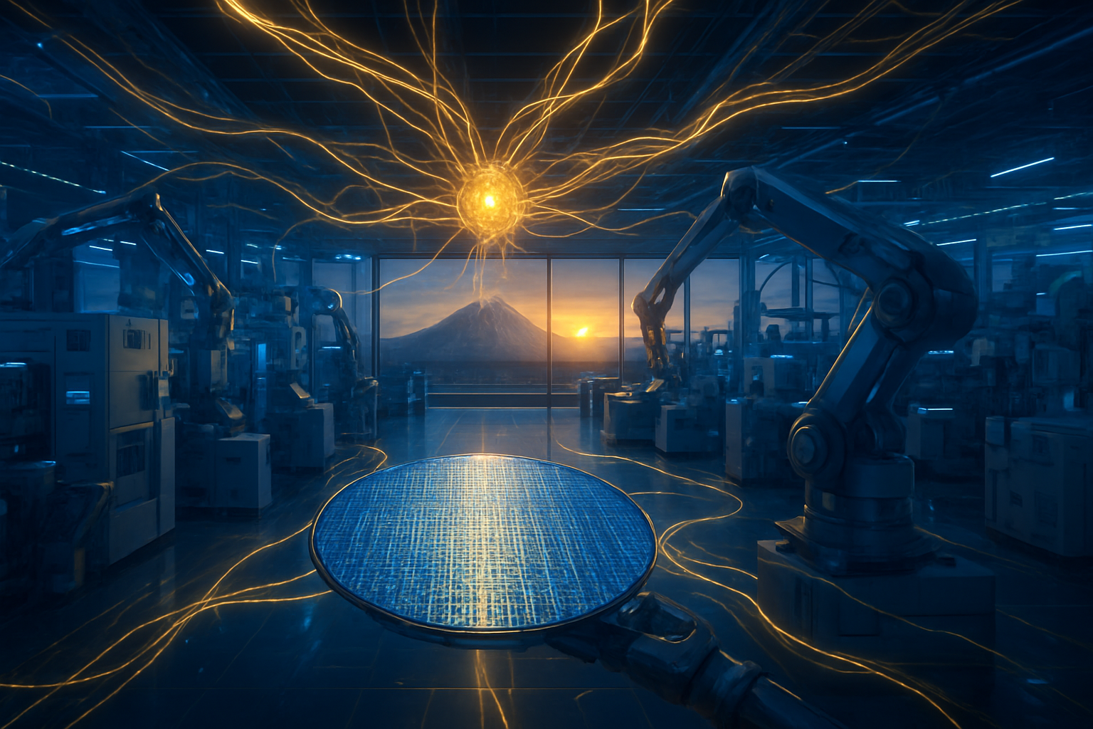
Tag: TSMC

  • Intel Challenges TSMC with Smartphone-Sized 10,000mm² Multi-Chiplet Processor Design

    Intel Challenges TSMC with Smartphone-Sized 10,000mm² Multi-Chiplet Processor Design

    In a move that signals a seismic shift in the semiconductor landscape, Intel (NASDAQ: INTC) has unveiled a groundbreaking conceptual multi-chiplet package with a massive 10,296 mm² silicon footprint. Roughly 12 times the size of today’s largest AI processors and comparable in dimensions to a modern smartphone, this "super-chip" represents the pinnacle of Intel’s "Systems Foundry" vision. By shattering the traditional lithography reticle limit, Intel is positioning itself to deliver unprecedented AI compute density, aiming to consolidate the power of an entire data center rack into a single, modular silicon entity.

    This announcement comes at a critical juncture for the industry, as the demand for Large Language Model (LLM) training and generative AI continues to outpace the physical limits of monolithic chip design. By integrating 16 high-performance compute elements with advanced memory and power delivery systems, Intel is not just manufacturing a processor; it is engineering a complete high-performance computing system on a substrate. The design serves as a direct challenge to the dominance of TSMC (NYSE: TSM), signaling that the race for AI supremacy will be won through advanced 2.5D and 3D packaging as much as through raw transistor scaling.

    Technical Breakdown: The 14A and 18A Synergy

    The "smartphone-sized" floorplan is a masterclass in heterogeneous integration, utilizing a mix of Intel’s most advanced process nodes. At the heart of the design are 16 large compute elements produced on the Intel 14A (1.4nm-class) process. These tiles leverage second-generation RibbonFET Gate-All-Around (GAA) transistors and PowerDirect—Intel’s sophisticated backside power delivery system—to achieve extreme logic density and performance-per-watt. By separating the power network from signal routing, Intel has effectively eliminated the "wiring bottleneck" that plagues traditional high-end silicon.

    Supporting these compute tiles are eight large base dies manufactured on the Intel 18A-PT node. Unlike the passive interposers used in many current designs, these are active silicon layers packed with massive amounts of embedded SRAM. This architecture, reminiscent of the "Clearwater Forest" design, allows for ultra-low-latency data movement between the compute engines and the memory subsystem. Surrounding this core are 24 HBM5 (High Bandwidth Memory 5) stacks, providing the multi-terabyte-per-second throughput necessary to feed the voracious appetite of the 14A logic array.

    To hold this massive 10,296 mm² assembly together, Intel utilizes a "3.5D" packaging approach. This includes Foveros Direct 3D, which enables vertical stacking with a sub-9µm copper-to-copper pitch, and EMIB-T (Embedded Multi-die Interconnect Bridge), which provides high-bandwidth horizontal connections between the base dies and HBM5 modules. This combination allows Intel to overcome the ~830 mm² reticle limit—the physical boundary of what a single lithography pass can print—by stitching multiple reticle-sized regions into a unified, coherent processor.

    Strategic Implications for the AI Ecosystem

    The unveiling of this design has immediate ramifications for tech giants and AI labs. Intel’s "Systems Foundry" approach is designed to attract hyperscalers like Microsoft (NASDAQ: MSFT) and Amazon (NASDAQ: AMZN), who are increasingly looking to design their own custom silicon. Microsoft has already confirmed its commitment to the Intel 18A process for its future Maia AI processors, and this new 10,000 mm² design provides a blueprint for how those chips could scale into the next decade.

    Perhaps the most surprising development is the warming relationship between Intel and NVIDIA (NASDAQ: NVDA). As NVIDIA seeks to diversify its supply chain and hedge against TSMC’s capacity constraints, it has reportedly explored Intel’s Foveros and EMIB packaging for its future Blackwell-successor architectures. The ability to "mix and match" compute dies from various nodes—such as pairing an NVIDIA GPU tile with Intel’s 18A base dies—gives Intel a unique strategic advantage. This flexibility could disrupt the current market positioning where TSMC’s CoWoS (Chip on Wafer on Substrate) is the only viable path for high-end AI hardware.

    The Broader AI Landscape and the 5,000W Frontier

    This development fits into a broader trend of "system-centric" silicon design. As the industry moves toward Artificial General Intelligence (AGI), the bottleneck has shifted from how many transistors can fit on a chip to how much power and data can be delivered to those transistors. Intel’s design is a "technological flex" that addresses this head-on, with future variants of the Foveros-B packaging rumored to support power delivery of up to 5,000W per module.

    However, such massive power requirements raise significant concerns regarding thermal management and infrastructure. Cooling a "smartphone-sized" chip that consumes as much power as five average households will require revolutionary liquid-cooling and immersion solutions. Comparisons are already being drawn to the Cerebras (Private) Wafer-Scale Engine; however, while Cerebras uses an entire monolithic wafer, Intel’s chiplet-based approach offers a more practical path to high yields and heterogeneous integration, allowing for more complex logic configurations than a single-wafer design typically permits.

    Future Horizons: From Concept to "Jaguar Shores"

    Looking ahead, this 10,296 mm² design is widely considered the precursor to Intel’s next-generation AI accelerator, codenamed "Jaguar Shores." While Intel’s immediate focus remains on the H1 2026 ramp of Clearwater Forest and the stabilization of the 18A node, the 14A roadmap points to a 2027 timeframe for volume production of these massive multi-chiplet systems.

    The potential applications for such a device are vast, ranging from real-time global climate modeling to the training of trillion-parameter models in a fraction of the current time. The primary challenge remains execution. Intel must prove it can achieve viable yields on the 14A node and that its EMIB-T interconnects can maintain signal integrity across such a massive physical distance. If successful, the "Jaguar Shores" era could redefine what is possible in the realm of edge-case AI and autonomous research.

    A New Chapter in Semiconductor History

    Intel’s unveiling of the 10,296 mm² multi-chiplet design marks a pivotal moment in the history of computing. It represents the transition from the era of the "Micro-Processor" to the era of the "System-Processor." By successfully integrating 16 compute elements and HBM5 into a single smartphone-sized footprint, Intel has laid down a gauntlet for TSMC and Samsung, proving that it still possesses the engineering prowess to lead the high-performance computing market.

    As we move into 2026, the industry will be watching closely to see if Intel can translate this conceptual brilliance into high-volume manufacturing. The strategic partnerships with NVIDIA and Microsoft suggest that the market is ready for a second major foundry player. If Intel can hit its 14A milestones, this "smartphone-sized" giant may very well become the foundation upon which the next generation of AI is built.


    This content is intended for informational purposes only and represents analysis of current AI developments.

    TokenRing AI delivers enterprise-grade solutions for multi-agent AI workflow orchestration, AI-powered development tools, and seamless remote collaboration platforms.
    For more information, visit https://www.tokenring.ai/.

  • TSMC Enters the 2nm Era: Volume Production Officially Begins at Fab 22

    TSMC Enters the 2nm Era: Volume Production Officially Begins at Fab 22

    KAOHSIUNG, Taiwan — In a landmark moment for the semiconductor industry, Taiwan Semiconductor Manufacturing Company (NYSE:TSM) has officially commenced volume production of its next-generation 2nm (N2) process technology. The rollout is centered at the newly operational Fab 22 in the Nanzih Science Park of Kaohsiung, marking the most significant architectural shift in chip manufacturing in over a decade. As of December 31, 2025, TSMC has successfully transitioned from the long-standing FinFET (Fin Field-Effect Transistor) structure to a sophisticated Gate-All-Around (GAA) nanosheet architecture, setting a new benchmark for the silicon that will power the next wave of artificial intelligence.

    The commencement of 2nm production arrives at a critical juncture for the global tech economy. With the demand for AI-specific compute power reaching unprecedented levels, the N2 node promises to provide the efficiency and density required to sustain the current pace of AI innovation. Initial reports from the Kaohsiung facility indicate that yield rates have already surpassed 65%, a remarkably high figure for a first-generation GAA node, signaling that TSMC is well-positioned to meet the massive order volumes expected from industry leaders in 2026.

    The Nanosheet Revolution: Inside the N2 Process

    The transition to the N2 node represents more than just a reduction in size; it is a fundamental redesign of how transistors function. For the past decade, the industry has relied on FinFET technology, where the gate sits on three sides of the channel. However, as transistors shrunk below 3nm, FinFETs began to struggle with current leakage and power efficiency. The new GAA nanosheet architecture at Fab 22 solves this by surrounding the channel on all four sides with the gate. This provides superior electrostatic control, drastically reducing power leakage and allowing for finer tuning of performance characteristics.

    Technically, the N2 node is a powerhouse. Compared to the previous N3E (enhanced 3nm) process, the 2nm technology is expected to deliver a 10-15% performance boost at the same power level, or a staggering 25-30% reduction in power consumption at the same speed. Furthermore, the N2 process introduces super-high-performance metal-insulator-metal (SHPMIM) capacitors, which double the capacitance density. This advancement significantly improves power stability, a crucial requirement for high-performance computing (HPC) and AI accelerators that operate under heavy, fluctuating workloads.

    Industry experts and researchers have reacted with cautious optimism. While the shift to GAA was long anticipated, the successful volume ramp-up at Fab 22 suggests that TSMC has overcome the complex lithography and materials science challenges that have historically delayed such transitions. "The move to nanosheets is the 'make-or-break' moment for sub-2nm scaling," noted one senior semiconductor analyst. "TSMC’s ability to hit volume production by the end of 2025 gives them a significant lead in providing the foundational hardware for the next decade of AI."

    A Strategic Leap for AMD and the AI Hardware Race

    The immediate beneficiary of this milestone is Advanced Micro Devices (NASDAQ:AMD), which has already confirmed its role as a lead customer for the N2 node. AMD plans to utilize the 2nm process for its upcoming Zen 6 "Venice" CPUs and the highly anticipated Instinct MI450 AI accelerators. By securing 2nm capacity, AMD aims to gain a competitive edge over its primary rival, NVIDIA (NASDAQ:NVDA). While NVIDIA’s upcoming "Rubin" architecture is expected to remain on a refined 3nm-class node, AMD’s shift to 2nm for its MI450 core dies could offer superior energy efficiency and compute density—critical metrics for the massive data centers operated by companies like OpenAI and Microsoft (NASDAQ:MSFT).

    The impact extends beyond AMD. Apple (NASDAQ:AAPL), traditionally TSMC's largest customer, is expected to transition its "Pro" series silicon to the N2 node for the 2026 iPhone and Mac refreshes. The strategic advantage of 2nm is clear: it allows device manufacturers to either extend battery life significantly or pack more neural processing units (NPUs) into the same thermal envelope. For the burgeoning market of AI PCs and AI-integrated smartphones, this efficiency is the "holy grail" that enables on-device LLMs (Large Language Models) to run without draining battery life in minutes.

    Meanwhile, the competition is intensifying. Intel (NASDAQ:INTC) is racing to catch up with its 18A process, which also utilizes a GAA-style architecture (RibbonFET), while Samsung (KRX:005930) has been producing GAA-based chips at 3nm with mixed success. TSMC’s successful volume production at Fab 22 reinforces its dominance, providing a stable, high-yield platform that major tech giants prefer for their flagship products. The "GIGAFAB" status of Fab 22 ensures that as demand for 2nm scales, TSMC will have the physical footprint to keep pace with the exponential growth of AI infrastructure.

    Redefining the AI Landscape and the Sustainability Challenge

    The broader significance of the 2nm era lies in its potential to address the "AI energy crisis." As AI models grow in complexity, the energy required to train and run them has become a primary concern for both tech companies and environmental regulators. The 25-30% power reduction offered by the N2 node is not just a technical spec; it is a necessary evolution to keep the AI industry sustainable. By allowing data centers to perform more operations per watt, TSMC is effectively providing a release valve for the mounting pressure on global energy grids.

    Furthermore, this milestone marks a continuation of Moore's Law, albeit through increasingly complex and expensive means. The transition to GAA at Fab 22 proves that silicon scaling still has room to run, even as we approach the physical limits of the atom. However, this progress comes with a "geopolitical premium." The concentration of 2nm production in Taiwan, particularly at the new Kaohsiung hub, underscores the world's continued reliance on a single geographic point for its most advanced technology. This has prompted ongoing discussions about supply chain resilience and the strategic importance of TSMC's expanding global footprint, including its future sites in Arizona and Japan.

    Comparatively, the jump to 2nm is being viewed as a more significant leap than the transition from 5nm to 3nm. While 3nm was an incremental improvement of the FinFET design, 2nm is a "clean sheet" approach. This architectural reset allows for a level of design flexibility—such as varying nanosheet widths—that will enable chip designers to create highly specialized silicon for specific AI tasks, ranging from ultra-low-power edge devices to massive, multi-die AI training clusters.

    The Road to 1nm: What Lies Ahead

    Looking toward the future, the N2 node is just the beginning of a multi-year roadmap. TSMC has already signaled that an enhanced version, N2P, will follow in late 2026, featuring backside power delivery—a technique that moves power lines to the rear of the wafer to reduce interference and further boost performance. Beyond that, the company is already laying the groundwork for the A16 (1.6nm) node, which is expected to integrate "Super Power Rail" technology and utilize High-NA EUV (Extreme Ultraviolet) lithography machines.

    In the near term, the industry will be watching the performance of the first Zen 6 and MI450 samples. If these chips deliver the 70% performance gains over current generations that some analysts predict, it could trigger a massive upgrade cycle across the enterprise and consumer sectors. The challenge for TSMC and its partners will be managing the sheer complexity of these designs. As features shrink, the risk of "silent data errors" and manufacturing defects increases, requiring even more advanced testing and packaging solutions like CoWoS (Chip-on-Wafer-on-Substrate).

    The next 12 to 18 months will be a period of intense validation. As Fab 22 ramps up to full capacity, the tech world will finally see if the promises of the 2nm era translate into a tangible acceleration of AI capabilities. If successful, the GAA transition will be remembered as the moment that gave AI the "silicon lungs" it needed to breathe and grow into its next phase of evolution.

    Conclusion: A New Chapter in Silicon History

    The official start of 2nm volume production at TSMC’s Fab 22 is a watershed moment. It represents the culmination of billions of dollars in R&D and years of engineering effort to move past the limitations of FinFET. By successfully launching the industry’s first high-volume GAA nanosheet process, TSMC has not only secured its market leadership but has also provided the essential hardware foundation for the next generation of AI-driven products.

    The key takeaways are clear: the AI industry now has a path to significantly higher efficiency and performance, AMD and Apple are poised to lead the charge in 2026, and the technical hurdles of GAA have been largely cleared. As we move into 2026, the focus will shift from "can it be built?" to "how fast can it be deployed?" The silicon coming out of Kaohsiung today will be the brains of the world's most advanced AI systems tomorrow.

    In the coming weeks, watch for further announcements regarding TSMC’s yield stability and potential additional lead customers joining the 2nm roster. The era of the nanosheet has begun, and the tech landscape will never be the same.


    This content is intended for informational purposes only and represents analysis of current AI developments.

    TokenRing AI delivers enterprise-grade solutions for multi-agent AI workflow orchestration, AI-powered development tools, and seamless remote collaboration platforms.
    For more information, visit https://www.tokenring.ai/.

  • The Silicon Fast Track: How the ‘Building Chips in America’ Act is Redrawing the Global AI Map

    The Silicon Fast Track: How the ‘Building Chips in America’ Act is Redrawing the Global AI Map

    As of late 2025, the landscape of American industrial policy has undergone a seismic shift, catalyzed by the full implementation of the "Building Chips in America" Act. Signed into law in late 2024, this legislation was designed as a critical "patch" for the original CHIPS and Science Act, addressing the bureaucratic bottlenecks that threatened to derail the most ambitious domestic manufacturing effort in decades. By exempting key semiconductor projects from the grueling multi-year environmental review process mandated by the National Environmental Policy Act (NEPA), the federal government has effectively hit the "fast-forward" button on the construction of the massive "fabs" that will power the next generation of artificial intelligence.

    The immediate significance of this legislative pivot cannot be overstated. In a year where AI demand has shifted from experimental large language models to massive-scale enterprise deployment, the physical infrastructure of silicon has become the ultimate strategic asset. The Act has allowed projects that were once mired in regulatory purgatory to break ground or accelerate their timelines, ensuring that the hardware necessary for AI—from H100 successors to custom silicon for hyperscalers—is increasingly "Made in America."

    Streamlining the Silicon Frontier

    The "Building Chips in America" Act (BCAA) specifically targets the National Environmental Policy Act of 1969, a foundational environmental law that requires federal agencies to assess the environmental effects of proposed actions. While intended to protect the ecosystem, NEPA reviews for complex industrial sites like semiconductor fabs typically take four to six years to complete. The BCAA introduced several critical "off-ramps" for these projects: any facility that commenced construction by December 31, 2024, was granted an automatic exemption; projects where federal grants account for less than 10% of the total cost are also exempt; and those receiving assistance solely through federal loans or loan guarantees bypass the review entirely.

    Technically, the Act also expanded "categorical exclusions" for the modernization of existing facilities, provided the expansion does not more than double the original footprint. This has allowed legacy fabs in states like Oregon and New York to upgrade their equipment for more advanced nodes without triggering a fresh environmental impact statement. For projects that still require some level of oversight, the Department of Commerce has been designated as the "lead agency," centralizing the process to prevent redundant evaluations by multiple federal bodies.

    Initial reactions from the AI research community and hardware industry have been overwhelmingly positive regarding the speed of execution. Industry experts note that the "speed-to-market" for a new fab is often the difference between a project being commercially viable or obsolete by the time it opens. By cutting the regulatory timeline by up to 60%, the U.S. has significantly narrowed the gap with manufacturing hubs in East Asia, where permitting processes are notoriously streamlined. However, the move has not been without controversy, as environmental groups have raised concerns over the long-term impact of "forever chemicals" (PFAS) used in chipmaking, which may now face less federal scrutiny.

    Divergent Paths: TSMC's Triumph and Intel's Patience

    The primary beneficiaries of this legislative acceleration are the titans of the industry: Taiwan Semiconductor Manufacturing Company (NYSE: TSM) and Intel Corporation (NASDAQ: INTC). For TSMC, the BCAA served as a tailwind for its Phoenix, Arizona, expansion. As of late 2025, TSMC’s Fab 21 (Phase 1) has successfully transitioned from trial production to high-volume manufacturing of 4nm and 5nm nodes. In a surprising turn for the industry, mid-2025 data revealed that TSMC’s Arizona yields were actually 4% higher than comparable facilities in Taiwan, a milestone that has validated the feasibility of high-end American manufacturing. TSMC Arizona even recorded its first-ever profit in the first half of 2025, a significant psychological win for the "onshoring" movement.

    Conversely, Intel’s "Ohio One" project in New Albany has faced a more complicated 2025. Despite the regulatory relief provided by the BCAA, Intel announced in July 2025 a strategic "slowing of construction" to align with market demand and corporate restructuring goals. While the first Ohio fab is now slated for completion in 2030, the BCAA has at least ensured that when Intel is ready to ramp up, it will not be held back by federal red tape. This has created a divergent market positioning: TSMC is currently the dominant domestic provider of leading-edge AI silicon, while Intel is positioning its Ohio and Oregon sites as the long-term backbone of a "system foundry" model for the 2030s.

    For AI startups and major labs like OpenAI and Anthropic, these domestic developments provide a critical strategic advantage. By having leading-edge manufacturing on U.S. soil, these companies are less vulnerable to the geopolitical volatility of the Taiwan Strait. The proximity of design and manufacturing also allows for tighter feedback loops in the creation of custom AI accelerators (ASICs), potentially disrupting the current market dominance of general-purpose GPUs.

    A National Security Imperative vs. Environmental Costs

    The "Building Chips in America" Act is a cornerstone of the U.S. government’s goal to produce 20% of the world’s leading-edge logic chips by 2030. In the broader AI landscape, this represents a return to "hard tech" industrialism. For decades, the U.S. focused on software and design while outsourcing the "dirty" work of manufacturing. The BCAA signals a realization that in the age of AI, the software layer is only as secure as the hardware it runs on. This shift mirrors previous milestones like the Apollo program or the interstate highway system, where national security and economic policy merged into a single infrastructure mandate.

    However, the wider significance also includes a growing tension between industrial progress and environmental justice. Organizations like the Sierra Club have argued that the BCAA "silences fenceline communities" by removing mandatory public comment periods. The semiconductor industry is water-intensive and utilizes hazardous chemicals; by bypassing NEPA, critics argue the government is prioritizing silicon over soil. This has led to a patchwork of state-level environmental regulations filling the void, with states like Arizona and Ohio implementing their own rigorous (though often faster) oversight mechanisms to appease local concerns.

    Comparatively, this era is being viewed as the "Silicon Renaissance." While the original CHIPS Act provided the capital, the BCAA provided the velocity. The 20% goal, which seemed like a pipe dream in 2022, now looks increasingly attainable, though experts warn that a "CHIPS 2.0" package may be needed by 2027 to subsidize the higher operational costs of U.S. labor compared to Asian counterparts.

    The Horizon: 2nm and the Automated Fab

    Looking ahead, the near-term focus will shift from "breaking ground" to "installing tools." In 2026, we expect to see the first 2nm "pathfinder" equipment arriving at TSMC’s Arizona Fab 3, which broke ground in April 2025. This will be the first time the world's most advanced semiconductor node is produced simultaneously in the U.S. and Taiwan. For AI, this means the next generation of models will likely be trained on domestic silicon from day one, rather than waiting for a delayed global rollout.

    The long-term challenge remains the workforce. While the BCAA solved the regulatory hurdle, the "talent hurdle" persists. Experts predict that by 2030, the U.S. semiconductor industry will face a shortage of nearly 70,000 technicians and engineers. Future developments will likely include massive federal investment in vocational training and "semiconductor academies," possibly integrated directly into the new fab clusters in Ohio and Arizona. We may also see the emergence of "AI-automated fabs," where robotics and machine learning are used to offset higher U.S. labor costs, further integrating AI into its own birth process.

    A New Era of Industrial Sovereignty

    The "Building Chips in America" Act of late 2024 has proven to be the essential lubricant for the machinery of the CHIPS Act. By late 2025, the results are visible in the rising skylines of Phoenix and New Albany. The key takeaways are clear: the U.S. has successfully decoupled its high-end chip supply from a purely offshore model, TSMC has proven that American yields can match or exceed global benchmarks, and the federal government has shown a rare willingness to sacrifice regulatory tradition for the sake of technological sovereignty.

    In the history of AI, the BCAA will likely be remembered as the moment the U.S. secured its "foundational layer." While the software breakthroughs of the early 2020s grabbed the headlines, the legislative and industrial maneuvers of 2024 and 2025 provided the physical reality that made those breakthroughs sustainable. As we move into 2026, the world will be watching to see if this "Silicon Fast Track" can maintain its momentum or if the environmental and labor challenges will eventually force a slowdown in the American chip-making machine.


    This content is intended for informational purposes only and represents analysis of current AI developments.

    TokenRing AI delivers enterprise-grade solutions for multi-agent AI workflow orchestration, AI-powered development tools, and seamless remote collaboration platforms.
    For more information, visit https://www.tokenring.ai/.

  • The Silicon Squeeze: Why Advanced Packaging is the New Gatekeeper of the AI Revolution in 2025

    The Silicon Squeeze: Why Advanced Packaging is the New Gatekeeper of the AI Revolution in 2025

    As of December 30, 2025, the narrative of the global AI race has shifted from a battle over transistor counts to a desperate scramble for "back-end" real estate. For the past decade, the semiconductor industry focused on the front-end—the complex lithography required to etch circuits onto silicon wafers. However, in the closing days of 2025, the industry has hit a physical wall. The primary bottleneck for the world’s most powerful AI chips is no longer the ability to print them, but the ability to package them. Advanced packaging technologies like TSMC’s CoWoS and Intel’s Foveros have become the most precious commodities in the tech world, dictating the pace of progress for every major AI lab from San Francisco to Beijing.

    The significance of this shift cannot be overstated. With lead times for flagship AI accelerators like NVIDIA’s Blackwell architecture stretching to 18 months, the "Silicon Squeeze" has turned advanced packaging into a strategic geopolitical asset. As demand for generative AI and massive language models continues to outpace supply, the ability to "stitch" together multiple silicon dies into a single high-performance module is the only way to bypass the physical limits of traditional chip manufacturing. In 2025, the "chiplet" revolution has officially arrived, and those who control the packaging lines now control the future of artificial intelligence.

    The Technical Wall: Reticle Limits and the Rise of CoWoS-L

    The technical crisis of 2025 stems from a physical constraint known as the "reticle limit." For years, semiconductor manufacturers like Taiwan Semiconductor Manufacturing Co. (NYSE: TSM) could simply make a single chip larger to increase its power. However, standard lithography tools can only expose an area of approximately 858 mm² at once. NVIDIA (NASDAQ: NVDA) reached this limit with its previous generations, but the demands of 2025-era AI require far more silicon than a single exposure can provide. To solve this, the industry has moved toward heterogeneous integration—combining multiple smaller "chiplets" onto a single substrate to act as one giant processor.

    TSMC has maintained its lead through CoWoS-L (Chip on Wafer on Substrate – Local Silicon Interconnect). Unlike previous iterations that used a massive, expensive silicon interposer, CoWoS-L utilizes tiny silicon bridges to link dies with massive bandwidth. This technology is the backbone of the NVIDIA Blackwell (B200) and the upcoming Rubin (R100) architectures. The Rubin chip, entering volume production as 2025 draws to a close, is a marvel of engineering that scales to a "4x reticle" design, effectively stitching together four standard-sized chips into a single super-processor. This complexity, however, comes at a cost: yield rates for these multi-die modules remain volatile, and a single defect in one of the 16 integrated HBM4 (High Bandwidth Memory) stacks can ruin a module worth tens of thousands of dollars.

    The High-Stakes Rivalry: Intel’s $5 Billion Diversification and AMD’s Acceleration

    The packaging bottleneck has forced a radical reshuffling of industry alliances. In one of the most significant strategic pivots of the year, NVIDIA reportedly invested $5 billion into Intel (NASDAQ: INTC) Foundry Services in late 2025. This move was designed to secure capacity for Intel’s Foveros 3D stacking and EMIB (Embedded Multi-die Interconnect Bridge) technologies, providing NVIDIA with a vital "Plan B" to reduce its total reliance on TSMC. Intel’s aggressive expansion of its packaging facilities in Malaysia and Oregon has positioned it as the only viable Western alternative for high-end AI assembly, a goal CEO Pat Gelsinger has pursued relentlessly to revitalize the company’s foundry business.

    Meanwhile, Advanced Micro Devices (NASDAQ: AMD) has accelerated its own roadmap to capitalize on the supply gaps. The AMD Instinct MI350 series, launched in mid-2025, utilizes a sophisticated 3D chiplet architecture that rivals NVIDIA’s Blackwell in memory density. To bypass the TSMC logjam, AMD has turned to "Outsourced Semiconductor Assembly and Test" (OSAT) giants like ASE Technology Holding (NYSE: ASX) and Amkor Technology (NASDAQ: AMKR). These firms are rapidly building out "CoWoS-like" capacity in Arizona and Taiwan, though they too are hampered by 12-month lead times for the specialized equipment required to handle the ultra-fine interconnects of 2025-grade silicon.

    The Wider Significance: Geopolitics and the End of Monolithic Computing

    The shift to advanced packaging represents the end of the "monolithic era" of computing. For fifty years, the industry followed Moore’s Law by shrinking transistors on a single piece of silicon. In 2025, that era is over. The future is modular, and the economic implications are profound. Because advanced packaging is so capital-intensive and requires such high precision, it has created a new "moat" that favors the largest incumbents. Hyperscalers like Meta (NASDAQ: META), Microsoft (NASDAQ: MSFT), and Amazon (NASDAQ: AMZN) are now pre-booking packaging capacity up to two years in advance, a practice that effectively crowds out smaller AI startups and academic researchers.

    This bottleneck also has a massive impact on the global supply chain's resilience. Most advanced packaging still occurs in East Asia, creating a single point of failure that keeps policymakers in Washington and Brussels awake at night. While the U.S. CHIPS Act has funded domestic fabrication plants, the "back-end" packaging remains the missing link. In late 2025, we are seeing the first real efforts to "reshore" this capability, with new facilities in the American Southwest beginning to come online. However, the transition is slow; the expertise required for 2.5D and 3D integration is highly specialized, and the labor market for packaging engineers is currently the tightest in the tech sector.

    The Next Frontier: Glass Substrates and Panel-Level Packaging

    Looking toward 2026 and 2027, the industry is already searching for the next breakthrough to break the current bottleneck. The most promising development is the transition to glass substrates. Traditional organic substrates are prone to warping and heat-related issues as chips get larger and hotter. Glass offers superior flatness and thermal stability, allowing for even denser interconnects. Intel is currently leading the charge in glass substrate research, with plans to integrate the technology into its 2026 product lines. If successful, glass could allow for "system-in-package" designs that are significantly larger than anything possible today.

    Furthermore, the industry is eyeing Panel-Level Packaging (PLP). Currently, chips are packaged on circular 300mm wafers, which results in significant wasted space at the edges. PLP uses large rectangular panels—similar to those used in the display industry—to process hundreds of chips at once. This could potentially increase throughput by 3x to 4x, finally easing the supply constraints that have defined 2025. However, the transition to PLP requires an entirely new ecosystem of equipment and materials, meaning it is unlikely to provide relief for the current Blackwell and MI350 backlogs until at least late 2026.

    Summary of the 2025 Silicon Landscape

    As 2025 draws to a close, the semiconductor industry has successfully navigated the challenges of sub-3nm fabrication, only to find itself trapped by the physical limits of how those chips are put together. The "Silicon Squeeze" has made advanced packaging the ultimate arbiter of AI power. NVIDIA’s 18-month lead times and the strategic move toward Intel’s packaging lines underscore a new reality: in the AI era, it’s not just about what you can build on the silicon, but how much silicon you can link together.

    The coming months will be defined by how quickly TSMC, Intel, and Samsung (KRX: 005930) can scale their 3D stacking capacities. For investors and tech leaders, the metrics to watch are no longer just wafer starts, but "packaging out-turns" and "interposer yields." As we head into 2026, the companies that master the art of the chiplet will be the ones that define the next plateau of artificial intelligence. The revolution is no longer just in the code—it’s in the package.


    This content is intended for informational purposes only and represents analysis of current AI developments.

    TokenRing AI delivers enterprise-grade solutions for multi-agent AI workflow orchestration, AI-powered development tools, and seamless remote collaboration platforms.
    For more information, visit https://www.tokenring.ai/.

  • Intel’s $380 Million Gamble: High-NA EUV Deployment at Fab 52 Marks New Era in 1.4nm Race

    Intel’s $380 Million Gamble: High-NA EUV Deployment at Fab 52 Marks New Era in 1.4nm Race

    As of late December 2025, the semiconductor industry has reached a pivotal turning point with Intel Corporation (NASDAQ: INTC) officially operationalizing the world’s first commercial-grade High-Numerical Aperture (High-NA) Extreme Ultraviolet (EUV) lithography systems. At the heart of this technological leap is Intel’s Fab 52 in Chandler, Arizona, where the deployment of ASML (NASDAQ: ASML) Twinscan EXE:5200B machines marks a high-stakes bet on reclaiming the crown of process leadership. This move signals the beginning of the "Angstrom Era," as Intel prepares to transition its 1.4nm (14A) node into risk production, a feat that could redefine the competitive hierarchy of the global chip market.

    The immediate significance of this deployment cannot be overstated. By successfully integrating these $380 million machines into its high-volume manufacturing (HVM) workflow, Intel is attempting to leapfrog its primary rival, Taiwan Semiconductor Manufacturing Company (NYSE: TSM), which has opted for a more conservative roadmap. This strategic divergence comes at a critical time when the demand for ultra-efficient AI accelerators and high-performance computing (HPC) silicon is at an all-time high, making the precision and density offered by High-NA EUV the new "gold standard" for the next generation of artificial intelligence.

    The ASML Twinscan EXE:5200B represents a massive technical evolution over the standard "Low-NA" EUV tools that have powered the industry for the last decade. While standard EUV systems utilize a numerical aperture of 0.33, the High-NA variant increases this to 0.55. This improvement allows for a resolution jump from 13.5nm down to 8nm, enabling the printing of features that are nearly twice as small. For Intel, the primary advantage is the reduction of "multi-patterning." In previous nodes, complex layers required multiple passes through a scanner to achieve the necessary density, a process that is both time-consuming and prone to defects. The EXE:5200B allows for "single-patterning" on critical layers, potentially reducing the number of process steps from 40 down to fewer than 10 for certain segments of the chip.

    Technical specifications for the EXE:5200B are staggering. The machine stands two stories tall and weighs as much as two Airbus A320s. In terms of productivity, the 5200B model has achieved a throughput of 175 to 200 wafers per hour, a significant increase over the 125 wafers per hour managed by the earlier EXE:5000 research modules. This productivity gain is essential for making the $380 million-per-unit investment economically viable in a high-volume environment like Fab 52. Furthermore, the system boasts a 0.7nm overlay accuracy, ensuring that the billions of transistors on a 1.4nm chip are aligned with atomic-level precision.

    The reaction from the research community has been a mix of awe and cautious optimism. Experts note that while the hardware is revolutionary, the ecosystem—including photoresists, masks, and metrology tools—must catch up to the 0.55 NA standard. Intel’s early adoption is seen as a "trial by fire" that will mature the entire supply chain. Industry analysts have praised Intel’s engineering teams at the D1X facility in Oregon for the rapid validation of the 5200B, which allowed the Arizona deployment to happen months ahead of the original 2026 schedule.

    Intel’s "de-risking" strategy is a bold departure from the industry’s typical "wait-and-see" approach. By acting as the lead customer for High-NA EUV, Intel is absorbing the early technical hurdles and high costs associated with the new technology. The strategic advantage here is twofold: first, Intel gains a 2-3 year head start in mastering the High-NA ecosystem; second, it has designed its 14A node to be "design-rule compatible" with standard EUV. This means if the High-NA yields are initially lower than expected, Intel can fall back on traditional multi-patterning without requiring its customers to redesign their chips. This safety net is a key component of CEO Pat Gelsinger’s plan to restore investor confidence.

    For TSMC, the decision to delay High-NA adoption until its A14 or even A10 nodes (likely 2028 or later) is rooted in economic pragmatism. TSMC argues that standard EUV, combined with advanced multi-patterning and "Hyper-NA" techniques, remains more cost-effective for its current customer base, which includes Apple (NASDAQ: AAPL) and Nvidia (NASDAQ: NVDA). However, this creates a window of opportunity for Intel Foundry. If Intel can prove that High-NA leads to superior power-performance-area (PPA) metrics for AI chips, it may lure high-profile "anchor" customers away from TSMC’s more mature, yet technically older, processes.

    The ripple effects will also be felt by AI startups and fabless giants. Companies designing the next generation of Large Language Model (LLM) trainers require maximum transistor density to fit more HBM (High Bandwidth Memory) and compute cores on a single die. Intel’s 14A node, powered by High-NA, promises a 2.9x increase in transistor density over current 3nm processes. This could make Intel the preferred foundry for specialized AI silicon, disrupting the current near-monopoly held by TSMC in the high-end accelerator market.

    The deployment at Fab 52 takes place against a backdrop of intensifying geopolitical competition. Just as Intel reached its High-NA milestone, reports surfaced from Shenzhen, China, regarding a domestic EUV prototype breakthrough. A Chinese research consortium has reportedly validated a working EUV light source using Laser-Induced Discharge Plasma (LDP) technology. While this prototype is currently less efficient than ASML’s systems and years away from high-volume manufacturing, it signals that China is successfully navigating around Western export controls to build a "parallel supply chain."

    This development underscores the fragility of the "Silicon Shield" and the urgency of Intel’s mission. The global AI landscape is increasingly tied to the ability to manufacture at the leading edge. If China can eventually bridge the EUV gap, the technological advantage currently held by the U.S. and its allies could erode. Intel’s aggressive push into High-NA is not just a corporate strategy; it is a critical component of the U.S. government’s goal to secure domestic semiconductor manufacturing through the CHIPS Act.

    Comparatively, this milestone is being likened to the transition from 193nm immersion lithography to EUV in the late 2010s. That transition saw several players, including GlobalFoundries, drop out of the leading-edge race due to the immense costs. The High-NA transition appears to be having a similar effect, narrowing the field of "Angstrom-era" manufacturers to a tiny elite. The stakes are higher than ever, as the winner of this race will essentially dictate the hardware limits of artificial intelligence for the next decade.

    Looking ahead, the next 12 to 24 months will be focused on yield optimization. While the machines are now in place at Fab 52, the challenge lies in reaching "golden" yield levels that make 1.4nm chips commercially profitable. Intel expects its 14A-E (an enhanced version of the 14A node) to begin development shortly after the initial 14A rollout, further refining the use of High-NA for even more complex architectures. Potential applications on the horizon include "monolithic 3D" transistors and advanced backside power delivery, which will be integrated with High-NA patterning.

    Experts predict that the industry will eventually see a "convergence" where TSMC and Samsung (OTC: SSNLF) are forced to adopt High-NA by 2027 to remain competitive. The primary challenge that remains is the "reticle limit"—High-NA machines have a smaller field size, meaning chip designers must use "stitching" to create large AI chips. Mastering this stitching process will be the next major hurdle for Intel’s engineers. If successful, we could see the first 1.4nm AI accelerators hitting the market by late 2027, offering performance leaps that were previously thought to be a decade away.

    Intel’s successful deployment of the ASML Twinscan EXE:5200B at Fab 52 is a landmark achievement in the history of semiconductor manufacturing. It represents a $380 million-per-unit gamble that Intel can out-innovate its rivals by embracing complexity rather than avoiding it. The key takeaways from this development are Intel’s early lead in the 1.4nm race, the stark strategic divide between Intel and TSMC, and the emerging domestic threat from China’s lithography breakthroughs.

    As we move into 2026, the industry will be watching Intel’s yield reports with bated breath. The long-term impact of this deployment could be the restoration of the "Tick-Tock" model of innovation that once made Intel the undisputed leader of the tech world. For now, the "Angstrom Era" has officially arrived in Arizona, and the race to define the future of AI hardware is more intense than ever.


    This content is intended for informational purposes only and represents analysis of current AI developments.

    TokenRing AI delivers enterprise-grade solutions for multi-agent AI workflow orchestration, AI-powered development tools, and seamless remote collaboration platforms.
    For more information, visit https://www.tokenring.ai/.

  • The Sub-2nm Supremacy: Intel 18A Hits Volume Production as TSMC N2 Ramps for 2026

    The Sub-2nm Supremacy: Intel 18A Hits Volume Production as TSMC N2 Ramps for 2026

    As of late December 2025, the semiconductor industry has reached a historic inflection point that many analysts once thought impossible. Intel (NASDAQ:INTC) has officially successfully executed its "five nodes in four years" roadmap, culminating in the mid-2025 volume production of its 18A (1.8nm) process node. This achievement has effectively allowed the American chipmaker to leapfrog the industry’s traditional leader, Taiwan Semiconductor Manufacturing Company (NYSE:TSM), in the race to deploy the next generation of transistor architecture. With Intel’s "Panther Lake" processors already shipping to hardware partners for a January 2026 retail launch, the battle for silicon supremacy has moved from the laboratory to the high-volume factory floor.

    The significance of this moment cannot be overstated. For the first time in nearly a decade, the "process lead"—the metric by which the world’s most advanced chips are judged—is no longer a foregone conclusion in favor of TSMC. While TSMC has begun series production of its own N2 (2nm) node in late 2025, Intel’s early aggressive push with 18A has created a competitive vacuum. This shift is driving a massive realignment in the high-performance computing and AI sectors, as tech giants weigh the technical advantages of Intel’s new architecture against the legendary reliability and scale of the Taiwanese foundry.

    Technical Frontiers: RibbonFET and the PowerVia Advantage

    The transition to the 2nm class represents the most radical architectural change in semiconductors since the introduction of FinFET over a decade ago. Both Intel and TSMC have moved to Gate-All-Around (GAA) transistors—which Intel calls RibbonFET and TSMC calls Nanosheet GAA—to overcome the physical limitations of current designs. However, the technical differentiator that has put Intel in the spotlight is "PowerVia," the company's proprietary implementation of Backside Power Delivery (BSPDN). By moving power routing to the back of the wafer, Intel has decoupled power and signal wires, drastically reducing electrical interference and "voltage droop." This allows 18A chips to achieve higher clock speeds at lower voltages, a critical requirement for the energy-hungry AI workloads of 2026.

    In contrast, TSMC’s initial N2 node, while utilizing a highly refined Nanosheet GAA structure, has opted for a more conservative approach by maintaining traditional frontside power delivery. While this strategy has allowed TSMC to maintain slightly higher initial yields—reported at approximately 65–70% compared to Intel’s 55–65%—it leaves a performance gap that Intel is eager to exploit. TSMC’s version of backside power, the "Super Power Rail," is not scheduled to debut until the N2P and A16 (1.6nm) nodes arrive late in 2026 and throughout 2027. This technical window has given Intel a temporary but potent "performance-per-watt" lead that is reflected in the early benchmarks of its Panther Lake and Clearwater Forest architectures.

    Initial reactions from the semiconductor research community have been cautiously optimistic. Experts note that while Intel’s 18A density (roughly 238 million transistors per square millimeter) still trails TSMC’s N2 density (over 310 MTr/mm²), the efficiency gains from PowerVia may matter more for real-world AI performance than raw density alone. The industry is closely watching the "Panther Lake" (Core Ultra Series 3) launch, as it will be the first high-volume consumer product to prove whether Intel can maintain these technical gains without the manufacturing "stumbles" that plagued its 10nm and 7nm efforts years ago.

    The Foundry War: Client Loyalty and Strategic Shifts

    The business implications of this race are reshaping the landscape for AI companies and tech giants. Intel Foundry has already secured high-profile commitments from Microsoft (NASDAQ:MSFT) for its Maia 2 AI accelerators and Amazon (NASDAQ:AMZN) for custom Xeon 6 fabric silicon. These partnerships are a massive vote of confidence in Intel’s 18A node and signal a desire among US-based hyperscalers to diversify their supply chains away from a single-source reliance on Taiwan. For Intel, these "anchor" customers provide the volume necessary to refine 18A yields and fund the even more ambitious 14A node slated for 2027.

    Meanwhile, TSMC remains the dominant force by sheer volume and ecosystem maturity. Apple (NASDAQ:AAPL) has reportedly secured nearly 50% of TSMC’s initial N2 capacity for its upcoming A20 and M5 chips, ensuring that the next generation of iPhones and Macs remains at the bleeding edge. Similarly, Nvidia (NASDAQ:NVDA) is sticking with TSMC for its "Rubin" GPU successor, citing the foundry’s superior CoWoS packaging capabilities as a primary reason. However, the fact that Nvidia has reportedly kept a "placeholder" for testing Intel’s 18A yields suggests that even the AI kingpin is keeping its options open should Intel’s performance lead prove durable through 2026.

    This competition is disrupting the "wait-and-see" approach previously taken by many fabless startups. With Intel 18A offering a faster path to backside power delivery, some AI hardware startups are pivoting their designs to Intel’s PDKs (Process Design Kits) to gain a first-mover advantage in efficiency. The market positioning is clear: Intel is marketing itself as the "performance leader" for those who need the latest architectural breakthroughs now, while TSMC positions itself as the "reliable scale leader" for the world’s largest consumer electronics brands.

    Geopolitics and the End of the FinFET Era

    The broader significance of the 2nm race extends far beyond chip benchmarks; it is a central pillar of global technological sovereignty. Intel’s success with 18A is a major win for the U.S. CHIPS Act, as the node is being manufactured at scale in Fab 52 in Arizona. This represents a tangible shift in the geographic concentration of advanced logic manufacturing. As the world moves into the post-FinFET era, the ability to manufacture GAA transistors at scale has become the new baseline for being a "tier-one" tech superpower.

    This milestone also echoes previous industry shifts, such as the move from planar transistors to FinFET in 2011. Just as that transition allowed for the smartphone revolution, the move to 2nm and 1.8nm is expected to fuel the next decade of "Edge AI." By providing the thermal headroom needed to run large language models (LLMs) locally on laptops and mobile devices, these new nodes are the silent engines behind the AI software boom. The potential concern remains the sheer cost of these chips; as wafer prices for 2nm are expected to exceed $30,000, the "digital divide" between companies that can afford the latest silicon and those that cannot may widen.

    Future Outlook: The Road to 14A and A16

    Looking ahead to 2026, the industry will focus on the ramp-up of consumer availability. While Intel’s Panther Lake will dominate the conversation in early 2026, the second half of the year will see the debut of TSMC’s N2 in the iPhone 18, likely reclaiming the crown for mobile efficiency. Furthermore, the arrival of High-NA EUV (Extreme Ultraviolet) lithography machines from ASML (NASDAQ:ASML) will become the next battleground. Intel has already taken delivery of the first High-NA units to prepare for its 14A node, while TSMC has indicated it may wait until 2026 or 2027 to integrate the expensive new tools into its A16 process.

    Experts predict that the "lead" will likely oscillate between the two giants every 12 to 18 months. The next major hurdle will be the integration of "optical interconnects" and even more advanced 3D packaging, as the industry realizes that the transistor itself is no longer the only bottleneck. The success of Intel’s Clearwater Forest in mid-2026 will be the ultimate test of whether 18A can handle the grueling demands of the data center at scale, potentially paving the way for a permanent "dual-foundry" world where Intel and TSMC share the top spot.

    A New Era of Silicon Competition

    The 2nm manufacturing race of 2025-2026 marks the end of Intel’s period of "catch-up" and the beginning of a genuine two-way fight for the future of computing. By hitting volume production with 18A in mid-2025 and beating TSMC to the implementation of backside power delivery, Intel has proven that its turnaround strategy under Pat Gelsinger was more than just corporate rhetoric. However, TSMC’s massive capacity and deep-rooted relationships with Apple and Nvidia mean that the Taiwanese giant is far from losing its throne.

    As we move into early 2026, the key takeaways are clear: the era of FinFET is over, "PowerVia" is the new technical gold standard, and the geographic map of chip manufacturing is successfully diversifying. For consumers, this means more powerful "AI PCs" and smartphones are just weeks away from store shelves. For the industry, it means the most competitive and innovative period in semiconductor history has only just begun. Watch for the CES 2026 announcements in January, as they will provide the first retail evidence of who truly won the 2nm punch.


    This content is intended for informational purposes only and represents analysis of current AI developments.

    TokenRing AI delivers enterprise-grade solutions for multi-agent AI workflow orchestration, AI-powered development tools, and seamless remote collaboration platforms.
    For more information, visit https://www.tokenring.ai/.

  • The Backside Revolution: How PowerVia Propels Intel into the Lead of the AI Silicon Race

    The Backside Revolution: How PowerVia Propels Intel into the Lead of the AI Silicon Race

    As the calendar turns to late 2025, the semiconductor industry is witnessing its most profound architectural shift in over a decade. The arrival of Backside Power Delivery (BSPD), spearheaded by Intel Corporation (NASDAQ: INTC) and its proprietary PowerVia technology, has fundamentally altered the physics of chip design. By physically separating power delivery from signal routing, Intel has solved a decade-long "traffic jam" on the silicon wafer, providing a critical performance boost just as the demand for generative AI reaches its zenith.

    This breakthrough is not merely an incremental improvement; it is a total reimagining of how electricity reaches the billions of transistors that power modern AI models. While traditional chips struggle with electrical interference and "voltage drop" as they shrink, PowerVia allows for more efficient power distribution, higher clock speeds, and significantly denser logic. For Intel, this represents a pivotal moment in its "five nodes in four years" strategy, potentially reclaiming the manufacturing crown from long-time rival Taiwan Semiconductor Manufacturing Company (NYSE: TSM).

    Unclogging the Silicon Arteries: The PowerVia Advantage

    For nearly fifty years, chips have been built like a layer cake, with transistors at the bottom and all the wiring—both for data signals and power—layered on top. As transistors shrank to the "Angstrom" scale, these wires became so crowded that they began to interfere with one another. Power lines, which are relatively bulky, would block the path of delicate signal wires, leading to a phenomenon known as "crosstalk" and causing significant voltage drops (IR drop) as electricity struggled to navigate the maze. Intel’s PowerVia solves this by moving the entire power delivery network to the "backside" of the silicon wafer, leaving the "front side" exclusively for data signals.

    Technically, PowerVia achieves this through the use of nano-Through Silicon Vias (nTSVs). These are microscopic vertical tunnels that pass directly through the silicon substrate to connect the backside power layers to the transistors. This approach eliminates the need for power to travel through 10 to 20 layers of metal on the front side. By shortening the path to the transistor, Intel has successfully reduced IR drop by nearly 30%, allowing transistors to switch faster and more reliably. Initial data from Intel’s 18A node, currently in high-volume manufacturing, shows frequency gains of up to 6% at the same power level compared to traditional front-side designs.

    Beyond speed, the removal of power lines from the front side has unlocked a massive amount of "real estate" for logic. Chip designers can now pack transistors much closer together, achieving density improvements of up to 30%. This is a game-changer for AI accelerators, which require massive amounts of logic and memory to process large language models. The industry response has been one of cautious optimism followed by rapid adoption, as experts recognize that BSPD is no longer a luxury, but a necessity for the next generation of high-performance computing.

    A Two-Year Head Start: Intel 18A vs. TSMC A16

    The competitive landscape of late 2025 is defined by a rare "first-mover" advantage for Intel. While Intel’s 18A node is already powering the latest "Panther Lake" consumer chips and "Clearwater Forest" server processors, TSMC is still in the preparation phase for its own BSPD implementation. TSMC has opted to skip a basic backside delivery on its 2nm node, choosing instead to debut an even more advanced version, called Super PowerRail, on its A16 (1.6nm) process. However, A16 is not expected to reach high-volume production until the second half of 2026, giving Intel a roughly 1.5 to 2-year lead in the commercial application of this technology.

    This lead has already begun to shift the strategic positioning of major AI chip designers. Companies that have traditionally relied solely on TSMC, such as NVIDIA Corporation (NASDAQ: NVDA) and Apple Inc. (NASDAQ: AAPL), are now closely monitoring Intel's foundry yields. Intel’s 18A yields are currently reported to be stabilizing between 60% and 70%, a healthy figure for a node of this complexity. The pressure is now on TSMC to prove that its Super PowerRail—which connects power directly to the transistor’s source and drain rather than using Intel's nTSV method—will offer superior efficiency that justifies the wait.

    For the market, this creates a fascinating dynamic. Intel is using its manufacturing lead to lure high-profile foundry customers who are desperate for the power efficiency gains that BSPD provides. Microsoft Corporation (NASDAQ: MSFT) and Amazon.com, Inc. (NASDAQ: AMZN) have already signed on to use Intel’s advanced nodes for their custom AI silicon, such as the Maia 2 and Trainium 2 chips. This disruption to the existing foundry hierarchy could lead to a more diversified supply chain, reducing the industry's heavy reliance on a single geographic region for the world's most advanced chips.

    Powering the AI Infrastructure: Efficiency at Scale

    The wider significance of Backside Power Delivery cannot be overstated in the context of the global AI energy crisis. As data centers consume an ever-increasing share of the world’s electricity, the 15-20% performance-per-watt improvement offered by PowerVia is a critical sustainability tool. For hyperscale cloud providers, a 20% reduction in power consumption translates to hundreds of millions of dollars saved in cooling costs and electricity bills. BSPD is effectively "free performance" that helps mitigate the thermal throttling issues that have plagued high-wattage AI chips like NVIDIA's Blackwell series.

    Furthermore, BSPD enables a new era of "computational density." By clearing the front-side metal layers, engineers can more easily integrate High Bandwidth Memory (HBM) and implement complex chiplet architectures. This allows for larger logic dies on the same interposer, as the power delivery no longer clutters the high-speed interconnects required for chip-to-chip communication. This fits into the broader trend of "system-level" scaling, where the entire package, rather than just the individual transistor, is optimized for AI workloads.

    However, the transition to BSPD is not without its concerns. The manufacturing process is significantly more complex, requiring advanced wafer bonding and thinning techniques that increase the risk of defects. There are also long-term reliability questions regarding the thermal management of the backside power layers, which are now physically closer to the silicon substrate. Despite these challenges, the consensus among AI researchers is that the benefits far outweigh the risks, marking this as a milestone comparable to the introduction of FinFET transistors in the early 2010s.

    The Road to Sub-1nm: What Lies Ahead

    Looking toward 2026 and beyond, the industry is already eyeing the next evolution of power delivery. While Intel’s PowerVia and TSMC’s Super PowerRail are the current gold standard, research is already underway for "direct-to-gate" power delivery, which could further reduce resistance. We expect to see Intel refine its 18A process into "14A" by 2027, potentially introducing even more aggressive backside routing. Meanwhile, TSMC’s A16 will likely be the foundation for the first sub-1nm chips, where BSPD will be an absolute requirement for the transistors to function at all.

    The potential applications for this technology extend beyond the data center. As AI becomes more prevalent in "edge" devices, the power savings of BSPD will enable more sophisticated on-device AI for smartphones and wearable tech without sacrificing battery life. Experts predict that by 2028, every flagship processor in the world—from laptops to autonomous vehicles—will utilize some form of backside power delivery. The challenge for the next three years will be scaling these complex manufacturing processes to meet the insatiable global demand for silicon.

    A New Era of Silicon Sovereignty

    In summary, Backside Power Delivery represents a total architectural pivot that has arrived just in time to sustain the AI revolution. Intel’s PowerVia has provided the company with a much-needed technical edge, proving that its aggressive manufacturing roadmap was more than just marketing rhetoric. By being the first to market with 18A, Intel has forced the rest of the industry to accelerate their timelines, ultimately benefiting the entire ecosystem with more efficient and powerful hardware.

    As we look ahead to the coming months, the focus will shift from technical "proofs of concept" to high-volume execution. Watch for Intel's quarterly earnings reports and foundry updates to see if they can maintain their yield targets, and keep a close eye on TSMC’s A16 risk production milestones in early 2026. This is a marathon, not a sprint, but for the first time in a decade, the lead runner has changed, and the stakes for the future of AI have never been higher.


    This content is intended for informational purposes only and represents analysis of current AI developments.

    TokenRing AI delivers enterprise-grade solutions for multi-agent AI workflow orchestration, AI-powered development tools, and seamless remote collaboration platforms.
    For more information, visit https://www.tokenring.ai/.

  • Sustainability in the Fab: The Race for Net-Zero Water and Energy

    Sustainability in the Fab: The Race for Net-Zero Water and Energy

    As the artificial intelligence "supercycle" continues to accelerate, driving global chip sales to a record $72.7 billion in October 2025, the semiconductor industry is facing an unprecedented resource crisis. The transition to 2nm and 1.4nm manufacturing nodes has proven to be a double-edged sword: while these chips power the next generation of generative AI, their production requires up to 2.3 times more water and 3.5 times more electricity than previous generations. In response, the world’s leading foundries have transformed their operations, turning the "mega-fab" into a laboratory for radical sustainability and "Net-Zero" resource management.

    This shift has moved beyond corporate social responsibility into the realm of operational necessity. In late 2025, water scarcity in hubs like Arizona and Taiwan has made "Net-Positive" water status—where a company returns more water to the ecosystem than it withdraws—the new gold standard for the industry. From Micron’s billion-dollar conservation funds to TSMC’s pioneering reclaimed water plants, the race to build the first truly circular semiconductor ecosystem is officially on, powered by the very AI these facilities were built to produce.

    The Technical Frontiers of Ultrapure Water and Zero Liquid Discharge

    At the heart of the sustainability push is the management of Ultrapure Water (UPW), a substance thousands of times cleaner than pharmaceutical-grade water. In the 2nm era, even a "killer particle" as small as 10nm can ruin a wafer, making the purification process more intensive than ever. To combat the waste associated with this purity, companies like Micron Technology (NASDAQ: MU) have committed to a $1 billion sustainability initiative. As of late 2025, Micron has already deployed over $406 million of this fund, achieving a 66% global water conservation rate. Their planned $100 billion mega-fab in Clay, New York, is currently implementing a "Green CHIPS" framework designed to achieve near-100% water conservation through massive internal recycling loops.

    Taiwan Semiconductor Manufacturing Company (NYSE: TSM), or TSMC, has taken a different but equally ambitious path with its industrial-scale reclaimed water plants. In Taiwan’s Southern Taiwan Science Park, TSMC’s facilities reached a milestone in 2025, supplying nearly 67,000 metric tons of recycled water daily. Meanwhile, at its Phoenix, Arizona campus, TSMC broke ground in August 2025 on a new 15-acre Industrial Reclamation Water Plant (IRWP). Once fully operational, this facility is designed to recycle 90% of the fab's industrial wastewater, reducing the daily demand of a single fab from 4.75 million gallons to under 1.2 million gallons—a critical achievement in the water-stressed American Southwest.

    Technologically, these "Net-Zero" systems rely on a complex hierarchy of purification. Modern fabs in 2025 utilize segmented waste streams, separating chemical rinses from hydrofluoric acid waste to treat them individually. Advanced techniques such as Pulse-Flow Reverse Osmosis (PFRO) and Electrodeionization (EDI) are now standard, allowing for 98% water recovery. Furthermore, the introduction of 3D-printed spacers in membrane filtration—a technology backed by Micron—has significantly reduced the energy required to push water through these microscopic filters, addressing the energy-water nexus head-on.

    Competitive Advantages and the Rise of 'Green' Silicon

    The push for sustainability is reshaping the competitive landscape for chipmakers like Intel (NASDAQ: INTC) and Samsung Electronics (KRX: 005930). Intel’s Q4 2025 update confirmed that its 18A (1.8nm) process node is not just a performance leader but a sustainability one, delivering a 40% reduction in power consumption compared to older nodes. By simplifying the processing flow by 44% through advanced EUV lithography, Intel has reduced the total material intensity of its most advanced chips. This "green silicon" approach provides a strategic advantage as major customers like Microsoft (NASDAQ: MSFT) and NVIDIA (NASDAQ: NVDA) now demand verified "carbon and water receipts" for every wafer to meet their own 2030 net-zero goals.

    Samsung has countered with its own massive milestones, announcing in October 2025 that it achieved the UL Solutions "Zero Waste to Landfill" Platinum designation across all its global manufacturing sites. In South Korea, Samsung’s collaboration with the Ministry of Environment now supplies 120,000 tonnes of reclaimed water per day to its Giheung and Hwaseong fabs. For these giants, sustainability is no longer just about compliance; it is a market positioning tool. Foundries that can guarantee production continuity in water-stressed regions while lowering the carbon footprint of the end product are winning the lion's share of long-term supply contracts from sustainability-conscious tech titans.

    AI as the Architect of the Sustainable Fab

    Perhaps the most poetic development of 2025 is the use of AI to optimize the very factories that create it. "Agentic AI" ecosystems, such as those launched by Schneider Electric (EPA: SU) in mid-2025, now act as autonomous stewards of fab resources. these AI agents monitor thousands of sensors in real-time, making independent adjustments to chiller settings, HVAC airflow, and ultrapure water flow rates. This has led to an average 20% improvement in operational energy efficiency across modern mega-fabs.

    Digital Twin technology has also become a standard requirement for new construction. Companies like Applied Materials (NASDAQ: AMAT) are utilizing their EPIC platform to create high-fidelity virtual replicas of the manufacturing process. By simulating gas usage and chemical reactions before a single wafer is processed, these AI-driven systems have achieved a 50% reduction in gas usage and significantly reduced wafer scrap. This "yield-as-sustainability" metric is crucial; by reducing the number of defective chips, fabs indirectly save millions of gallons of water and megawatts of power that would have been "wasted" on failed silicon.

    The Road to 2030: Challenges and Next Steps

    Looking ahead, the industry faces the daunting task of scaling these "Net-Zero" successes as they move toward 1.4nm and 1nm nodes. While 90% water recycling is achievable today, the final 10%—often referred to as the "brine challenge"—remains difficult and energy-intensive to treat. Experts predict that the next three years will see a surge in investment toward Zero Liquid Discharge (ZLD) technologies that can evaporate and crystallize the final waste streams into solid minerals, leaving no liquid waste behind.

    Furthermore, the integration of AI into the power grid itself is a major focus for 2026. The U.S. Department of Energy’s "Genesis Mission," launched in December 2025, aims to use AI to coordinate the massive energy demands of semiconductor clusters with renewable energy availability. As fabs become larger and more complex, the ability to "load-balance" a mega-fab against a city’s power grid will be the next great frontier in industrial AI applications.

    A New Era for Semiconductor Manufacturing

    The semiconductor industry's evolution in 2025 marks a definitive end to the era of "growth at any cost." The race for Net-Zero water and energy has proven that high-performance computing and environmental stewardship are not mutually exclusive. Through a combination of radical transparency, multi-billion dollar infrastructure investments, and the deployment of agentic AI, the industry is setting a blueprint for how heavy industry can adapt to a resource-constrained world.

    As we move into 2026, the focus will shift from building these sustainable systems to proving their long-term resilience. The success of TSMC’s Arizona plant and Micron’s New York mega-fab will be the ultimate litmus test for the industry's green ambitions. For now, the "Sustainability in the Fab" movement has demonstrated that the most important breakthrough in the AI era might not be the chips themselves, but the sustainable way in which we make them.


    This content is intended for informational purposes only and represents analysis of current AI developments.

    TokenRing AI delivers enterprise-grade solutions for multi-agent AI workflow orchestration, AI-powered development tools, and seamless remote collaboration platforms.
    For more information, visit https://www.tokenring.ai/.

  • Breaking the Silicon Ceiling: TSMC Targets 33% CoWoS Growth to Fuel Nvidia’s Rubin Era

    Breaking the Silicon Ceiling: TSMC Targets 33% CoWoS Growth to Fuel Nvidia’s Rubin Era

    As 2025 draws to a close, the primary bottleneck in the global artificial intelligence race has shifted from the raw fabrication of silicon wafers to the intricate art of advanced packaging. Taiwan Semiconductor Manufacturing Company (TSMC) (NYSE: TSM) has officially set its sights on a massive expansion for 2026, aiming to increase its CoWoS (Chip-on-Wafer-on-Substrate) capacity by at least 33%. This aggressive roadmap is a direct response to the insatiable demand for next-generation AI accelerators, particularly as Nvidia (NASDAQ: NVDA) prepares to transition from its Blackwell Ultra series to the revolutionary Rubin architecture.

    This capacity surge represents a pivotal moment in the semiconductor industry. For the past two years, the "packaging gap" has been the single greatest constraint on the deployment of large-scale AI clusters. By targeting a monthly output of 120,000 to 130,000 wafers by the end of 2026—up from approximately 90,000 at the close of 2025—TSMC is signaling that the era of "System-on-Package" is no longer a niche specialty, but the new standard for high-performance computing.

    The Technical Evolution: From CoWoS-L to SoIC Integration

    The technical complexity of AI chips has scaled faster than traditional manufacturing methods can keep pace with. TSMC’s expansion is not merely about building more of the same; it involves a sophisticated transition to CoWoS-L (Local Silicon Interconnect) and SoIC (System on Integrated Chips) technologies. While earlier iterations of CoWoS used a silicon interposer (CoWoS-S), the new CoWoS-L utilizes local silicon bridges to connect logic and memory dies. This shift is essential for Nvidia’s Blackwell Ultra, which features a 3.3x reticle size interposer and 288GB of HBM3e memory. The "L" variant allows for larger package sizes and better thermal management, addressing the warping and CTE (Coefficient of Thermal Expansion) mismatch issues that plagued early high-power designs.

    Looking toward 2026, the focus shifts to the Rubin (R100) architecture, which will be the first major GPU to heavily leverage SoIC technology. SoIC enables true 3D vertical stacking, allowing logic-on-logic or logic-on-memory bonding with significantly reduced bump pitches of 9 to 10 microns. This transition is critical for the integration of HBM4, which requires the extreme precision of SoIC due to its 2,048-bit interface. Industry experts note that the move to a 4.0x reticle size for Rubin pushes the physical limits of organic substrates, necessitating the massive investments TSMC is making in its AP7 and AP8 facilities in Chiayi and Tainan.

    A High-Stakes Land Grab: Nvidia, AMD, and the Capacity Squeeze

    The market implications of TSMC’s expansion are profound. Nvidia (NASDAQ: NVDA) has reportedly pre-booked over 50% of TSMC’s total 2026 advanced packaging output, securing a dominant position that leaves its rivals scrambling. This "capacity lock" provides Nvidia with a significant strategic advantage, ensuring that it can meet the volume requirements for Blackwell Ultra in early 2026 and the Rubin ramp-up later that year. For competitors like Advanced Micro Devices (NASDAQ: AMD) and major Cloud Service Providers (CSPs) developing their own silicon, the remaining capacity is a precious and dwindling resource.

    AMD (NASDAQ: AMD) is increasingly turning to SoIC for its MI350 series to stay competitive in interconnect density, while companies like Broadcom (NASDAQ: AVGO) and Marvell (NASDAQ: MRVL) are fighting for CoWoS slots to support custom AI ASICs for Google and Amazon. This squeeze has forced many firms to diversify their supply chains, looking toward Outsourced Semiconductor Assembly and Test (OSAT) providers like Amkor Technology (NASDAQ: AMKR) and ASE Technology (NYSE: ASX). However, for the most advanced 3D-stacked designs, TSMC remains the only "one-stop shop" capable of delivering the required yields at scale, further solidifying its role as the gatekeeper of the AI era.

    Redefining Moore’s Law through Heterogeneous Integration

    The wider significance of this expansion lies in the fundamental transformation of semiconductor manufacturing. As traditional 2D scaling (shrinking transistors) reaches its physical and economic limits, the industry has pivoted toward "More than Moore" strategies. Advanced packaging is the vehicle for this change, allowing different chiplets—optimized for memory, logic, or I/O—to be fused into a single, high-performance unit. This shift effectively moves the frontier of innovation from the foundry to the packaging facility.

    However, this transition is not without its risks. The extreme concentration of advanced packaging capacity in Taiwan remains a point of geopolitical concern. While TSMC has announced plans for advanced packaging in Arizona, meaningful volume is not expected until 2027 or 2028. Furthermore, the reliance on specialized equipment from vendors like Advantest (OTC: ADTTF) and Besi (AMS: BESI) creates a secondary layer of bottlenecks. If equipment lead times—currently sitting at 6 to 9 months—do not improve, even TSMC’s aggressive facility expansion may face delays, potentially slowing the global pace of AI development.

    The Horizon: Glass Substrates and the Path to 2027

    Looking beyond 2026, the industry is already preparing for the next major leap: the transition to glass substrates. As package sizes exceed 100x100mm, organic substrates begin to lose structural integrity and electrical performance. Glass offers superior flatness and thermal stability, which will be necessary for the post-Rubin era of AI chips. Intel (NASDAQ: INTC) has been a vocal proponent of glass substrates, and TSMC is expected to integrate this technology into its 3DFabric roadmap by 2027 to support even larger multi-die configurations.

    Furthermore, the industry is closely watching the development of Panel-Level Packaging (PLP), which could offer a more cost-effective way to scale capacity by using large rectangular panels instead of circular wafers. While still in its infancy for high-end AI applications, PLP represents the next logical step in driving down the cost of advanced packaging, potentially democratizing access to high-performance compute for smaller AI labs and startups that are currently priced out of the market.

    Conclusion: A New Era of Compute

    TSMC’s commitment to a 33% capacity increase by 2026 marks the end of the "experimental" phase of advanced packaging and the beginning of its industrialization at scale. The transition to CoWoS-L and SoIC is not just a technical upgrade; it is a total reconfiguration of how AI hardware is built, moving from monolithic chips to complex, three-dimensional systems. This expansion is the foundation upon which the next generation of LLMs and autonomous agents will be built.

    As we move into 2026, the industry will be watching two key metrics: the yield rates of the massive 4.0x reticle Rubin chips and the speed at which TSMC can bring its new AP7 and AP8 facilities online. If TSMC succeeds in breaking the packaging bottleneck, it will pave the way for a decade of unprecedented growth in AI capabilities. However, if supply continues to lag behind the exponential demand of the AI giants, the industry may find that the limits of artificial intelligence are defined not by code, but by the physical constraints of silicon and solder.


    This content is intended for informational purposes only and represents analysis of current AI developments.

    TokenRing AI delivers enterprise-grade solutions for multi-agent AI workflow orchestration, AI-powered development tools, and seamless remote collaboration platforms.
    For more information, visit https://www.tokenring.ai/.

  • The US CHIPS Act Reality: Arizona’s Mega-Fabs Hit High-Volume Production

    The US CHIPS Act Reality: Arizona’s Mega-Fabs Hit High-Volume Production

    As of late 2025, the ambitious vision of the U.S. CHIPS and Science Act has transitioned from a legislative gamble into a tangible industrial triumph. Nowhere is this more evident than in Arizona’s "Silicon Desert," where the scorched earth of the Sonoran landscape has been replaced by the gleaming, ultra-clean silhouettes of the world’s most advanced semiconductor facilities. With Intel Corporation (NASDAQ: INTC) and Taiwan Semiconductor Manufacturing Company (NYSE: TSM) both reaching high-volume manufacturing (HVM) milestones this month, the United States has officially re-entered the vanguard of leading-edge logic production, fundamentally altering the global technology supply chain.

    This operational success marks a watershed moment for American industrial policy. For the first time in decades, the most sophisticated chips powering artificial intelligence, defense systems, and consumer electronics are being etched on American soil at scales and efficiencies that rival—and in some cases, exceed—traditional Asian hubs. The achievement is not merely a logistical feat but a strategic realignment that provides a domestic "shield" against the geopolitical vulnerabilities of the Taiwan Strait.

    Technical Milestones: Yields and Nodes in the Desert

    The technical centerpiece of this success is the astonishing performance of TSMC’s Fab 21 in North Phoenix. As of December 2025, Phase 1 of the facility has achieved a staggering 92% yield rate for its 4nm (N4P) and 5nm process nodes. This figure is particularly significant as it surpasses the yield rates of TSMC’s flagship "mother fabs" in Hsinchu, Taiwan, by approximately four percentage points. The breakthrough silences years of industry skepticism regarding the ability of the American workforce to adapt to the rigorous, high-precision manufacturing protocols required for sub-7nm production. TSMC achieved this by implementing a "copy-exactly" strategy, supported by a massive cross-pollination of Taiwanese engineers and local talent trained at Arizona State University.

    Simultaneously, Intel’s Fab 52 on the Ocotillo campus has officially entered High-Volume Manufacturing for its 18A (1.8nm-class) process node. This represents the culmination of CEO Pat Gelsinger’s "five nodes in four years" roadmap. Fab 52 is the first facility globally to mass-produce chips utilizing RibbonFET (Gate-All-Around) architecture and PowerVia (backside power delivery) at scale. These technologies allow for significantly higher transistor density and improved power efficiency, providing Intel with a temporary technical edge over its competitors. Initial wafers from Fab 52 are already dedicated to the "Panther Lake" processor series, signaling a new era for AI-native computing.

    A New Model for Industrial Policy: The Intel Equity Stake

    The economic landscape of the semiconductor industry was further reshaped in August 2025 when the U.S. federal government finalized a landmark 9.9% equity stake in Intel Corporation. This "national champion" model represents a radical shift in American industrial policy. By converting $5.7 billion in CHIPS Act grants and $3.2 billion from the "Secure Enclave" defense program into roughly 433 million shares, the Department of Commerce has become a passive but powerful stakeholder in Intel’s future. This move was designed to ensure that the only U.S.-headquartered company capable of both leading-edge R&D and manufacturing remains financially stable and domestically focused.

    This development has profound implications for tech giants and the broader market. Companies like NVIDIA Corporation (NASDAQ: NVDA), Apple Inc. (NASDAQ: AAPL), and Advanced Micro Devices (NASDAQ: AMD) now have a verified, high-yield domestic source for their most critical components. For NVIDIA, the ability to source AI accelerators from Arizona mitigates the "single-source" risk associated with Taiwan. Meanwhile, Microsoft Corporation (NASDAQ: MSFT) has already signed on as a primary customer for Intel’s 18A node, leveraging the domestic capacity to power its expanding Azure AI infrastructure. The presence of these "Mega-Fabs" has created a gravitational pull, forcing competitors to reconsider their global manufacturing footprints.

    The 'Silicon Desert' Ecosystem and Geopolitical Security

    The success of the CHIPS Act extends beyond the fab walls and into a maturing ecosystem that experts are calling the "Silicon Desert." The region has become a comprehensive hub for the entire semiconductor lifecycle. Amkor Technology (NASDAQ: AMKR) is nearing completion of its $2 billion advanced packaging facility in Peoria, which will finally bridge the "packaging gap" that previously required chips made in the U.S. to be sent to Asia for final assembly. Suppliers like Applied Materials (NASDAQ: AMAT) and ASML Holding (NASDAQ: ASML) have also expanded their Arizona footprints to provide real-time support for the massive influx of EUV (Extreme Ultraviolet) lithography machines.

    Geopolitically, the Arizona production surge represents a significant de-risking of the global economy. By late 2025, the U.S. share of advanced logic manufacturing has climbed from near-zero to a projected 15% of global capacity. This shift reduces the immediate catastrophic impact of potential disruptions in the Pacific. Furthermore, Intel’s Fab 52 has become the operational heart of the Department of Defense's Secure Enclave, ensuring that the next generation of military hardware is built with a fully "clean" and domestic supply chain, free from foreign interference or espionage risks.

    The Horizon: 2nm and Beyond

    Looking ahead, the momentum in Arizona shows no signs of slowing. TSMC has already broken ground on Phase 3 of its Phoenix campus, with the goal of bringing 2nm and A16 (1.6nm) production to the U.S. by 2029. The success of the 92% yield in Phase 1 has accelerated these timelines, with TSMC leadership expressing increased confidence in the American regulatory and labor environment. Intel is also planning to expand its Ocotillo footprint further, eyeing the 14A node as its next major milestone for the late 2020s.

    However, challenges remain. The industry must continue to address the "talent cliff," as the demand for specialized engineers and technicians still outstrips supply. Arizona State University and local community colleges are scaling their "Future48" accelerators, but the long-term sustainability of the Silicon Desert will depend on a continuous pipeline of STEM graduates. Additionally, the integration of advanced packaging remains the final hurdle to achieving true domestic self-sufficiency in the semiconductor space.

    Conclusion: A Historic Pivot for American Tech

    The high-volume manufacturing success of Intel’s Fab 52 and TSMC’s Fab 21 marks the definitive validation of the CHIPS Act. By late 2025, Arizona has proven that the United States can not only design the world’s most advanced silicon but can also manufacture it with world-leading efficiency. The 92% yield rate at TSMC Arizona is a testament to the fact that American manufacturing is not a relic of the past, but a pillar of the future.

    As we move into 2026, the tech industry will be watching the first commercial shipments of 18A and 4nm chips from the Silicon Desert. The successful marriage of government equity and private-sector innovation has created a new blueprint for how the U.S. competes in the 21st century. The desert is no longer just a landscape of sand and cacti; it is the silicon foundation upon which the next decade of AI and global technology will be built.


    This content is intended for informational purposes only and represents analysis of current AI developments.

    TokenRing AI delivers enterprise-grade solutions for multi-agent AI workflow orchestration, AI-powered development tools, and seamless remote collaboration platforms.
    For more information, visit https://www.tokenring.ai/.