Tag: TSMC

  • The Silicon Super-Cycle: How the Semiconductor Industry is Racing Past the $1 Trillion Milestone

    The Silicon Super-Cycle: How the Semiconductor Industry is Racing Past the $1 Trillion Milestone

    The global semiconductor industry has reached a historic turning point, transitioning from a cyclical commodity market into the foundational bedrock of a new "Intelligence Economy." As of January 6, 2026, the long-standing industry goal of reaching $1 trillion in annual revenue by 2030 is no longer a distant forecast—it is a fast-approaching reality. Driven by an insatiable demand for generative AI hardware and the rapid electrification of the automotive sector, current run rates suggest the industry may eclipse the trillion-dollar mark years ahead of schedule, with 2026 revenues already projected to hit nearly $976 billion.

    This "Silicon Super-Cycle" represents more than just financial growth; it signifies a structural shift in how the world consumes computing power. While the previous decade was defined by the mobility of smartphones, this new era is characterized by the "Token Economy," where silicon is the primary currency. From massive AI data centers to autonomous vehicles that function as "data centers on wheels," the semiconductor industry is now the most critical link in the global supply chain, carrying implications for national security, economic sovereignty, and the future of human-machine interaction.

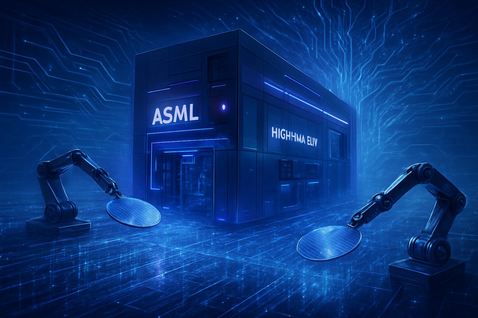
    Engineering the Path to $1 Trillion

    Reaching the trillion-dollar milestone has required a fundamental reimagining of transistor architecture. For over a decade, the industry relied on FinFET (Fin Field-Effect Transistor) technology, but as of early 2026, the "yield war" has officially moved to the Angstrom era. Major manufacturers have transitioned to Gate-All-Around (GAA) or "Nanosheet" transistors, which allow for better electrical control and lower power leakage at sub-2nm scales. Intel (NASDAQ: INTC) has successfully entered high-volume production with its 18A (1.8nm) node, while Taiwan Semiconductor Manufacturing Company (NYSE: TSM) is achieving commercial yields of 60-70% on its N2 (2nm) process.

    The technical specifications of these new chips are staggering. By utilizing High-NA (Numerical Aperture) Extreme Ultraviolet (EUV) lithography, companies are now printing features that are smaller than a single strand of DNA. However, the most significant shift is not just in the chips themselves, but in how they are assembled. Advanced packaging technologies, such as TSMC’s CoWoS (Chip-on-Wafer-on-Substrate) and Intel’s EMIB (Embedded Multi-die Interconnect Bridge), have become the industry's new bottleneck. These "chiplet" designs allow multiple specialized processors to be fused into a single package, providing the massive memory bandwidth required for next-generation AI models.

    Industry experts and researchers have noted that this transition marks the end of "traditional" Moore's Law and the beginning of "System-level Moore's Law." Instead of simply shrinking transistors, the focus has shifted to vertical stacking and backside power delivery—a technique that moves power wiring to the bottom of the wafer to free up space for signals on top. This architectural leap is what enables the massive performance gains seen in the latest AI accelerators, which are now capable of trillions of operations per second while maintaining energy efficiency that was previously thought impossible.

    Corporate Titans and the AI Gold Rush

    The race to $1 trillion has reshaped the corporate hierarchy of the technology world. NVIDIA (NASDAQ: NVDA) has emerged as the undisputed king of this era, recently crossing a $5 trillion market valuation. By evolving from a chip designer into a "full-stack datacenter systems" provider, NVIDIA has secured unprecedented pricing power. Its Blackwell and Rubin platforms, which integrate compute, networking, and software, command prices upwards of $40,000 per unit. For major cloud providers and sovereign nations, securing a steady supply of NVIDIA hardware has become a top strategic priority, often dictating the pace of their own AI deployments.

    While NVIDIA designs the brains, TSMC remains the "Sovereign Foundry" of the world, manufacturing over 90% of the world’s most advanced semiconductors. To mitigate geopolitical risks and meet surging demand, TSMC has adopted a "dual-engine" manufacturing model, accelerating production in its new facilities in Arizona alongside its primary hubs in Taiwan. Meanwhile, Intel is executing one of the most significant turnarounds in industrial history. By reclaiming the technical lead with its 18A node and securing the first fleet of High-NA EUV machines, Intel Foundry has positioned itself as the primary Western alternative to TSMC, attracting a growing list of customers seeking supply chain resilience.

    In the memory sector, Samsung (OTC: SSNLF) and SK Hynix have seen their fortunes soar due to the critical role of High-Bandwidth Memory (HBM). Every advanced AI wafer produced requires an accompanying stack of HBM to function. This has turned memory—once a volatile commodity—into a high-margin, specialized component. As the industry moves toward 2030, the competitive advantage is shifting toward companies that can offer "turnkey" solutions, combining logic, memory, and advanced packaging into a single, optimized ecosystem.

    Geopolitics and the "Intelligence Economy"

    The broader significance of the $1 trillion semiconductor goal lies in its intersection with global politics. Semiconductors are no longer just components; they are instruments of national power. The U.S. CHIPS Act and the EU Chips Act have funneled hundreds of billions of dollars into regionalizing the supply chain, leading to the construction of over 70 new mega-fabs globally. This "technological sovereignty" movement aims to reduce reliance on any single geographic region, particularly as tensions in the Taiwan Strait remain a focal point of global economic concern.

    However, this regionalization comes with significant challenges. As of early 2026, the U.S. has implemented a strict annual licensing framework for high-end chip exports, prompting retaliatory measures from China, including "mineral whitelists" for critical materials like gallium and germanium. This fragmentation of the supply chain has ended the era of "cheap silicon," as the costs of building and operating fabs in multiple regions are passed down to consumers. Despite these costs, the consensus among global leaders is that the price of silicon independence is a necessary investment for national security.

    The shift toward an "Intelligence Economy" also raises concerns about a deepening digital divide. As AI chips become the primary driver of economic productivity, nations and companies with the capital to invest in massive compute clusters will likely pull ahead of those without. This has led to the rise of "Sovereign AI" initiatives, where countries like Japan, Saudi Arabia, and France are investing billions to build their own domestic AI infrastructure, ensuring they are not entirely dependent on American or Chinese technology stacks.

    The Road to 2030: Challenges and the Rise of Physical AI

    Looking toward the end of the decade, the industry is already preparing for the next wave of growth: Physical AI. While the current boom is driven by large language models and software-based agents, the 2027-2030 period is expected to be dominated by robotics and humanoid systems. These applications require even more specialized silicon, including low-latency edge processors and sophisticated sensor fusion chips. Experts predict that the "robotics silicon" market could eventually rival the size of the current smartphone chip market, providing the final push needed to exceed the $1.3 trillion revenue mark by 2030.

    However, several hurdles remain. The industry is facing a "ticking time bomb" in the form of a global talent shortage. By 2030, the gap for skilled semiconductor engineers and technicians is expected to exceed one million workers. Furthermore, the environmental impact of massive new fabs and energy-hungry data centers is coming under increased scrutiny. The next few years will see a massive push for "Green Silicon," focusing on new materials like Silicon Carbide (SiC) and Gallium Nitride (GaN) to improve energy efficiency across the power grid and in electric vehicles.

    The roadmap for the next four years includes the transition to 1.4nm (A14) and eventually 1nm (10A) nodes. These milestones will require even more exotic manufacturing techniques, such as "Directed Self-Assembly" (DSA) and advanced 3D-IC architectures. If the industry can successfully navigate these technical hurdles while managing the volatile geopolitical landscape, the semiconductor sector is poised to become the most valuable industry on the planet, surpassing traditional sectors like oil and gas in terms of strategic and economic importance.

    A New Era of Silicon Dominance

    The journey to a $1 trillion semiconductor industry is a testament to human ingenuity and the relentless pace of technological progress. From the development of GAA transistors to the multi-billion dollar investments in global fabs, the industry has successfully reinvented itself to meet the demands of the AI era. The key takeaway for 2026 is that the semiconductor market is no longer just a bellwether for the tech sector; it is the engine of the entire global economy.

    As we look ahead, the significance of this development in AI history cannot be overstated. We are witnessing the physical construction of the infrastructure that will power the next century of human evolution. The long-term impact will be felt in every sector, from healthcare and education to transportation and defense. Silicon has become the most precious resource of the 21st century, and the companies that control its production will hold the keys to the future.

    In the coming weeks and months, investors and policymakers should watch for updates on the 18A and N2 production yields, as well as any further developments in the "mineral wars" between the U.S. and China. Additionally, the progress of the first wave of "Physical AI" chips will provide a crucial indicator of whether the industry can maintain its current trajectory toward the $1 trillion goal and beyond.


    This content is intended for informational purposes only and represents analysis of current AI developments.

    TokenRing AI delivers enterprise-grade solutions for multi-agent AI workflow orchestration, AI-powered development tools, and seamless remote collaboration platforms.
    For more information, visit https://www.tokenring.ai/.

  • The Packaging Revolution: How Glass Substrates and 3D Stacking Shattered the AI Hardware Bottleneck

    The Packaging Revolution: How Glass Substrates and 3D Stacking Shattered the AI Hardware Bottleneck

    The semiconductor industry has officially entered the "packaging-first" era. As of January 2026, the era of relying solely on shrinking transistors to boost AI performance has ended, replaced by a sophisticated paradigm of 3D integration and advanced materials. The chronic manufacturing bottlenecks that plagued the industry between 2023 and 2025—most notably the shortage of Chip-on-Wafer-on-Substrate (CoWoS) capacity—have been decisively overcome, clearing the path for a new generation of AI processors capable of handling 100-trillion parameter models with unprecedented efficiency.

    This breakthrough is driven by a trifecta of innovations: the commercialization of glass substrates, the maturation of hybrid bonding for 3D IC stacking, and the rapid adoption of the UCIe 3.0 interconnect standard. These technologies have allowed companies to bypass the physical "reticle limit" of a single silicon chip, effectively stitching together dozens of specialized chiplets into a single, massive System-in-Package (SiP). The result is a dramatic leap in bandwidth and power efficiency that is already redefining the competitive landscape for generative AI and high-performance computing.

    Breakthrough Technologies: Glass Substrates and Hybrid Bonding

    The technical cornerstone of this shift is the transition from organic to glass substrates. Leading the charge, Intel (Nasdaq: INTC) has successfully moved glass substrates from pilot programs into high-volume production for its latest AI accelerators. Unlike traditional materials, glass offers a 10-fold increase in routing density and superior thermal stability, which is critical for the massive power draws of modern AI workloads. This allows for ultra-large SiPs that can house over 50 individual chiplets, a feat previously impossible due to material warping and signal degradation.

    Simultaneously, "Hybrid Bonding" has become the gold standard for interconnecting these components. TSMC (NYSE: TSM) has expanded its System-on-Integrated-Chips (SoIC) capacity by 20-fold since 2024, enabling the direct copper-to-copper bonding of logic and memory tiles. This eliminates traditional microbumps, reducing the pitch to as small as 9 micrometers. This advancement is the secret sauce behind NVIDIA’s (Nasdaq: NVDA) new "Rubin" architecture and AMD’s (Nasdaq: AMD) Instinct MI455X, both of which utilize 3D stacking to place HBM4 memory directly atop compute logic.

    Furthermore, the integration of HBM4 (High Bandwidth Memory 4) has effectively shattered the "memory wall." These new modules, featured in the latest silicon from NVIDIA and AMD, offer up to 22 TB/s of bandwidth—double that of the previous generation. By utilizing hybrid bonding to stack up to 16 layers of DRAM, manufacturers are packing nearly 300GB of high-speed memory into a single package, allowing even the largest large language models (LLMs) to reside entirely in-memory during inference.

    Market Impact: Easing Supply and Enabling Custom Silicon

    The resolution of the packaging bottleneck has profound implications for the world’s most valuable tech giants. NVIDIA (Nasdaq: NVDA) remains the primary beneficiary, as the expansion of TSMC’s AP7 and AP8 facilities has finally brought CoWoS supply in line with the insatiable demand for H100, Blackwell, and now Rubin GPUs. With monthly capacity projected to hit 130,000 wafers by the end of 2026, the "supply-constrained" narrative that dominated 2024 has vanished, allowing NVIDIA to accelerate its roadmap to an annual release cycle.

    However, the playing field is also leveling. The ratification of the UCIe 3.0 standard has enabled a "mix-and-match" ecosystem where hyperscalers like Amazon (Nasdaq: AMZN) and Alphabet (Nasdaq: GOOGL) can design custom AI accelerator chiplets and pair them with industry-standard compute tiles from Intel or Samsung (KRX: 005930). This modularity reduces the barrier to entry for custom silicon, potentially disrupting the dominance of off-the-shelf GPUs in specialized cloud environments.

    For equipment manufacturers like ASML (Nasdaq: ASML) and Applied Materials (Nasdaq: AMAT), the packaging boom is a windfall. ASML’s new specialized i-line scanners and Applied Materials' breakthroughs in through-glass via (TGV) etching have become as essential to the supply chain as extreme ultraviolet (EUV) lithography was to the 5nm era. These companies are now the gatekeepers of the "More than Moore" movement, providing the tools necessary to manage the extreme thermal and electrical demands of 2,000-watt AI processors.

    Broader Significance: Extending Moore's Law Through Architecture

    In the broader AI landscape, these breakthroughs represent the successful extension of Moore’s Law through architecture rather than just lithography. By focusing on how chips are connected rather than just how small they are, the industry has avoided a catastrophic stagnation in hardware progress. This is arguably the most significant milestone since the introduction of the first GPU-accelerated neural networks, as it provides the raw compute density required for the next leap in AI: autonomous agents and real-world robotics.

    Yet, this progress brings new challenges, specifically regarding the "Thermal Wall." With AI processors now exceeding 1,000W to 2,000W of total dissipated power (TDP), air cooling has become obsolete for high-end data centers. The industry has been forced to standardize liquid cooling and explore microfluidic channels etched directly into the silicon interposers. This shift is driving a massive infrastructure overhaul in data centers worldwide, raising concerns about the environmental footprint and energy consumption of the burgeoning AI economy.

    Comparatively, the packaging revolution of 2025-2026 mirrors the transition from single-core to multi-core processors in the mid-2000s. Just as multi-core designs saved the PC industry from a thermal dead-end, 3D IC stacking and chiplets have saved AI from a physical size limit. The ability to create "virtual monolithic chips" that are nearly 10 times the size of a standard reticle limit marks a definitive shift in how we conceive of computational power.

    The Future Frontier: Optical Interconnects and Wafer-Scale Systems

    Looking ahead, the near-term focus will be the refinement of "CoPoS" (Chip-on-Panel-on-Substrate). This technique, currently in pilot production at TSMC, moves beyond circular wafers to large rectangular panels, significantly reducing material waste and allowing for even larger interposers. Experts predict that by 2027, we will see the first "wafer-scale" AI systems that are fully integrated using these panel-level packaging techniques, potentially offering a 100x increase in local memory access.

    The long-term frontier lies in optical interconnects. While UCIe 3.0 has maximized the potential of electrical signaling between chiplets, the next bottleneck will be the energy cost of moving data over copper. Research into co-packaged optics (CPO) is accelerating, with the goal of replacing electrical wires with light-based communication within the package itself. If successful, this would virtually eliminate the energy penalty of data movement, paving the way for AI models with quadrillions of parameters.

    The primary challenge remains the complexity of the supply chain. Advanced packaging requires a level of coordination between foundries, memory makers, and assembly houses that is unprecedented. Any disruption in the supply of specialized resins for glass substrates or precision bonding equipment could create new bottlenecks. However, with the massive capital expenditures currently being deployed by Intel, Samsung, and TSMC, the industry is more resilient than it was two years ago.

    A New Foundation for AI

    The advancements in advanced packaging witnessed at the start of 2026 represent a historic pivot in semiconductor manufacturing. By overcoming the CoWoS bottleneck and successfully commercializing glass substrates and 3D stacking, the industry has ensured that the hardware will not be the limiting factor for the next generation of AI. The integration of HBM4 and the standardization of UCIe have created a flexible, high-performance foundation that benefits both established giants and emerging custom-silicon players.

    As we move further into 2026, the key metrics to watch will be the yield rates of glass substrates and the speed at which data centers can adopt the liquid cooling infrastructure required for these high-density chips. This is no longer just a story about chips; it is a story about the complex, multi-dimensional systems that house them. The packaging revolution has not just extended Moore's Law—it has reinvented it for the age of artificial intelligence.


    This content is intended for informational purposes only and represents analysis of current AI developments.

    TokenRing AI delivers enterprise-grade solutions for multi-agent AI workflow orchestration, AI-powered development tools, and seamless remote collaboration platforms.
    For more information, visit https://www.tokenring.ai/.

  • The Silicon Curtain: How ‘Silicon Sovereignty’ and the 2026 NDAA are Redrawing the Global AI Map

    The Silicon Curtain: How ‘Silicon Sovereignty’ and the 2026 NDAA are Redrawing the Global AI Map

    As of January 6, 2026, the global artificial intelligence landscape has been fundamentally reshaped by a series of aggressive U.S. legislative moves and trade pivots that experts are calling the dawn of "Silicon Sovereignty." The centerpiece of this transformation is the National Defense Authorization Act (NDAA) for Fiscal Year 2026, signed into law on December 18, 2025. This landmark legislation, coupled with the new Guaranteeing Access and Innovation for National AI (GAIN) Act, has effectively ended the era of borderless technology, replacing it with a "Silicon Curtain" that prioritizes domestic compute power and national security over global market efficiency.

    The immediate significance of these developments cannot be overstated. For the first time, the U.S. government has mandated a "right-of-first-refusal" for domestic entities seeking advanced AI hardware, ensuring that American startups and researchers are no longer outbid by international state actors or foreign "hyperscalers." Simultaneously, a controversial new "transactional" trade policy has replaced total bans with a 25% revenue-sharing tax on specific mid-tier chip exports to China, a move that attempts to fund U.S. re-industrialization while keeping global rivals tethered to American software ecosystems.

    Technical Foundations: GAIN AI and the Revenue-Share Model

    The technical specifications of the 2026 NDAA and the GAIN AI Act represent a granular approach to technology control. Central to the GAIN AI Act is the "Priority Access" provision, which requires major chipmakers like NVIDIA (NASDAQ: NVDA) and AMD (NASDAQ: AMD) to satisfy all certified domestic orders before fulfilling international contracts for high-performance chips. This policy is specifically targeted at the newest generation of hardware, including the NVIDIA H200 and the upcoming Rubin architecture. Furthermore, the Bureau of Industry and Security (BIS) has introduced a new threshold for "Frontier Model Weights," requiring an export license for any AI model trained using more than 10^26 operations—effectively treating high-level neural network weights as dual-use munitions.

    In a significant shift regarding hardware "chokepoints," the 2026 regulations have expanded to include High Bandwidth Memory (HBM) and advanced packaging equipment. As mass production of HBM4 begins this quarter, led by SK Hynix (KRX: 000660) and Samsung (KRX: 005930), the U.S. has implemented country-wide controls on the 6th-generation memory required to run large-scale AI clusters. This is paired with new restrictions on Deep Ultraviolet (DUV) lithography tools from ASML (NASDAQ: ASML) and packaging machines used for Chip on Wafer on Substrate (CoWoS) processes. By targeting the "packaging gap," the U.S. aims to prevent adversaries from using older "chiplet" architectures to bypass performance caps.

    The most debated technical provision is the "25% Revenue Share" model. Under this rule, the U.S. Treasury allows the export of mid-tier AI chips (such as the H200) to Chinese markets provided the manufacturer pays a 25% surcharge on the gross revenue of the sale. This "digital statecraft" is intended to generate billions for the domestic "Secure Enclave" program, which funds the production of defense-critical silicon in "trusted" facilities, primarily those operated by Intel (NASDAQ: INTC) and TSMC (NYSE: TSM) in Arizona. Initial reactions from the AI research community are mixed; while domestic researchers celebrate the guaranteed hardware access, many warn that the 25% tax may inadvertently accelerate the adoption of domestic Chinese alternatives like Huawei’s Ascend 950PR series.

    Corporate Impact: Navigating the Bifurcated Market

    The impact on tech giants and the broader corporate ecosystem is profound. NVIDIA, which has long dominated the global AI market, now finds itself in a "bifurcated market" strategy. While the company’s stock initially rallied on the news that the Chinese market would partially reopen via the revenue-sharing model, CEO Jensen Huang has warned that the GAIN AI Act's rigid domestic mandates could undermine the predictability of global supply chains. Conversely, domestic-focused AI labs like Anthropic have expressed support for the bill, viewing it as a necessary safeguard for "national survival" in the race toward Artificial General Intelligence (AGI).

    For major "hyperscalers" like Microsoft (NASDAQ: MSFT) and Meta (NASDAQ: META), the new regulations create a complex strategic environment. These companies, which have historically hoarded massive quantities of H100 and B200 chips, must now compete with a federally mandated "waitlist" that prioritizes smaller U.S. startups and defense contractors. This disruption to existing procurement strategies is forcing a shift in market positioning, with many tech giants now lobbying for an expansion of the CHIPS Act to include massive tax credits for domestic power infrastructure and data center construction.

    Startups in the U.S. stand to benefit the most from the GAIN AI Act. By securing a guaranteed supply of cutting-edge silicon, the "compute-poor" tier of the AI ecosystem is finally seeing a leveling of the playing field. However, venture capital firms like Andreessen Horowitz have expressed concerns regarding "outbound investment" controls. The 2026 NDAA restricts U.S. funds from investing in foreign AI firms that utilize restricted hardware, a move that some analysts fear will limit "global intelligence" and visibility into the progress of international competitors.

    Geopolitical Significance: The End of Globalized AI

    The wider significance of "Silicon Sovereignty" marks a definitive end to the era of globalized tech supply chains. This shift is best exemplified by "Pax Silica," an economic security pact signed in late 2025 between the U.S., Japan, South Korea, Taiwan, and the Netherlands. This "Silicon Shield" coordinates export controls and supply chain resilience, creating a unified front against technological proliferation. It represents a transition from a purely commercial landscape to one where silicon is treated with the same strategic weight as oil or nuclear material.

    However, this "Silicon Curtain" brings significant potential concerns. The 25% surcharge on American chips in China makes U.S. technology significantly more expensive, handing a massive price advantage to indigenous Chinese manufacturers. Critics argue that this policy could be a "godsend" for firms like Huawei, accelerating their push for self-sufficiency and potentially crowning them as the dominant hardware providers for the "Global South." This mirrors previous milestones in the Cold War, where technological decoupling often led to the rapid, if inefficient, development of parallel systems.

    Moreover, the focus on "Model Weights" as a restricted commodity introduces a new paradigm for open-source AI. By setting a training threshold of 10^26 operations for export licenses, the U.S. is effectively drawing a line between "safe" consumer AI and "restricted" frontier models. This has sparked a heated debate within the AI community about the future of open-source innovation and whether these restrictions will stifle the very collaborative spirit that fueled the AI boom of 2023-2024.

    Future Horizons: The Packaging War and 2nm Supremacy

    Looking ahead, the next 12 to 24 months will be defined by the "Packaging War" and the 2nm ramp-up. While TSMC’s Arizona facilities are now operational at the 4nm and 3nm nodes, the "technological crown jewel"—the 2nm process—remains centered in Taiwan. U.S. policymakers are expected to increase pressure on TSMC to move more of its advanced packaging (CoWoS) capabilities to American soil to close the "packaging gap" by 2027. Experts predict that the next iteration of the NDAA will likely include provisions for "Sovereign AI Clouds," federally funded data centers designed to provide massive compute power exclusively to "trusted" domestic entities.

    Near-term challenges include the integration of HBM4 and the management of the 25% revenue-share tax. If the tax leads to a total collapse of U.S. chip sales in China due to price sensitivity, the "digital statecraft" model may be abandoned in favor of even stricter bans. Furthermore, as NVIDIA prepares to launch its Rubin architecture in late 2026, the industry will watch closely to see if these chips are even eligible for the revenue-sharing model or if they will be locked behind the "Silicon Curtain" indefinitely.

    Conclusion: A New Era of Digital Statecraft

    In summary, the 2026 NDAA and the GAIN AI Act have codified a new world order for artificial intelligence. The key takeaways are clear: the U.S. has moved from a policy of "containment" to one of "sovereignty," prioritizing domestic access to compute, securing the hardware supply chain through "Pax Silica," and utilizing transactional trade to fund its own re-industrialization. This development is perhaps the most significant in AI history since the release of GPT-4, as it shifts the focus from software capabilities to the raw industrial power required to sustain them.

    The long-term impact of these policies will depend on whether the U.S. can successfully close the "packaging gap" and maintain its lead in lithography. In the coming weeks and months, the industry should watch for the first "revenue-share" licenses to be issued and for the impact of the GAIN AI Act on the Q1 2026 earnings of major semiconductor firms. The "Production Era" of AI has arrived, and the map of the digital world is being redrawn in real-time.


    This content is intended for informational purposes only and represents analysis of current AI developments.

    TokenRing AI delivers enterprise-grade solutions for multi-agent AI workflow orchestration, AI-powered development tools, and seamless remote collaboration platforms.
    For more information, visit https://www.tokenring.ai/.

  • TSMC’s Strategic High-NA Pivot: Balancing Cost and Cutting-Edge Lithography in the AI Era

    TSMC’s Strategic High-NA Pivot: Balancing Cost and Cutting-Edge Lithography in the AI Era

    As of January 2026, the global semiconductor landscape has reached a critical inflection point in the race toward the "Angstrom Era." While the industry watches the rapid evolution of artificial intelligence, Taiwan Semiconductor Manufacturing Company (TSM:NYSE) has officially entered its High-NA EUV (Extreme Ultraviolet) era, albeit with a strategy defined by characteristic caution and economic pragmatism. While competitors like Intel (INTC:NASDAQ) have aggressively integrated ASML (ASML:NASDAQ) latest high-numerical aperture machines into their production lines, TSMC is pursuing a "calculated delay," focusing on refining the technology in its R&D labs while milking the efficiency of its existing fleet for the upcoming A16 and A14 process nodes.

    This strategic divergence marks one of the most significant moments in foundry history. TSMC’s decision to prioritize cost-effectiveness and yield stability over being "first to market" with High-NA hardware is a high-stakes gamble. With AI giants demanding ever-smaller, more power-efficient transistors to fuel the next generation of Large Language Models (LLMs) and autonomous systems, the world’s leading foundry is betting that its mastery of current-generation lithography and advanced packaging will maintain its dominance until the 1.4nm and 1nm nodes become the new industry standard.

    Technical Foundations: The Power of 0.55 NA

    The core of this transition is the ASML Twinscan EXE:5200, a marvel of engineering that represents the most significant leap in lithography in over a decade. Unlike the previous generation of Low-NA (0.33 NA) EUV machines, the High-NA system utilizes a 0.55 numerical aperture to collect more light, enabling a resolution of approximately 8nm. This allows for the printing of features nearly 1.7 times smaller than what was previously possible. For TSMC, the shift to High-NA isn't just about smaller transistors; it’s about reducing the complexity of multi-patterning—a process where a single layer is printed multiple times to achieve fine resolution—which has become increasingly prone to errors at the 2nm scale.

    However, the move to High-NA introduces a significant technical hurdle: the "half-field" challenge. Because of the anamorphic optics required to achieve 0.55 NA, the exposure field of the EXE:5200 is exactly half the size of standard scanners. For massive AI chips like those produced by Nvidia (NVDA:NASDAQ), this requires "field stitching," a process where two halves of a die are printed separately and joined with sub-nanometer precision. TSMC is currently utilizing its R&D units to perfect this stitching and refine the photoresist chemistry, ensuring that when High-NA is finally deployed for high-volume manufacturing (HVM) in the late 2020s, the yield rates will meet the stringent demands of its top-tier customers.

    Competitive Implications and the AI Hardware Boom

    The impact of TSMC’s High-NA strategy ripples across the entire AI ecosystem. Nvidia, currently the world’s most valuable chip designer, stands as both a beneficiary and a strategic balancer in this transition. Nvidia’s upcoming "Rubin" and "Rubin Ultra" architectures, slated for late 2026 and 2027, are expected to leverage TSMC’s 2nm and 1.6nm (A16) nodes. Because these chips are physically massive, Nvidia is leaning heavily into chiplet-based designs and CoWoS-L (Chip on Wafer on Substrate) packaging to bypass the field-size limits of High-NA lithography. By sticking with TSMC’s mature Low-NA processes for now, Nvidia avoids the "bleeding edge" yield risks associated with Intel’s more aggressive High-NA roadmap.

    Meanwhile, Apple (AAPL:NASDAQ) continues to be the primary driver for TSMC’s mobile-first innovations. For the upcoming A19 and A20 chips, Apple is prioritizing transistor density and battery life over the raw resolution gains of High-NA. Industry experts suggest that Apple will likely be the lead customer for TSMC’s A14P node in 2028, which is projected to be the first point of entry for High-NA EUV in consumer electronics. This cautious approach provides a strategic opening for Intel, which has finalized its 14A node using High-NA. In a notable shift, Nvidia even finalized a multi-billion dollar investment in Intel Foundry Services in late 2025 as a hedge, ensuring they have access to High-NA capacity if TSMC’s timeline slips.

    The Broader Significance: Moore’s Law on Life Support

    The transition to High-NA EUV is more than just a hardware upgrade; it is the "life support" for Moore’s Law in an age where AI compute demand is doubling every few months. In the broader AI landscape, the ability to pack nearly three times more transistors into the same silicon area is the only path toward the 100-trillion parameter models envisioned for the end of the decade. However, the sheer cost of this progress is staggering. With each High-NA machine costing upwards of $380 million, the barrier to entry for semiconductor manufacturing has never been higher, further consolidating power among a handful of global players.

    There are also growing concerns regarding power density. As transistors shrink toward the 1nm (A10) mark, managing the thermal output of a 1000W+ AI "superchip" becomes as much a challenge as printing the chip itself. TSMC is addressing this through the implementation of Backside Power Delivery (Super PowerRail) in its A16 node, which moves power routing to the back of the wafer to reduce interference and heat. This synergy between lithography and power delivery is the new frontier of semiconductor physics, echoing the industry's shift from simple scaling to holistic system-level optimization.

    Looking Ahead: The Roadmap to 1nm

    The near-term future for TSMC is focused on the mass production of the A16 node in the second half of 2026. This node will serve as the bridge to the true Angstrom era, utilizing advanced Low-NA techniques to deliver performance gains without the astronomical costs of a full High-NA fleet. Looking further out, the industry expects the A14P node (circa 2028) and the A10 node (2030) to be the true "High-NA workhorses." These nodes will likely be the first to fully adopt 0.55 NA across all critical layers, enabling the next generation of sub-1nm architectures that will power the AI agents and robotics of the 2030s.

    The primary challenge remaining is the economic viability of these sub-1nm processes. Experts predict that as the cost per transistor begins to level off or even rise due to the expense of High-NA, the industry will see an even greater reliance on "More than Moore" strategies. This includes 3D-stacked dies and heterogeneous integration, where only the most critical parts of a chip are made on the expensive High-NA nodes, while less sensitive components are relegated to older, cheaper processes.

    A New Chapter in Silicon History

    TSMC’s entry into the High-NA era, characterized by its "calculated delay," represents a masterclass in industrial strategy. By allowing Intel to bear the initial "pioneer's tax" of debugging ASML’s most complex machines, TSMC is positioning itself to enter the market with higher yields and lower costs when the technology is truly ready for prime time. This development reinforces TSMC's role as the indispensable foundation of the AI revolution, providing the silicon bedrock upon which the future of intelligence is built.

    In the coming weeks and months, the industry will be watching for the first production results from TSMC’s A16 pilot lines and any further shifts in Nvidia’s foundry allocations. As we move deeper into 2026, the success of TSMC’s balanced approach will determine whether it remains the undisputed king of the foundry world or if the aggressive technological leaps of its competitors can finally close the gap. One thing is certain: the High-NA era has arrived, and the chips it produces will define the limits of human and artificial intelligence for decades to come.


    This content is intended for informational purposes only and represents analysis of current AI developments.

    TokenRing AI delivers enterprise-grade solutions for multi-agent AI workflow orchestration, AI-powered development tools, and seamless remote collaboration platforms.
    For more information, visit https://www.tokenring.ai/.

  • Silicon Sovereignty: 2026 Marks the Dawn of the American Semiconductor Renaissance

    Silicon Sovereignty: 2026 Marks the Dawn of the American Semiconductor Renaissance

    The year 2026 has arrived as a definitive watershed moment for the global technology landscape, marking the transition of "Silicon Sovereignty" from a policy ambition to a physical reality. As of January 5, 2026, the United States has successfully re-shored a critical mass of advanced logic manufacturing, effectively ending a decades-long reliance on concentrated Asian supply chains. This shift is headlined by the commencement of high-volume manufacturing at Intel's state-of-the-art facilities in Arizona and the stabilization of TSMC’s domestic operations, signaling a new era where the world's most advanced AI hardware is once again "Made in America."

    The immediate significance of these developments cannot be overstated. For the first time in the modern era, the U.S. domestic supply chain is capable of producing sub-5nm chips at scale, providing a vital "Silicon Shield" against geopolitical volatility in the Taiwan Strait. While the road has been marred by strategic delays in the Midwest and shifting federal priorities, the operational status of the Southwest's "Silicon Desert" hubs confirms that the $52 billion bet placed by the CHIPS and Science Act is finally yielding its high-tech dividends.

    The Arizona Vanguard: 1.8nm and 4nm Realities

    The centerpiece of this manufacturing resurgence is Intel (NASDAQ: INTC) and its Fab 52 at the Ocotillo campus in Chandler, Arizona. As of early 2026, Fab 52 has officially transitioned into High-Volume Manufacturing (HVM) using the company’s ambitious 18A (1.8nm-class) process node. This technical achievement marks the first time a U.S.-based facility has surpassed the 2nm threshold, successfully integrating revolutionary RibbonFET gate-all-around transistors and PowerVia backside power delivery. Intel’s 18A node is currently powering the next generation of Panther Lake AI PC processors and Clearwater Forest server CPUs, with the fab ramping toward a target capacity of 40,000 wafer starts per month.

    Simultaneously, TSMC (NYSE: TSM) has silenced skeptics with the performance of its first Arizona facility, Fab 21. Initially plagued by labor disputes and cultural friction, the fab reached a staggering 92% yield rate for its 4nm (N4) process by the end of 2025—surpassing the yields of its comparable "mother fabs" in Taiwan. This operational efficiency has allowed TSMC to fulfill massive domestic orders for Apple (NASDAQ: AAPL) and Nvidia (NASDAQ: NVDA), ensuring that the silicon driving the world’s most advanced AI models and consumer devices is forged on American soil.

    However, the "Silicon Heartland" narrative has faced a reality check in the Midwest. Intel’s massive "Ohio One" complex in New Albany has seen its production timeline pushed back significantly. Originally slated for a 2025 opening, the facility is now expected to reach high-volume production no earlier than 2030. Intel has characterized this as a "strategic slowing" to align capital expenditures with a softening data center market and to navigate the transition to the "One Big Beautiful Bill Act" (OBBBA) of 2025, which restructured federal semiconductor incentives. Despite the delay, the Ohio site remains a cornerstone of the long-term U.S. strategy, currently serving as a massive shell project that represents a $28 billion commitment to future-proofing the domestic industry.

    Market Dynamics and the New Competitive Moat

    The successful ramp-up of domestic fabs has fundamentally altered the strategic positioning of the world’s largest tech giants. Companies like Nvidia and Apple, which previously faced "single-source" risks tied to Taiwan’s geopolitical status, now possess a diversified manufacturing base. This domestic capacity acts as a competitive moat, insulating these firms from potential export disruptions and the "Silicon Curtain" that has increasingly bifurcated the global market into Western and Eastern technological blocs.

    For Intel, the 2026 milestone is a make-or-break moment for its foundry services. By delivering 18A on schedule in Arizona, Intel is positioning itself as a viable alternative to TSMC for external customers seeking "sovereign-grade" silicon. Meanwhile, Samsung (KRX: 005930) is preparing to join the fray; its Taylor, Texas facility has pivoted exclusively to 2nm Gate-All-Around (GAA) technology. With mass production in Texas expected by late 2026, Samsung is already securing "anchor" AI clients like Tesla (NASDAQ: TSLA), further intensifying the competition for domestic manufacturing dominance.

    This re-shoring effort has also disrupted the traditional cost structures of the industry. Under the new policy frameworks of 2025 and 2026, "trusted" domestic silicon commands a market premium. The introduction of calibrated tariffs—including a 100% duty on Chinese-made semiconductors—has effectively neutralized the price advantage of overseas manufacturing for the U.S. market. This has forced startups and established AI labs alike to prioritize supply chain resilience over pure margin, leading to a surge in long-term domestic supply agreements.

    Geopolitics and the Silicon Shield

    The broader significance of the 2026 landscape lies in the concept of "Silicon Sovereignty." The U.S. government has moved away from the globalized efficiency models of the early 2000s, treating high-end semiconductors as a controlled strategic asset similar to enriched uranium. This "managed restriction" era is designed to ensure that the U.S. maintains a two-generation lead over adversarial nations. The Arizona and Texas hubs now provide a critical buffer; even in a worst-case scenario involving regional instability in Asia, the U.S. is on track to produce 20% of the world's leading-edge logic chips domestically by the end of the decade.

    This shift has also birthed massive public-private partnerships like "Project Stargate," a $500 billion initiative involving Oracle (NYSE: ORCL) and other major players to build hyper-scale AI data centers directly adjacent to these new power and manufacturing hubs. The first Stargate campus in Abilene, Texas, exemplifies the new American industrial model: a vertically integrated ecosystem where energy, silicon, and intelligence are co-located to minimize latency and maximize security.

    However, concerns remain regarding the "Silicon Curtain" and its impact on global innovation. The bifurcation of the market has led to redundant R&D costs and a fragmented standards environment. Critics argue that while the U.S. has secured its own supply, the resulting trade barriers could slow the overall pace of AI development by limiting the cross-pollination of hardware and software breakthroughs between East and West.

    The Horizon: 2nm and Beyond

    Looking toward the late 2020s, the focus is already shifting from 1.8nm to the sub-1nm frontier. The success of the Arizona fabs has set the stage for the next phase of the CHIPS Act, which will likely focus on advanced packaging and "glass substrate" technologies—the next bottleneck in AI chip performance. Experts predict that by 2028, the U.S. will not only lead in chip design but also in the complex assembly and testing processes that are currently concentrated in Southeast Asia.

    The next major challenge will be the workforce. While the facilities are now operational, the industry faces a projected shortfall of 50,000 specialized engineers by 2030. Addressing this "talent gap" through expanded immigration pathways for high-tech workers and domestic vocational programs will be the primary focus of the 2027 policy cycle. If the U.S. can solve the labor equation as successfully as it has the infrastructure equation, the "Silicon Heartland" may eventually span from the deserts of Arizona to the plains of Ohio.

    A New Chapter in Industrial History

    As we reflect on the state of the industry in early 2026, the progress is undeniable. The high-volume output at Intel’s Fab 52 and the high yields at TSMC’s Arizona facility represent a historic reversal of the offshoring trends that defined the last forty years. While the delays in Ohio serve as a reminder of the immense difficulty of building these "most complex machines on Earth," the momentum is clearly on the side of domestic manufacturing.

    The significance of this development in AI history is profound. We have moved from the era of "Software is eating the world" to "Silicon is the world." The ability to manufacture the physical substrate of intelligence domestically is the ultimate form of national security in the 21st century. In the coming months, industry watchers should look for the first 18A-based consumer products to hit the shelves and for Samsung’s Taylor facility to begin its final equipment move-in, signaling the completion of the first great wave of the American semiconductor renaissance.


    This content is intended for informational purposes only and represents analysis of current AI developments.

    TokenRing AI delivers enterprise-grade solutions for multi-agent AI workflow orchestration, AI-powered development tools, and seamless remote collaboration platforms.
    For more information, visit https://www.tokenring.ai/.

  • The Trillion-Dollar Era: The Silicon Super-Cycle Propels Semiconductors to Sovereign Infrastructure Status

    The Trillion-Dollar Era: The Silicon Super-Cycle Propels Semiconductors to Sovereign Infrastructure Status

    As of January 2026, the global semiconductor industry is standing on the precipice of a historic milestone: the $1 trillion annual revenue mark. What was once a notoriously cyclical market defined by the boom-and-bust of consumer electronics has transformed into a structural powerhouse. Driven by the relentless demand for generative AI, the emergence of agentic AI systems, and the total electrification of the automotive sector, the industry has entered a "Silicon Super-Cycle" that shows no signs of slowing down.

    This transition marks a fundamental shift in how the world views compute. Semiconductors are no longer just components in gadgets; they have become the "sovereign infrastructure" of the modern age, as essential to national security and economic stability as energy or transport. With the Americas and the Asia-Pacific regions leading the charge, the industry is projected to hit nearly $976 billion in 2026, with several major investment firms predicting that a surge in high-value AI silicon will push the final tally past the $1 trillion threshold before the year’s end.

    The Technical Engine: Logic, Memory, and the 2nm Frontier

    The backbone of this $1 trillion trajectory is the explosive growth in the Logic and Memory segments, both of which are seeing year-over-year increases exceeding 30%. In the Logic category, the transition to 2-nanometer (2nm) Nanosheet Gate-All-Around (GAA) transistors—spearheaded by Taiwan Semiconductor Manufacturing Company (NYSE: TSM) and Intel Corporation (NASDAQ: INTC) via its 18A node—has provided the necessary performance-per-watt jump to sustain massive AI clusters. These advanced nodes allow for a 30% reduction in power consumption, a critical factor as data center energy demands become a primary bottleneck for scaling intelligence.

    In the Memory sector, the "Memory Supercycle" is being fueled by the mass adoption of High Bandwidth Memory 4 (HBM4). As AI models transition from simple generation to complex reasoning, the need for rapid data access has made HBM4 a strategic asset. Manufacturers like SK Hynix (KRX: 000660) and Micron Technology (NASDAQ: MU) are reporting record-breaking margins as HBM4 becomes the standard for million-GPU clusters. This high-performance memory is no longer a niche requirement but a fundamental component of the "Agentic AI" architecture, which requires massive, low-latency memory pools to facilitate autonomous decision-making.

    The technical specifications of 2026-era hardware are staggering. NVIDIA (NASDAQ: NVDA) and its Rubin architecture have reset the pricing floor for the industry, with individual AI accelerators commanding prices between $30,000 and $40,000. These units are not just processors; they are integrated systems-on-chip (SoCs) that combine logic, high-speed networking, and stacked memory into a single package. The industry has moved away from general-purpose silicon toward these highly specialized, high-margin AI platforms, driving the dramatic increase in Average Selling Prices (ASP) that is catapulting revenue toward the trillion-dollar mark.

    Initial reactions from the research community suggest that we are entering a "Validation Phase" of AI. While the previous two years were defined by training Large Language Models (LLMs), 2026 is the year of scaled inference and agentic execution. Experts note that the hardware being deployed today is specifically optimized for "chain-of-thought" processing, allowing AI agents to perform multi-step tasks autonomously. This shift from "chatbots" to "agents" has necessitated a complete redesign of the silicon stack, favoring custom ASICs (Application-Specific Integrated Circuits) designed by hyperscalers like Alphabet (NASDAQ: GOOGL) and Amazon (NASDAQ: AMZN).

    Market Dynamics: From Cyclical Goods to Global Utility

    The move toward $1 trillion has fundamentally altered the competitive landscape for tech giants and startups alike. For companies like NVIDIA and Advanced Micro Devices (NASDAQ: AMD), the challenge has shifted from finding customers to managing a supply chain that is now considered a matter of national interest. The "Silicon Super-Cycle" has reduced the historical volatility of the sector; because compute is now viewed as an infinite, non-discretionary resource for the enterprise, the traditional "bust" phase of the cycle has been replaced by a steady, high-growth plateau.

    Major cloud providers, including Microsoft (NASDAQ: MSFT) and Meta (NASDAQ: META), are no longer just customers of the semiconductor industry—they are becoming integral parts of its design ecosystem. By developing their own custom silicon to run specific AI workloads, these hyperscalers are creating a "structural alpha" in their operations, reducing their reliance on third-party vendors while simultaneously driving up the total market value of the semiconductor space. This vertical integration has forced legacy chipmakers to innovate faster, leading to a competitive environment where the "winner-takes-most" in the high-end AI segment.

    Regional dominance is also shifting, with the Americas emerging as a high-value design and demand hub. Projected to grow by over 34% in 2026, the U.S. market is benefiting from the concentration of AI hyperscalers and the ramping up of domestic fabrication facilities in Arizona and Ohio. Meanwhile, the Asia-Pacific region, led by the manufacturing prowess of Taiwan and South Korea, remains the largest overall market by revenue. This regionalization of the supply chain, fueled by government subsidies and the pursuit of "Sovereign AI," has created a more robust, albeit more expensive, global infrastructure.

    For startups, the $1 trillion era presents both opportunities and barriers. While the high cost of advanced-node silicon makes it difficult for new entrants to compete in general-purpose AI hardware, a new wave of "Edge AI" startups is thriving. These companies are focusing on specialized chips for robotics and software-defined vehicles (SDVs), where the power and cost requirements are different from those of massive data centers. By carving out these niches, startups are ensuring that the semiconductor ecosystem remains diverse even as the giants consolidate their hold on the core AI infrastructure.

    The Geopolitical and Societal Shift to Sovereign AI

    The broader significance of the semiconductor industry reaching $1 trillion cannot be overstated. We are witnessing the birth of "Sovereign AI," where nations view their compute capacity as a direct reflection of their geopolitical power. Governments are no longer content to rely on a globalized supply chain; instead, they are investing billions to ensure that they have domestic access to the chips that power their economies, defense systems, and public services. This has turned the semiconductor industry into a cornerstone of national policy, comparable to the role of oil in the 20th century.

    This shift to "essential infrastructure" brings with it significant concerns regarding equity and access. As the price of high-end silicon continues to climb, a "compute divide" is emerging between those who can afford to build and run massive AI models and those who cannot. The concentration of power in a handful of companies and regions—specifically the U.S. and East Asia—has led to calls for more international cooperation to ensure that the benefits of the AI revolution are distributed more broadly. However, in the current climate of "silicon nationalism," such cooperation remains elusive.

    Comparisons to previous milestones, such as the rise of the internet or the mobile revolution, often fall short of describing the current scale of change. While the internet connected the world, the $1 trillion semiconductor industry is providing the "brains" for every physical and digital system on the planet. From autonomous fleets of electric vehicles to agentic AI systems that manage global logistics, the silicon being manufactured today is the foundation for a new type of cognitive economy. This is not just a technological breakthrough; it is a structural reset of the global industrial order.

    Furthermore, the environmental impact of this growth is a growing point of contention. The massive energy requirements of AI data centers and the water-intensive nature of advanced semiconductor fabrication are forcing the industry to lead in green technology. The push for 2nm and 1.4nm nodes is driven as much by the need for energy efficiency as it is by the need for speed. As the industry approaches the $1 trillion mark, its ability to decouple growth from environmental degradation will be the ultimate test of its sustainability as a global utility.

    Future Horizons: Agentic AI and the Road to 1.4nm

    Looking ahead, the next two to three years will be defined by the maturation of Agentic AI. Unlike generative AI, which requires human prompts, agentic systems will operate autonomously within the enterprise, handling everything from software development to supply chain management. This will require a new generation of "inference-first" silicon that can handle continuous, low-latency reasoning. Experts predict that by 2027, the demand for inference hardware will officially surpass the demand for training hardware, leading to a second wave of growth for the Logic segment.

    In the automotive sector, the transition to Software-Defined Vehicles (SDVs) is expected to accelerate. As Level 3 and Level 4 autonomous features become standard in new electric vehicles, the semiconductor content per car is projected to double again by 2028. This will create a massive, stable demand for power semiconductors and high-performance automotive compute, providing a hedge against any potential cooling in the data center market. The integration of AI into the physical world—through robotics and autonomous transport—is the next frontier for the $1 trillion industry.

    Technical challenges remain, particularly as the industry approaches the physical limits of silicon. The move toward 1.4nm nodes and the adoption of "High-NA" EUV (Extreme Ultraviolet) lithography from ASML (NASDAQ: ASML) will be the next major hurdles. These technologies are incredibly complex and expensive, and any delays could temporarily slow the industry's momentum. However, with the world's largest economies now treating silicon as a strategic necessity, the level of investment and talent being poured into these challenges is unprecedented in human history.

    Conclusion: A Milestone in the History of Technology

    The trajectory toward a $1 trillion semiconductor industry by 2026 is more than just a financial milestone; it is a testament to the central role that compute now plays in our lives. From the "Silicon Super-Cycle" driven by AI to the regional shifts in manufacturing and design, the industry has successfully transitioned from a cyclical commodity market to the essential infrastructure of the 21st century. The dominance of Logic and Memory, fueled by breakthroughs in 2nm nodes and HBM4, has created a foundation for the next decade of innovation.

    As we look toward the coming months, the industry's ability to navigate geopolitical tensions and environmental challenges will be critical. The "Sovereign AI" movement is likely to accelerate, leading to more regionalized supply chains and a continued focus on domestic fabrication. For investors, policymakers, and consumers, the message is clear: the semiconductor industry is no longer a sector of the economy—it is the economy. The $1 trillion mark is just the beginning of a new era where silicon is the most valuable resource on Earth.


    This content is intended for informational purposes only and represents analysis of current AI developments.

    TokenRing AI delivers enterprise-grade solutions for multi-agent AI workflow orchestration, AI-powered development tools, and seamless remote collaboration platforms.
    For more information, visit https://www.tokenring.ai/.

  • The Nanosheet Era Begins: TSMC Commences 2nm Mass Production, Powering the Next Decade of AI

    The Nanosheet Era Begins: TSMC Commences 2nm Mass Production, Powering the Next Decade of AI

    As of January 5, 2026, the global semiconductor landscape has officially shifted. Taiwan Semiconductor Manufacturing Company (NYSE: TSM) has announced the successful commencement of mass production for its 2nm (N2) process technology, marking the industry’s first large-scale transition to Nanosheet Gate-All-Around (GAA) transistors. This milestone, centered at the company’s state-of-the-art Fab 20 and Fab 22 facilities, represents the most significant architectural change in chip manufacturing in over a decade, promising to break the efficiency bottlenecks that have begun to plague the artificial intelligence and mobile computing sectors.

    The immediate significance of this development cannot be overstated. With 2nm capacity already reported as overbooked through the end of the year, the move to N2 is not merely a technical upgrade but a strategic linchpin for the world’s most valuable technology firms. By delivering a 15% increase in speed and a staggering 30% reduction in power consumption compared to the previous 3nm node, TSMC is providing the essential hardware foundation required to sustain the current "AI supercycle" and the next generation of energy-conscious consumer electronics.

    A Fundamental Shift: Nanosheet GAA and the Rise of Fab 20 & 22

    The transition to the N2 node marks TSMC’s formal departure from the FinFET (Fin Field-Effect Transistor) architecture, which has been the industry standard since the 16nm era. The new Nanosheet GAA technology utilizes horizontal stacks of silicon "sheets" entirely surrounded by the transistor gate on all four sides. This design provides superior electrostatic control, drastically reducing the current leakage that had become a growing concern as transistors approached atomic scales. By allowing chip designers to adjust the width of these nanosheets, TSMC has introduced a level of "width scalability" that enables a more precise balance between high-performance computing and low-power efficiency.

    Production is currently anchored in two primary hubs in Taiwan. Fab 20, located in the Hsinchu Science Park, served as the initial bridge from research to pilot production and is now operating at scale. Simultaneously, Fab 22 in Kaohsiung—a massive "Gigafab" complex—has activated its first phase of 2nm production to meet the massive volume requirements of global clients. Initial reports suggest that TSMC has achieved yield rates between 60% and 70%, an impressive feat for a first-generation GAA process, which has historically been difficult for competitors like Samsung (KRX: 005930) and Intel (NASDAQ: INTC) to stabilize at high volumes.

    Industry experts have reacted with a mix of awe and relief. "The move to GAA was the industry's biggest hurdle in continuing Moore's Law," noted one lead analyst at a top semiconductor research firm. "TSMC's ability to hit volume production in early 2026 with stable yields effectively secures the roadmap for AI model scaling and mobile performance for the next three years. This isn't just an iteration; it’s a new foundation for silicon physics."

    The Silicon Elite: Capacity War and Market Positioning

    The arrival of 2nm silicon has triggered an unprecedented scramble among tech giants, resulting in an overbooked order book that spans well into 2027. Apple (NASDAQ: AAPL) has once again secured its position as the primary anchor customer, reportedly claiming over 50% of the initial 2nm capacity. These chips are destined for the upcoming A20 processors in the iPhone 18 series and the M6 series of MacBooks, giving Apple a significant lead in power efficiency and on-device AI processing capabilities compared to its rivals.

    NVIDIA (NASDAQ: NVDA) and AMD (NASDAQ: AMD) are also at the forefront of this transition, driven by the insatiable power demands of data centers. NVIDIA is transitioning its high-end compute tiles for the "Rubin" GPU architecture to 2nm to combat the "power wall" that threatens the expansion of massive AI training clusters. Similarly, AMD has confirmed that its Zen 6 "Venice" CPUs and MI450 AI accelerators will leverage the N2 node. This early adoption allows these companies to maintain a competitive edge in the high-performance computing (HPC) market, where every percentage point of energy efficiency translates into millions of dollars in saved operational costs for cloud providers.

    For competitors like Intel, the pressure is mounting. While Intel has its own 18A node (equivalent to the 1.8nm class) entering the market, TSMC’s successful 2nm ramp-up reinforces its dominance as the world’s most reliable foundry. The strategic advantage for TSMC lies not just in the technology, but in its ability to manufacture these complex chips at a scale that no other firm can currently match. With 2nm wafers reportedly priced at a premium of $30,000 each, the barrier to entry for the "Silicon Elite" has never been higher, further consolidating power among the industry's wealthiest players.

    AI and the Energy Imperative: Wider Implications

    The shift to 2nm is occurring at a critical juncture for the broader AI landscape. As large language models (LLMs) grow in complexity, the energy required to train and run them has become a primary bottleneck for the industry. The 30% power reduction offered by the N2 node is not just a technical specification; it is a vital necessity for the sustainability of AI expansion. By reducing the thermal footprint of data centers, TSMC is enabling the next wave of AI breakthroughs that would have been physically or economically impossible on 3nm or 5nm hardware.

    This milestone also signals a pivot toward "AI-first" silicon design. Unlike previous nodes where mobile phones were the sole drivers of innovation, the N2 node has been optimized from the ground up for high-performance computing. This reflects a broader trend where the semiconductor industry is no longer just serving consumer electronics but is the literal engine of the global digital economy. The transition to GAA technology ensures that the industry can continue to pack more transistors into a given area, maintaining the momentum of Moore’s Law even as traditional scaling methods hit their physical limits.

    However, the move to 2nm also raises concerns regarding the geographical concentration of advanced chipmaking. With Fab 20 and Fab 22 both located in Taiwan, the global tech economy remains heavily dependent on a single region for its most critical hardware. While TSMC is expanding its footprint in Arizona, those facilities are not expected to reach 2nm parity until 2027 or later. This creates a "silicon shield" that is as much a geopolitical factor as it is a technological one, keeping the global spotlight firmly on the stability of the Taiwan Strait.

    The Angstrom Roadmap: N2P, A16, and Super Power Rail

    Looking beyond the current N2 milestone, TSMC has already laid out an aggressive roadmap for the "Angstrom Era." By the second half of 2026, the company expects to introduce N2P, a performance-enhanced version of the 2nm node that will likely be adopted by flagship Android SoC makers like Qualcomm (NASDAQ: QCOM) and MediaTek (TWSE: 2454). N2P is expected to offer incremental gains in performance and power, refining the GAA process as it matures.

    The most anticipated leap, however, is the A16 (1.6nm) node, slated for mass production in late 2026. The A16 node will introduce "Super Power Rail" technology, TSMC’s proprietary version of Backside Power Delivery (BSPDN). This revolutionary approach moves the entire power distribution network to the backside of the wafer, connecting it directly to the transistor's source and drain. By separating the power and signal paths, Super Power Rail eliminates voltage drops and frees up significant space on the front side of the chip for signal routing.

    Experts predict that the combination of GAA and Super Power Rail will define the next five years of semiconductor innovation. The A16 node is projected to offer an additional 10% speed increase and a 20% power reduction over N2P. As AI models move toward real-time multi-modal processing and autonomous agents, these technical leaps will be essential for providing the necessary "compute-per-watt" to make such applications viable on mobile devices and edge hardware.

    A Landmark in Computing History

    TSMC’s successful mass production of 2nm chips in January 2026 will be remembered as the moment the semiconductor industry successfully navigated the transition from FinFET to Nanosheet GAA. This shift is more than a routine node shrink; it is a fundamental re-engineering of the transistor that ensures the continued growth of artificial intelligence and high-performance computing. With the roadmap for N2P and A16 already in motion, the "Angstrom Era" is no longer a theoretical future but a tangible reality.

    The key takeaway for the coming months will be the speed at which TSMC can scale its yield and how quickly its primary customers—Apple, NVIDIA, and AMD—can bring their 2nm-powered products to market. As the first 2nm-powered devices begin to appear later this year, the gap between the "Silicon Elite" and the rest of the industry is likely to widen, driven by the immense performance and efficiency gains of the N2 node.

    In the long term, this development solidifies TSMC’s position as the indispensable architect of the modern world. While challenges remain—including geopolitical tensions and the rising costs of wafer production—the commencement of 2nm mass production proves that the limits of silicon are still being pushed further than many thought possible. The AI revolution has found its new engine, and it is built on a foundation of nanosheets.


    This content is intended for informational purposes only and represents analysis of current AI developments.

    TokenRing AI delivers enterprise-grade solutions for multi-agent AI workflow orchestration, AI-powered development tools, and seamless remote collaboration platforms.
    For more information, visit https://www.tokenring.ai/.

  • OpenAI’s Silicon Sovereignty: The Multi-Billion Dollar Shift to In-House AI Chips

    OpenAI’s Silicon Sovereignty: The Multi-Billion Dollar Shift to In-House AI Chips

    In a move that marks the end of the "GPU-only" era for the world’s leading artificial intelligence lab, OpenAI has officially transitioned into a vertically integrated hardware powerhouse. As of early 2026, the company has solidified its custom silicon strategy, moving beyond its role as a software developer to become a major player in semiconductor design. By forging deep strategic alliances with Broadcom (NASDAQ:AVGO) and TSMC (NYSE:TSM), OpenAI is now deploying its first generation of in-house AI inference chips, a move designed to shatter its near-total dependency on NVIDIA (NASDAQ:NVDA) and fundamentally rewrite the economics of large-scale AI.

    This shift represents a massive gamble on "Silicon Sovereignty"—the idea that to achieve Artificial General Intelligence (AGI), a company must control the entire stack, from the foundational code to the very transistors that execute it. The immediate significance of this development cannot be overstated: by bypassing the "NVIDIA tax" and designing chips tailored specifically for its proprietary Transformer architectures, OpenAI aims to reduce its compute costs by as much as 50%. This cost reduction is essential for the commercial viability of its increasingly complex "reasoning" models, which require significantly more compute per query than previous generations.

    The Architecture of "Project Titan": Inside OpenAI’s First ASIC

    At the heart of OpenAI’s hardware push is a custom Application-Specific Integrated Circuit (ASIC) often referred to internally as "Project Titan." Unlike the general-purpose H100 or Blackwell GPUs from NVIDIA, which are designed to handle a wide variety of tasks from gaming to scientific simulation, OpenAI’s chip is a specialized "XPU" optimized almost exclusively for inference—the process of running a pre-trained model to generate responses. Led by Richard Ho, the former lead of the Google (NASDAQ:GOOGL) TPU program, the engineering team has utilized a systolic array design. This architecture allows data to flow through a grid of processing elements in a highly efficient pipeline, minimizing the energy-intensive data movement that plagues traditional chip designs.

    Technical specifications for the 2026 rollout are formidable. The first generation of chips, manufactured on TSMC’s 3nm (N3) process, incorporates High Bandwidth Memory (HBM3E) to handle the massive parameter counts of the GPT-5 and o1-series models. However, OpenAI has already secured capacity for TSMC’s upcoming A16 (1.6nm) node, which is expected to integrate HBM4 and deliver a 20% increase in power efficiency. Furthermore, OpenAI has opted for an "Ethernet-first" networking strategy, utilizing Broadcom’s Tomahawk switches and optical interconnects. This allows OpenAI to scale its custom silicon across massive clusters without the proprietary lock-in of NVIDIA’s InfiniBand or NVLink technologies.

    The development process itself was a landmark for AI-assisted engineering. OpenAI reportedly used its own "reasoning" models to optimize the physical layout of the chip, achieving area reductions and thermal efficiencies that human engineers alone might have taken months to perfect. This "AI-designing-AI" feedback loop has allowed OpenAI to move from initial concept to a "taped-out" design in record time, surprising many industry veterans who expected the company to spend years in the R&D phase.

    Reshaping the Semiconductor Power Dynamics

    The market implications of OpenAI’s silicon strategy have sent shockwaves through the tech sector. While NVIDIA remains the undisputed king of AI training, OpenAI’s move to in-house inference chips has begun to erode NVIDIA’s dominance in the high-margin inference market. Analysts estimate that by late 2025, inference accounted for over 60% of total AI compute spending, and OpenAI’s transition could represent billions in lost revenue for NVIDIA over the coming years. Despite this, NVIDIA continues to thrive on the back of its Blackwell and upcoming Rubin architectures, though its once-impenetrable "CUDA moat" is showing signs of stress as OpenAI shifts its software to the hardware-agnostic Triton framework.

    The clear winners in this new paradigm are Broadcom and TSMC. Broadcom has effectively become the "foundry for the fabless," providing the essential intellectual property and design platforms that allow companies like OpenAI and Meta (NASDAQ:META) to build custom silicon without owning a single factory. For TSMC, the partnership reinforces its position as the indispensable foundation of the global economy; with its 3nm and 2nm nodes fully booked through 2027, the Taiwanese giant has implemented price hikes that reflect its immense leverage over the AI industry.

    This move also places OpenAI in direct competition with the "hyperscalers"—Google, Amazon (NASDAQ:AMZN), and Microsoft (NASDAQ:MSFT)—all of whom have their own custom silicon programs (TPU, Trainium, and Maia, respectively). However, OpenAI’s strategy differs in its exclusivity. While Amazon and Google rent their chips to third parties via the cloud, OpenAI’s silicon is a "closed-loop" system. It is designed specifically to make running the world’s most advanced AI models economically viable for OpenAI itself, providing a competitive edge in the "Token Economics War" where the company with the lowest marginal cost of intelligence wins.

    The "Silicon Sovereignty" Trend and the End of the Monopoly

    OpenAI’s foray into hardware fits into a broader global trend of "Silicon Sovereignty." In an era where AI compute is viewed as a strategic resource on par with oil or electricity, relying on a single vendor for hardware is increasingly seen as a catastrophic business risk. By designing its own chips, OpenAI is insulating itself from supply chain shocks, geopolitical tensions, and the pricing whims of a monopoly provider. This is a significant milestone in AI history, echoing the moment when early tech giants like IBM (NYSE:IBM) or Apple (NASDAQ:AAPL) realized that to truly innovate in software, they had to master the hardware beneath it.

    However, this transition is not without its concerns. The sheer scale of OpenAI’s ambitions—exemplified by the rumored $500 billion "Stargate" supercomputer project—has raised questions about energy consumption and environmental impact. OpenAI’s roadmap targets a staggering 10 GW to 33 GW of compute capacity by 2029, a figure that would require the equivalent of multiple nuclear power plants to sustain. Critics argue that the race for silicon sovereignty is accelerating an unsustainable energy arms race, even if the custom chips themselves are more efficient than the general-purpose GPUs they replace.

    Furthermore, the "Great Decoupling" from NVIDIA’s CUDA platform marks a shift toward a more fragmented software ecosystem. While OpenAI’s Triton language makes it easier to run models on various hardware, the industry is moving away from a unified standard. This could lead to a world where AI development is siloed within the hardware ecosystems of a few dominant players, potentially stifling the open-source community and smaller startups that cannot afford to design their own silicon.

    The Road to Stargate and Beyond

    Looking ahead, the next 24 months will be critical as OpenAI scales its "Project Titan" chips from initial pilot racks to full-scale data center deployment. The long-term goal is the integration of these chips into "Stargate," the massive AI supercomputer being developed in partnership with Microsoft. If successful, Stargate will be the largest concentrated collection of compute power in human history, providing the "compute-dense" environment necessary for the next leap in AI: models that can reason, plan, and verify their own outputs in real-time.

    Future iterations of OpenAI’s silicon are expected to lean even more heavily into "low-precision" computing. Experts predict that by 2027, OpenAI will be using FP4 or even INT8 precision for its most advanced reasoning tasks, allowing for even higher throughput and lower power consumption. The challenge remains the integration of these chips with emerging memory technologies like HBM4, which will be necessary to keep up with the exponential growth in model parameters.

    Experts also predict that OpenAI may eventually expand its silicon strategy to include "edge" devices. While the current focus is on massive data centers, the ability to run high-quality inference on local hardware—such as AI-integrated laptops or specialized robotics—could be the next frontier. As OpenAI continues to hire aggressively from the silicon teams of Apple, Google, and Intel (NASDAQ:INTC), the boundary between an AI research lab and a semiconductor powerhouse will continue to blur.

    A New Chapter in the AI Era

    OpenAI’s transition to custom silicon is a definitive moment in the evolution of the technology industry. It signals that the era of "AI as a Service" is maturing into an era of "AI as Infrastructure." By taking control of its hardware destiny, OpenAI is not just trying to save money; it is building the foundation for a future where high-level intelligence is a ubiquitous and inexpensive utility. The partnership with Broadcom and TSMC has provided the technical scaffolding for this transition, but the ultimate success will depend on OpenAI's ability to execute at a scale that few companies have ever attempted.

    The key takeaways are clear: the "NVIDIA monopoly" is being challenged not by another chipmaker, but by NVIDIA’s own largest customers. The "Silicon Sovereignty" movement is now the dominant strategy for the world’s most powerful AI labs, and the "Great Decoupling" from proprietary hardware stacks is well underway. As we move deeper into 2026, the industry will be watching closely to see if OpenAI’s custom silicon can deliver on its promise of 50% lower costs and 100% independence.

    In the coming months, the focus will shift to the first performance benchmarks of "Project Titan" in production environments. If these chips can match or exceed the performance of NVIDIA’s Blackwell in real-world inference tasks, it will mark the beginning of a new chapter in AI history—one where the intelligence of the model is inseparable from the silicon it was born to run on.


    This content is intended for informational purposes only and represents analysis of current AI developments.

    TokenRing AI delivers enterprise-grade solutions for multi-agent AI workflow orchestration, AI-powered development tools, and seamless remote collaboration platforms.
    For more information, visit https://www.tokenring.ai/.

  • The $1 Trillion Horizon: Semiconductors Enter the Era of the Silicon Super-Cycle

    The $1 Trillion Horizon: Semiconductors Enter the Era of the Silicon Super-Cycle

    As of January 2, 2026, the global semiconductor industry has officially entered what analysts are calling the "Silicon Super-Cycle." Following a record-breaking 2025 that saw industry revenues soar past $800 billion, new data suggests the sector is now on an irreversible trajectory to exceed $1 trillion in annual revenue by 2030. This monumental growth is no longer speculative; it is being cemented by the relentless expansion of generative AI infrastructure, the total electrification of the automotive sector, and a new generation of "Agentic" IoT devices that require unprecedented levels of on-device intelligence.

    The significance of this milestone cannot be overstated. For decades, the semiconductor market was defined by cyclical booms and busts tied to PC and smartphone demand. However, the current era represents a structural shift where silicon has become the foundational commodity of the global economy—as essential as oil was in the 20th century. With the industry growing at a compound annual growth rate (CAGR) of over 8%, the race to $1 trillion is being led by a handful of titans who are redefining the limits of physics and manufacturing.

    The Technical Engine: 2nm, 18A, and the Rubin Revolution

    The technical landscape of 2026 is dominated by a fundamental shift in transistor architecture. For the first time in over a decade, the industry has moved away from the FinFET (Fin Field-Effect Transistor) design that powered the previous generation of electronics. Taiwan Semiconductor Manufacturing Company (NYSE: TSM), commonly known as TSMC, has successfully ramped up its 2nm (N2) process, utilizing Nanosheet Gate-All-Around (GAA) transistors. This transition allows for a 15% performance boost or a 30% reduction in power consumption compared to the 3nm nodes of 2024.

    Simultaneously, Intel (NASDAQ: INTC) has achieved a major milestone with its 18A (1.8nm) process, which entered high-volume production at its Arizona facilities this month. The 18A node introduces "PowerVia," the industry’s first implementation of backside power delivery, which separates the power lines from the data lines on a chip to reduce interference and improve efficiency. This technical leap has allowed Intel to secure major foundry customers, including a landmark partnership with NVIDIA (NASDAQ: NVDA) for specialized AI components.

    On the architectural front, NVIDIA has just begun shipping its "Rubin" R100 GPUs, the successor to the Blackwell line. The Rubin architecture is the first to fully integrate the HBM4 (High Bandwidth Memory 4) standard, which doubles the memory bus width to 2048-bit and provides a staggering 2.0 TB/s of peak throughput per stack. This leap in memory performance is critical for "Agentic AI"—autonomous AI systems that require massive local memory to process complex reasoning tasks in real-time without constant cloud polling.

    The Beneficiaries: NVIDIA’s Dominance and the Foundry Wars

    The primary beneficiary of this $1 trillion march remains NVIDIA, which briefly touched a $5 trillion market capitalization in late 2025. By controlling over 90% of the AI accelerator market, NVIDIA has effectively become the gatekeeper of the AI era. However, the competitive landscape is shifting. Advanced Micro Devices (NASDAQ: AMD) has gained significant ground with its MI400 series, capturing nearly 15% of the data center market by offering a more open software ecosystem compared to NVIDIA’s proprietary CUDA platform.

    The "Foundry Wars" have also intensified. While TSMC still holds a dominant 70% market share, the resurgence of Intel Foundry and the steady progress of Samsung (KRX: 005930) have created a more fragmented market. Samsung recently secured a $16.5 billion deal with Tesla (NASDAQ: TSLA) to produce next-generation Full Self-Driving (FSD) chips using its 3nm GAA process. Meanwhile, Broadcom (NASDAQ: AVGO) and Marvell (NASDAQ: MRVL) are seeing record revenues as "hyperscalers" like Google and Amazon shift toward custom-designed AI ASICs (Application-Specific Integrated Circuits) to reduce their reliance on off-the-shelf GPUs.

    This shift toward customization is disrupting the traditional "one-size-fits-all" chip model. Startups specializing in "Edge AI" are finding fertile ground as the market moves from training large models in the cloud to running them on local devices. Companies that can provide high-performance, low-power silicon for the "Intelligence of Things" are increasingly becoming acquisition targets for tech giants looking to vertically integrate their hardware stacks.

    The Global Stakes: Geopolitics and the Environmental Toll

    As the semiconductor industry scales toward $1 trillion, it has become the primary theater of global geopolitical competition. The U.S. CHIPS Act has transitioned from a funding phase to an operational one, with several leading-edge "mega-fabs" now online in the United States. This has created a strategic buffer, yet the world remains heavily dependent on the "Silicon Shield" of Taiwan. In late 2025, simulated blockades in the Taiwan Strait sent shockwaves through the market, highlighting that even a minor disruption in the region could risk a $500 billion hit to the global economy.

    Beyond geopolitics, the environmental impact of a $1 trillion industry is coming under intense scrutiny. A single modern mega-fab in 2026 consumes as much as 10 million gallons of ultrapure water per day and requires energy levels equivalent to a small city. The transition to 2nm and 1.8nm nodes has increased energy intensity by nearly 3.5x compared to legacy nodes. In response, the industry is pivoting toward "Circular Silicon" initiatives, with TSMC and Intel pledging to recycle 85% of their water and transition to 100% renewable energy by 2030 to mitigate regulatory pressure and resource scarcity.

    This environmental friction is a new phenomenon for the industry. Unlike the software booms of the past, the semiconductor super-cycle is tied to physical constraints—land, water, power, and rare earth minerals. The ability of a company to secure "green" manufacturing capacity is becoming as much of a competitive advantage as the transistor density of its chips.

    The Road to 2030: Edge AI and the Intelligence of Things

    Looking ahead, the next four years will be defined by the migration of AI from the data center to the "Edge." While the current revenue surge is driven by massive server farms, the path to $1 trillion will be paved by the billions of devices in our pockets, homes, and cars. We are entering the era of the "Intelligence of Things" (IoT 2.0), where every sensor and appliance will possess enough local compute power to run sophisticated AI agents.

    In the automotive sector, the semiconductor content per vehicle is expected to double by 2030. Modern Electric Vehicles (EVs) are essentially data centers on wheels, requiring high-power silicon carbide (SiC) semiconductors for power management and high-end SoCs (System on a Chip) for autonomous navigation. Qualcomm (NASDAQ: QCOM) is positioning itself as a leader in this space, leveraging its mobile expertise to dominate the "Digital Cockpit" market.

    Experts predict that the next major breakthrough will involve Silicon Photonics—using light instead of electricity to move data between chips. This technology, expected to hit the mainstream by 2028, could solve the "interconnect bottleneck" that currently limits the scale of AI clusters. As we approach the end of the decade, the integration of quantum-classical hybrid chips is also expected to emerge, providing a new frontier for specialized scientific computing.

    A New Industrial Bedrock

    The semiconductor industry's journey to $1 trillion is a testament to the central role of hardware in the AI revolution. The key takeaway from early 2026 is that the industry has successfully navigated the transition to GAA transistors and localized manufacturing, creating a more resilient, albeit more expensive, global supply chain. The "Silicon Super-Cycle" is no longer just about faster computers; it is about the infrastructure of modern life.

    In the history of technology, this period will likely be remembered as the moment semiconductors surpassed the automotive and energy industries in strategic importance. The long-term impact will be a world where intelligence is "baked in" to every physical object, driven by the chips currently rolling off the assembly lines in Hsinchu, Phoenix, and Magdeburg.

    In the coming weeks and months, investors and industry watchers should keep a eye on the yield rates of 2nm production and the first real-world benchmarks of NVIDIA’s Rubin GPUs. These metrics will determine which companies will capture the lion's share of the final $200 billion climb to the trillion-dollar mark.


    This content is intended for informational purposes only and represents analysis of current AI developments.

    TokenRing AI delivers enterprise-grade solutions for multi-agent AI workflow orchestration, AI-powered development tools, and seamless remote collaboration platforms.
    For more information, visit https://www.tokenring.ai/.

  • The CoWoS Crunch Ends: TSMC Unleashes Massive Packaging Expansion to Power the 2026 AI Supercycle

    The CoWoS Crunch Ends: TSMC Unleashes Massive Packaging Expansion to Power the 2026 AI Supercycle

    As of January 2, 2026, the global semiconductor landscape has reached a definitive turning point. After two years of "packaging-bound" constraints that throttled the supply of high-end artificial intelligence processors, Taiwan Semiconductor Manufacturing Company (NYSE:TSM) has officially entered a new era of hyper-scale production. By aggressively expanding its Chip on Wafer on Substrate (CoWoS) capacity, TSMC is finally clearing the bottlenecks that once forced lead times for AI servers to stretch beyond 50 weeks, signaling a massive shift in how the industry builds the engines of the generative AI revolution.

    This expansion is not merely an incremental upgrade; it is a structural transformation of the silicon supply chain. By the end of 2025, TSMC successfully nearly doubled its CoWoS output to 75,000 wafers per month, and current projections for 2026 suggest the company will hit a staggering 130,000 wafers per month by year-end. This surge in capacity is specifically designed to meet the insatiable appetite for NVIDIA’s Blackwell and upcoming Rubin architectures, as well as AMD’s MI350 series, ensuring that the next generation of Large Language Models (LLMs) and autonomous systems are no longer held back by the physical limits of chip assembly.

    The Technical Evolution of Advanced Packaging

    The technical evolution of advanced packaging has become the new frontline of Moore’s Law. While traditional chip scaling—making transistors smaller—has slowed, TSMC’s CoWoS technology allows multiple "chiplets" to be interconnected on a single interposer, effectively creating a "superchip" that behaves like a single, massive processor. The current industry standard has shifted from the mature CoWoS-S (Standard) to the more complex CoWoS-L (Local Silicon Interconnect). CoWoS-L utilizes an RDL interposer with embedded silicon bridges, allowing for modular designs that can exceed the traditional "reticle limit" of a single silicon wafer.

    This shift is critical for the latest hardware. NVIDIA (NASDAQ:NVDA) is utilizing CoWoS-L for its Blackwell (B200) GPUs to connect two high-performance logic dies with eight stacks of High Bandwidth Memory (HBM3e). Looking ahead to the Rubin (R100) architecture, which is entering trial production in early 2026, the requirements become even more extreme. Rubin will adopt a 3nm process and a massive 4x reticle size interposer, integrating up to 12 stacks of next-generation HBM4. Without the capacity expansion at TSMC’s new facilities, such as the massive AP8 plant in Tainan, these chips would be nearly impossible to manufacture at scale.

    Industry experts note that this transition represents a departure from the "monolithic" chip era. By using CoWoS, manufacturers can mix and match different components—such as specialized AI accelerators, I/O dies, and memory—onto a single package. This approach significantly improves yield rates, as it is easier to manufacture several small, perfect dies than one giant, flawless one. The AI research community has lauded this development, as it directly enables the multi-terabyte-per-second memory bandwidth required for the trillion-parameter models currently under development.

    Competitive Implications for the AI Giants

    The primary beneficiary of this capacity surge remains NVIDIA, which has reportedly secured over 60% of TSMC’s total 2026 CoWoS output. This strategic "lock-in" gives NVIDIA a formidable moat, allowing it to maintain its dominant market share by ensuring its customers—ranging from hyperscalers like Microsoft and Google to sovereign AI initiatives—can actually receive the hardware they order. However, the expansion also opens the door for Advanced Micro Devices (NASDAQ:AMD), which is using TSMC’s SoIC (System-on-Integrated-Chip) and CoWoS-S technologies for its MI325 and MI350X accelerators to challenge NVIDIA’s performance lead.

    The competitive landscape is further complicated by the entry of Broadcom (NASDAQ:AVGO) and Marvell Technology (NASDAQ:MRVL), both of which are leveraging TSMC’s advanced packaging to build custom AI ASICs (Application-Specific Integrated Circuits) for major cloud providers. As packaging capacity becomes more available, the "premium" price of AI compute may begin to stabilize, potentially disrupting the high-margin environment that has fueled record profits for chipmakers over the last 24 months.

    Meanwhile, Intel (NASDAQ:INTC) is attempting to position its Foundry Services as a viable alternative, promoting its EMIB (Embedded Multi-die Interconnect Bridge) and Foveros technologies. While Intel has made strides in securing smaller contracts, the high cost of porting designs away from TSMC’s ecosystem has kept the largest AI players loyal to the Taiwanese giant. Samsung (KRX:005930) has also struggled to gain ground; despite offering "turnkey" solutions that combine HBM production with packaging, yield issues on its advanced nodes have allowed TSMC to maintain its lead.

    Broader Significance for the AI Landscape

    The broader significance of this development lies in the realization that the "compute" bottleneck has been replaced by a "connectivity" bottleneck. In the early 2020s, the industry focused on how many transistors could fit on a chip. In 2026, the focus has shifted to how fast those chips can talk to each other and their memory. TSMC’s expansion of CoWoS is the physical manifestation of this shift, marking a transition into the "3D Silicon" era where the vertical and horizontal integration of chips is as important as the lithography used to print them.

    This trend has profound geopolitical implications. The concentration of advanced packaging capacity in Taiwan remains a point of concern for global supply chain resilience. While TSMC is expanding its footprint in Arizona and Japan, the most cutting-edge "CoW" (Chip-on-Wafer) processes remain centered in facilities like the new Chiayi AP7 plant. This ensures that Taiwan remains the indispensable "silicon shield" of the global economy, even as Western nations push for more localized semiconductor manufacturing.

    Furthermore, the environmental impact of these massive packaging facilities is coming under scrutiny. Advanced packaging requires significant amounts of ultrapure water and electricity, leading to localized tensions in regions like Chiayi. As the AI industry continues to scale, the sustainability of these manufacturing hubs will become a central theme in corporate social responsibility reports and government regulations, mirroring the debates currently surrounding the energy consumption of AI data centers.

    Future Developments in Silicon Integration

    Looking toward the near-term future, the next major milestone will be the widespread adoption of glass substrates. While current CoWoS technology relies on silicon or organic interposers, glass offers superior thermal stability and flatter surfaces, which are essential for the ultra-fine interconnects required for HBM4 and beyond. TSMC and its partners are already conducting pilot runs with glass substrates, with full-scale integration expected by late 2027 or 2028.

    Another area of rapid development is the integration of optical interconnects directly into the package. As electrical signals struggle to travel across large substrates without significant power loss, "Silicon Photonics" will allow chips to communicate using light. This will enable the creation of "warehouse-scale" computers where thousands of GPUs function as a single, unified processor. Experts predict that the first commercial AI chips featuring integrated co-packaged optics (CPO) will begin appearing in high-end data centers within the next 18 to 24 months.

    A Comprehensive Wrap-Up

    In summary, TSMC’s aggressive expansion of its CoWoS capacity is the final piece of the puzzle for the current AI boom. By resolving the packaging bottlenecks that defined 2024 and 2025, the company has cleared the way for a massive influx of high-performance hardware. The move cements TSMC’s role as the foundation of the AI era and underscores the reality that advanced packaging is no longer a "back-end" process, but the primary driver of semiconductor innovation.

    As we move through 2026, the industry will be watching closely to see if this surge in supply leads to a cooling of the AI market or if the demand for even larger models will continue to outpace production. For now, the "CoWoS Crunch" is effectively over, and the race to build the next generation of artificial intelligence has entered a high-octane new phase.


    This content is intended for informational purposes only and represents analysis of current AI developments.

    TokenRing AI delivers enterprise-grade solutions for multi-agent AI workflow orchestration, AI-powered development tools, and seamless remote collaboration platforms.
    For more information, visit https://www.tokenring.ai/.