As 2025 draws to a close, the landscape of American semiconductor manufacturing has reached a dramatic inflection point, revealing a stark divergence between the industry’s two most prominent players. Taiwan Semiconductor Manufacturing Company (NYSE: TSM) has defied early skepticism by announcing that its Arizona "Fab 21" has officially reached profitability, successfully transitioning to high-volume manufacturing of 4nm and 5nm nodes with yields that now surpass its domestic facilities in Taiwan. This milestone marks a significant victory for the U.S. government’s efforts to repatriate critical technology production.
In sharp contrast, Intel Corporation (Nasdaq: INTC) has concluded the year by confirming a substantial "strategic slowing of construction" for its massive "Ohio One" project in New Albany. Once hailed as the future "Silicon Heartland," the completion of the first Ohio fab has been officially pushed back to 2030, with high-volume production not expected until 2031. As Intel navigates a complex financial stabilization period, the divergence between these two projects highlights the immense technical and economic challenges of scaling leading-edge logic manufacturing on American soil.
Technical Milestones and Yield Realities
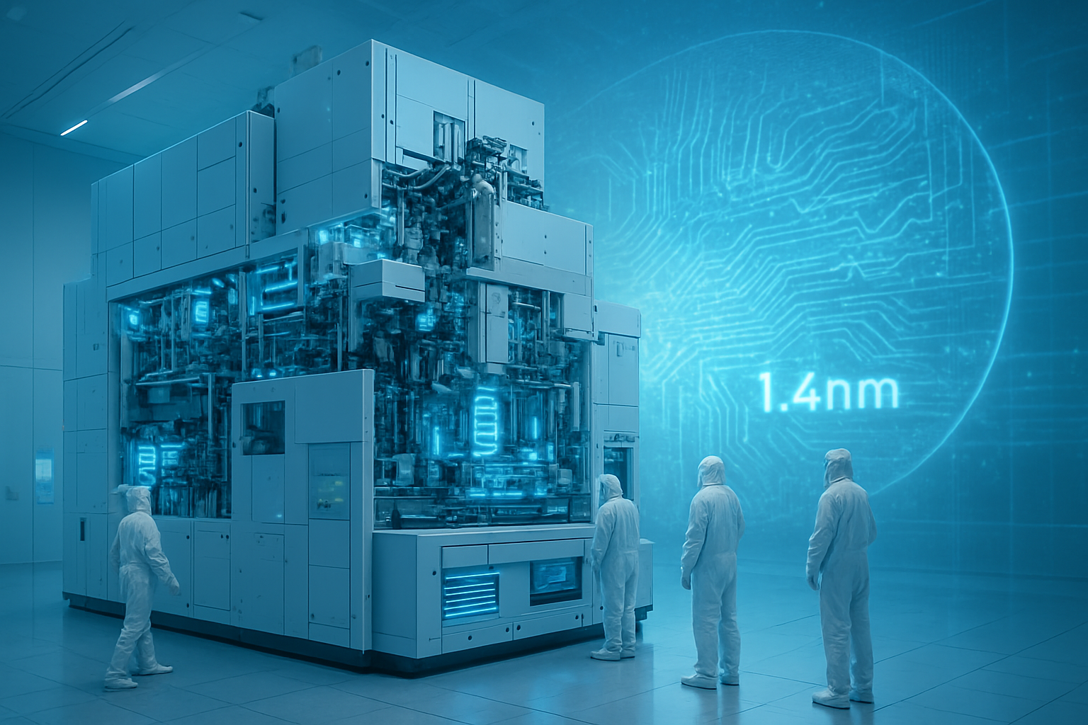
The technical success of TSMC’s Phase 1 facility in North Phoenix has surprised even the most optimistic industry analysts. By December 2025, Fab 21 achieved a landmark yield rate of 92% for its 4nm (N4P) process, a figure that notably exceeds the 88% yield rates typically seen in TSMC’s "mother fabs" in Hsinchu, Taiwan. This achievement is attributed to a rigorous "copy-exactly" strategy and the successful integration of a local workforce that many feared would struggle with the precision required for sub-7nm manufacturing. With Phase 1 fully operational, TSMC has already completed construction on Phase 2, with 3nm equipment installation slated for early 2026.
Intel’s technical journey in 2025 has been more arduous. The company’s turnaround strategy remains pinned to its 18A (1.8nm-class) process node, which reached a "usable" yield range of 65% to 70% this month. While this represents a massive recovery from the 10% risk-production yields reported earlier in the year, it remains below the threshold required for the high-margin profitability Intel needs to fund its ambitious domestic expansion. Consequently, the "Ohio One" site, while physically shelled, has seen its "tool-in" phase delayed. Intel’s first 18A consumer chips, the Panther Lake series, have begun a "slow and deliberate" market entry, serving more as a proof-of-concept for the 18A architecture than a high-volume revenue driver.
Strategic Shifts and Corporate Maneuvering
The financial health of these two giants has dictated their 2025 trajectories. TSMC Arizona recorded its first-ever net profit in the first half of 2025, bolstered by high utilization rates from anchor clients including Apple Inc. (Nasdaq: AAPL), NVIDIA Corporation (Nasdaq: NVDA), and Advanced Micro Devices (Nasdaq: AMD). These tech giants have increasingly prioritized "Made in USA" silicon to satisfy both geopolitical de-risking and domestic content requirements, ensuring that TSMC’s Arizona capacity was pre-sold long before the first wafers were etched.
Intel, meanwhile, has spent 2025 in a "healing phase," focusing on radical financial restructuring. In a move that sent shockwaves through the industry in August, NVIDIA Corporation (Nasdaq: NVDA) made a $5 billion equity investment in Intel to ensure the long-term viability of a domestic foundry alternative. This was followed by the U.S. government taking a unique $8.9 billion equity stake in Intel via the CHIPS and Science Act, effectively making the Department of Commerce a passive stakeholder. These capital infusions, combined with a 20% reduction in Intel's global workforce and the spin-off of its manufacturing unit into an independent entity, have stabilized Intel’s balance sheet but necessitated the multi-year delay of the Ohio project to conserve cash.
The Geopolitical and Economic Landscape
The broader significance of this divergence cannot be overstated. The CHIPS and Science Act has acted as the financial backbone for both firms, but the ROI is manifesting differently. TSMC’s success in Arizona validates the Act’s goal of bringing the world’s most advanced manufacturing to U.S. shores, with the company even breaking ground on a Phase 3 expansion in April 2025 to produce 2nm and 1.6nm (A16) chips. The "Building Chips in America" Act (BCAA), signed in late 2024, further assisted by streamlining environmental reviews, allowing TSMC to accelerate its expansion while Intel used the same legislative breathing room to pause and pivot.
However, the delay of Intel’s Ohio project to 2030 raises concerns about the "Silicon Heartland" narrative. While Intel remains committed to the site—having invested over $3.7 billion by the start of 2025—the local economic impact in New Albany has shifted from an immediate boom to a long-term waiting game. This delay highlights a potential vulnerability in the U.S. strategy: while foreign-owned fabs like TSMC are thriving on American soil, the "national champion" is struggling to maintain the same pace, leading to a domestic ecosystem that is increasingly reliant on Taiwanese IP to meet its immediate high-end chip needs.
Future Outlook and Emerging Challenges
Looking ahead to 2026 and beyond, the industry will be watching TSMC’s Phase 2 ramp-up. If the company can replicate its 4nm success with 3nm and 2nm nodes in Arizona, it will cement the state as the premier global hub for advanced logic. The primary challenge for TSMC will be maintaining these yields as they move toward the A16 Angstrom-era nodes, which involve complex backside power delivery and new transistor architectures that have never been mass-produced outside of Taiwan.
For Intel, the next five years will be a period of "disciplined execution." The goal is to reach 18A maturity in its Oregon and Arizona development sites before attempting the massive scale-up in Ohio. Experts predict that if Intel can successfully stabilize its independent foundry business and attract more third-party customers like NVIDIA or Microsoft, the 2030 opening of the Ohio fab could coincide with the launch of its 14A or 10A nodes, potentially leapfrogging the current competition. The challenge remains whether Intel can sustain investor and government patience over such a long horizon.
A New Era for American Silicon
As we close the book on 2025, the "Tale of Two Fabs" serves as a masterclass in the complexities of modern industrial policy. TSMC has proven that with enough capital and a "copy-exactly" mindset, the world’s most advanced technology can be successfully transplanted across oceans. Its Arizona profitability is a watershed moment in the history of the semiconductor industry, proving that the U.S. can be a competitive location for high-volume, leading-edge manufacturing.
Intel’s delay in Ohio, while disappointing to local stakeholders, represents a necessary strategic retreat to ensure the company’s survival. By prioritizing financial stability and yield refinement over rapid physical expansion, Intel is betting that it is better to be late and successful than early and unprofitable. In the coming months, the industry will closely monitor TSMC’s 3nm tool-in and Intel’s progress in securing more external foundry customers—the two key metrics that will determine who truly wins the race for American silicon supremacy in the decade to come.
This content is intended for informational purposes only and represents analysis of current AI and semiconductor developments.
TokenRing AI delivers enterprise-grade solutions for multi-agent AI workflow orchestration, AI-powered development tools, and seamless remote collaboration platforms.
For more information, visit https://www.tokenring.ai/.