As the world enters the final months of 2025, the global semiconductor landscape is undergoing a seismic shift. Taiwan Semiconductor Manufacturing Company (NYSE: TSM), the world’s largest contract chipmaker, has officially detailed its roadmap for the "Angstrom Era," centering on the highly anticipated A14 (1.4nm) process node. This announcement comes at a pivotal moment as TSMC confirms that its N2 (2nm) node has reached full-scale mass production in Taiwan, marking the industry’s first successful transition to nanosheet transistor architecture at volume.
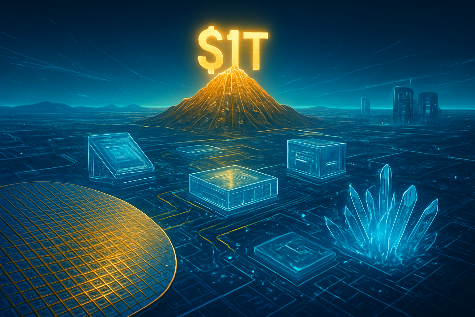
The roadmap is not merely a technical achievement; it is a strategic fortification of TSMC's dominance. By outlining a clear path to 1.4nm production by 2028 and simultaneously accelerating its manufacturing footprint in the United States, TSMC is signaling its intent to remain the indispensable partner for the AI revolution. With the demand for high-performance computing (HPC) and energy-efficient AI silicon reaching unprecedented levels, the move to A14 represents the next frontier in Moore’s Law, promising to pack more than a trillion transistors on a single package by the end of the decade.
Technical Mastery: The A14 Node and the High-NA EUV Gamble
The A14 node, which TSMC expects to enter risk production in late 2027 followed by volume production in 2028, represents a refined evolution of the Gate-All-Around (GAA) nanosheet transistors debuting with the current N2 node. Technically, A14 is projected to deliver a 15% performance boost at the same power level or a 25–30% reduction in power consumption compared to N2. Logic density is also expected to jump by over 20%, a critical metric for the massive GPU clusters required by next-generation LLMs. To achieve this, TSMC is introducing "NanoFlex Pro," a design-technology co-optimization (DTCO) tool that allows chip designers from companies like NVIDIA (NASDAQ: NVDA) and Apple (NASDAQ: AAPL) to mix high-performance and high-density cells within a single block, maximizing efficiency.
Perhaps the most discussed aspect of the A14 roadmap is TSMC’s decision to bypass High-NA EUV (Extreme Ultraviolet) lithography for the initial phase of 1.4nm production. While Intel (NASDAQ: INTC) has aggressively adopted the $380 million machines from ASML (NASDAQ: ASML) for its 14A node, TSMC has opted to stick with its proven 0.33-NA EUV tools combined with advanced multi-patterning. TSMC leadership argued in late 2025 that the economic maturity and yield stability of standard EUV outweigh the resolution benefits of High-NA for the first generation of A14. This "yield-first" strategy aims to avoid the production bottlenecks that have historically plagued aggressive lithography transitions, ensuring that high-volume clients receive predictable delivery schedules.
The Competitive Chessboard: Fending Off Intel and Samsung
The A14 announcement sets the stage for a high-stakes showdown in the late 2020s. Intel’s "IDM 2.0" strategy is currently in its most critical phase, with the company betting that its early adoption of High-NA EUV and "PowerVia" backside power delivery will allow its 14A node to leapfrog TSMC by 2027. Meanwhile, Samsung (KRX: 005930) is aggressively marketing its SF1.4 node, leveraging its longer experience with GAA transistors—which it first introduced at the 3nm stage—to lure AI startups away from the TSMC ecosystem with competitive pricing and earlier access to 1.4nm prototypes.
Despite these challenges, TSMC’s market positioning remains formidable. The company’s "Super Power Rail" (SPR) technology, set to debut on the intermediate A16 (1.6nm) node in 2026, will provide a bridge for customers who need backside power delivery before the full A14 transition. For major players like AMD (NASDAQ: AMD) and Broadcom (NASDAQ: AVGO), the continuity of TSMC’s ecosystem—including its industry-leading CoWoS (Chip-on-Wafer-on-Substrate) advanced packaging—creates a "stickiness" that is difficult for competitors to break. Industry analysts suggest that while Intel may win the race to the first High-NA chip, TSMC’s ability to manufacture millions of 1.4nm chips with high yields will likely preserve its 60%+ market share.
Arizona’s Evolution: From Satellite Fab to Silicon Hub
Parallel to its technical roadmap, TSMC has significantly ramped up its expansion in the United States. As of December 2025, Fab 21 in Phoenix, Arizona, has moved beyond its initial teething issues. Phase 1 (Module 1) is now in full volume production of 4nm and 5nm chips, with internal reports suggesting yield rates that match or even exceed those of TSMC’s Tainan facilities. This success has emboldened the company to accelerate Phase 2, which will now bring 3nm (N3) production to U.S. soil by 2027, a year earlier than originally planned.
The wider significance of this expansion cannot be overstated. With the groundbreaking of Phase 3 in April 2025, TSMC has committed to producing 2nm and eventually A16 (1.6nm) chips in Arizona by 2029. This creates a geographically diversified supply chain that addresses the "single point of failure" concerns regarding Taiwan’s geopolitical situation. For the U.S. government and domestic tech giants, the presence of a leading-edge 1.6nm fab in the desert provides a level of silicon security that was unimaginable at the start of the decade. It also fosters a local ecosystem of suppliers and talent, turning Phoenix into a global center for semiconductor R&D that rivals Hsinchu.
Beyond 1nm: The Future of the Atomic Scale
Looking toward 2030, the challenges of scaling silicon are becoming increasingly physical rather than just economic. As TSMC nears the 1nm threshold, the industry is beginning to look at Complementary FET (CFET) architectures, which stack n-type and p-type transistors on top of each other to further save space. Researchers at TSMC are also exploring 2D materials like molybdenum disulfide (MoS2) to replace silicon channels, which could allow for even thinner transistors with better electrical properties.
The transition to A14 and beyond will also require a revolution in thermal management. As power density increases, the heat generated by these microscopic circuits becomes a major hurdle. Future developments are expected to focus heavily on integrated liquid cooling and new dielectric materials to prevent "thermal runaway" in AI accelerators. Experts predict that while the "nanometer" naming convention is becoming more of a marketing term than a literal measurement, the drive toward atomic-scale precision will continue to push the boundaries of materials science and quantum physics.
Conclusion: TSMC’s Unyielding Momentum
TSMC’s roadmap to A14 and the maturation of its Arizona operations solidify its role as the backbone of the global digital economy. By balancing aggressive scaling with a pragmatic approach to new equipment like High-NA EUV, the company has managed to maintain a "golden ratio" of innovation and reliability. The successful ramp-up of 2nm production in late 2025 serves as a proof of concept for the nanosheet era, providing a stable foundation for the even more ambitious 1.4nm goals.
In the coming months, the industry will be watching closely for the first 2nm chip benchmarks from Apple’s next-generation processors and NVIDIA’s future Blackwell-successors. Furthermore, the continued integration of advanced packaging in Arizona will be a key indicator of whether the U.S. can truly support a full-stack semiconductor ecosystem. As we head into 2026, one thing is certain: the race to 1nm is no longer a sprint, but a marathon of endurance, precision, and immense capital investment, with TSMC still holding the lead.
This content is intended for informational purposes only and represents analysis of current AI developments.
TokenRing AI delivers enterprise-grade solutions for multi-agent AI workflow orchestration, AI-powered development tools, and seamless remote collaboration platforms.
For more information, visit https://www.tokenring.ai/.